TAIPEI, Taiwan – October 16, 2025 – Taiwan Semiconductor Manufacturing Company (TSMC) (NYSE: TSM), the world's preeminent contract chip manufacturer, today announced a significant upward revision of its full-year 2025 revenue forecast. This bullish outlook is directly attributed to the unprecedented and accelerating demand for artificial intelligence (AI) chips, underscoring TSMC's indispensable role as the foundational architect of the burgeoning AI supercycle. The company now anticipates its 2025 revenue to grow by the mid-30% range in U.S. dollar terms, a notable increase from its previous projection of approximately 30%.
The announcement, coinciding with robust third-quarter results that surpassed market expectations, solidifies the notion that AI is not merely a transient trend but a profound, transformative force reshaping the global technology landscape. TSMC's financial performance acts as a crucial barometer for the entire AI ecosystem, with its advanced manufacturing capabilities becoming the bottleneck and enabler for virtually every major AI breakthrough, from generative AI models to autonomous systems and high-performance computing.
The Silicon Engine of AI: Advanced Nodes and Packaging Drive Unprecedented Performance
TSMC's escalating revenue forecast is rooted in its unparalleled technological leadership in both miniaturized process nodes and sophisticated advanced packaging solutions. This shift represents a fundamental reorientation of demand drivers, moving decisively from traditional consumer electronics to the intense, specialized computational needs of AI and high-performance computing (HPC).
The company's advanced process nodes are at the heart of this AI revolution. Its 3nm family (N3, N3E, N3P), which commenced high-volume production in December 2022, now forms the bedrock for many cutting-edge AI chips. In Q3 2025, 3nm chips contributed a substantial 23% of TSMC's total wafer revenue. The 5nm nodes (N5, N5P, N4P), introduced in 2020, also remain critical, accounting for 37% of wafer revenue in the same quarter. Combined, these advanced nodes (7nm and below) generated 74% of TSMC's wafer revenue, demonstrating their dominance in current AI chip manufacturing. These smaller nodes dramatically increase transistor density, boosting computational capabilities, enhancing performance by 10-15% with each generation, and improving power efficiency by 25-35% compared to their predecessors—all critical factors for the demanding requirements of AI workloads.
Beyond mere miniaturization, TSMC's advanced packaging technologies are equally pivotal. Solutions like CoWoS (Chip-on-Wafer-on-Substrate) are indispensable for overcoming the "memory wall" and enabling the extreme parallelism required by AI. CoWoS integrates multiple dies, such as GPUs and High Bandwidth Memory (HBM) stacks, on a silicon interposer, delivering significantly higher bandwidth (up to 8.6 Tb/s) and lower latency. This technology is fundamental to cutting-edge AI GPUs like NVIDIA's H100 and upcoming architectures. Furthermore, TSMC's SoIC (System-on-Integrated-Chips) offers advanced 3D stacking for ultra-high-density vertical integration, promising even greater bandwidth and power integrity for future AI and HPC applications, with mass production planned for 2025. The company is aggressively expanding its CoWoS capacity, aiming to quadruple output by the end of 2025 and increase SoIC capacity eightfold by 2026.
This current surge in demand marks a significant departure from previous eras, where new process nodes were primarily driven by smartphone manufacturers. While mobile remains important, the primary impetus for cutting-edge chip technology has decisively shifted to the insatiable computational needs of AI and HPC for data centers, large language models, and custom AI silicon. Major hyperscalers are increasingly designing their own custom AI chips (ASICs), relying heavily on TSMC for their manufacturing, highlighting that advanced chip hardware is now a critical strategic differentiator.
A Ripple Effect Across the AI Ecosystem: Winners, Challengers, and Strategic Imperatives
TSMC's dominant position in advanced semiconductor manufacturing sends profound ripples across the entire AI industry, significantly influencing the competitive landscape and conferring strategic advantages upon its key partners. With an estimated 70-71% market share in the global pure-play wafer foundry market, and an even higher share in advanced AI chip segments, TSMC is the indispensable enabler for virtually all leading AI hardware.
Fabless semiconductor giants and tech behemoths are the primary beneficiaries. NVIDIA (NASDAQ: NVDA), a cornerstone client, heavily relies on TSMC for manufacturing its cutting-edge GPUs, including the H100 and future architectures, with CoWoS packaging being crucial. Apple (NASDAQ: AAPL) leverages TSMC's 3nm process for its M4 and M5 chips, powering on-device AI, and has reportedly secured significant 2nm capacity. Advanced Micro Devices (NASDAQ: AMD) utilizes TSMC's advanced packaging and leading-edge nodes for its next-generation data center GPUs (MI300 series) and EPYC CPUs, positioning itself as a strong challenger in the HPC market. Hyperscale cloud providers like Alphabet (NASDAQ: GOOGL) (Google), Amazon (NASDAQ: AMZN), Meta Platforms (NASDAQ: META), and Microsoft (NASDAQ: MSFT) are increasingly designing custom AI silicon (ASICs) to optimize performance for their specific workloads, relying almost exclusively on TSMC for manufacturing.
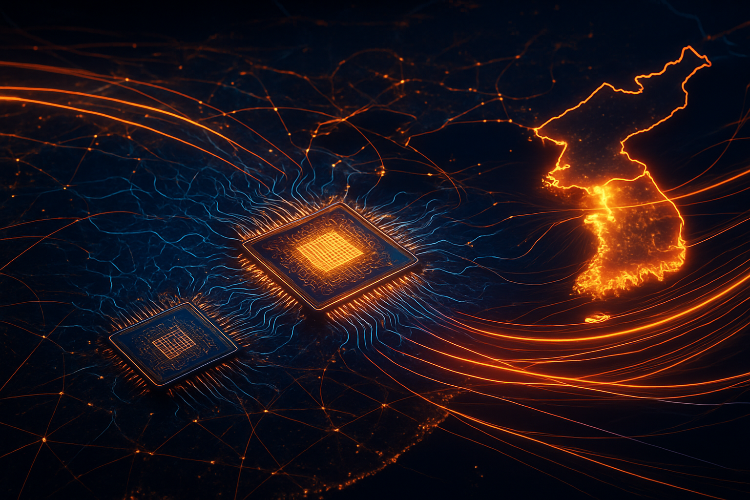
However, this centralization around TSMC also creates competitive implications and potential disruptions. The company's near-monopoly in advanced AI chip manufacturing establishes substantial barriers to entry for newer firms or those lacking significant capital and strategic partnerships. Major tech companies are highly dependent on TSMC's technological roadmap and manufacturing capacity, influencing their product development cycles and market strategies. This dependence, while enabling rapid innovation, also accelerates hardware obsolescence, compelling continuous upgrades to AI infrastructure. Geopolitical risks, particularly the extreme concentration of advanced chip manufacturing in Taiwan, pose significant vulnerabilities. U.S. export controls aimed at curbing China's AI ambitions directly impact Chinese AI chip firms, limiting their access to TSMC's advanced nodes and forcing them to downgrade designs, thus impacting their ability to compete at the leading edge.
For companies that can secure access to TSMC's capabilities, the strategic advantages are immense. Access to cutting-edge process nodes (e.g., 3nm, 2nm) and advanced packaging (e.g., CoWoS) is a strategic imperative, conferring significant market positioning and competitive advantages by enabling the development of the most powerful and energy-efficient AI systems. This access directly accelerates AI innovation, allowing for superior performance and energy efficiency crucial for modern AI models. TSMC also benefits from a "client lock-in ecosystem" due to its yield superiority and the prohibitive switching costs for clients, reinforcing its technological moat.
The Broader Canvas: AI Supercycle, Geopolitics, and a New Industrial Revolution
TSMC's AI-driven revenue forecast is not merely a financial highlight; it's a profound indicator of the broader AI landscape and its transformative trajectory. This performance solidifies the ongoing "AI supercycle," an era characterized by exponential growth in AI capabilities and deployment, comparable in its foundational impact to previous technological shifts like the internet, mobile computing, and cloud computing.
The robust demand for TSMC's advanced chips, particularly from leading AI chip designers, underscores how the AI boom is structurally transforming the semiconductor sector. This demand for high-performance chips is offsetting declines in traditional markets, indicating a fundamental shift where computing power, energy efficiency, and fabrication precision are paramount. The global AI chip market is projected to skyrocket to an astonishing $311.58 billion by 2029, with AI-related spending reaching approximately $1.5 trillion by 2025 and over $2 trillion in 2026. TSMC's position ensures that it is at the nexus of this economic catalyst, driving innovation and investment across the entire tech ecosystem.
However, this pivotal role also brings significant concerns. The extreme supply chain concentration, particularly in the Taiwan Strait, presents considerable geopolitical risks. With TSMC producing over 90% of the world's most advanced chips, this dominance creates a critical single point of failure susceptible to natural disasters, trade blockades, or geopolitical conflicts. The "chip war" between the U.S. and China further complicates this, with U.S. export controls impacting access to advanced technology, and China's tightened rare-earth export rules potentially disrupting critical material supply. Furthermore, the immense energy consumption required by advanced AI infrastructure and chip manufacturing raises significant environmental concerns, making energy efficiency a crucial area for future innovation and potentially leading to future regulatory or operational disruptions.
Compared to previous AI milestones, the current era is distinguished by the recognition that advanced hardware is no longer a commodity but a "strategic differentiator." The underlying silicon capabilities are more critical than ever in defining the pace and scope of AI advancement. This "sea change" in generative AI, powered by TSMC's silicon, is not just about incremental improvements but about enabling entirely new paradigms of intelligence and capability.
The Road Ahead: 2nm, 3D Stacking, and a Global Footprint for AI's Future
The future of AI chip manufacturing and deployment is inextricably linked with TSMC's ambitious technological roadmap and strategic investments. Both near-term and long-term developments point to continued innovation and expansion, albeit against a backdrop of complex challenges.
In the near term (next 1-3 years), TSMC will rapidly scale its most advanced process nodes. The 3nm node will continue to evolve with derivatives like N3E and N3P, while the critical milestone of mass production for the 2nm (N2) process node is expected to commence in late 2025, followed by improved versions like N2P and N2X in 2026. These advancements promise further performance gains (10-15% higher at iso power) and significant power reductions (20-30% lower at iso performance), along with increased transistor density. Concurrently, TSMC is aggressively expanding its advanced packaging capacity, with CoWoS capacity projected to quadruple by the end of 2025 and reach 130,000 wafers per month by 2026. SoIC, its advanced 3D stacking technology, is also slated for mass production in 2025.
Looking further ahead (beyond 3 years), TSMC's roadmap includes the A16 (1.6nm-class) process node, expected for volume production in late 2026, featuring innovative Super Power Rail (SPR) Backside Power Delivery Network (BSPDN) for enhanced efficiency in data center AI. The A14 (1.4nm) node is planned for mass production in 2028. Revolutionary packaging methods, such as replacing traditional round substrates with rectangular panel-like substrates for higher semiconductor density within a single chip, are also being explored, with small volumes aimed for around 2027. Advanced interconnects like Co-Packaged Optics (CPO) and Direct-to-Silicon Liquid Cooling are also on the horizon for commercialization by 2027 to address thermal and bandwidth challenges.
These advancements are critical for a vast array of future AI applications. Generative AI and increasingly sophisticated agent-based AI models will drive demand for even more powerful and efficient chips. High-Performance Computing (HPC) and hyperscale data centers, powering large AI models, will remain indispensable. Edge AI, encompassing autonomous vehicles, humanoid robots, industrial robotics, and smart cameras, will require breakthroughs in chip performance and miniaturization. Consumer devices, including smartphones and "AI PCs" (projected to comprise 43% of all PC shipments by late 2025), will increasingly leverage on-device AI capabilities. Experts widely predict TSMC will remain the "indispensable architect of the AI supercycle," with its AI accelerator revenue projected to double in 2025 and grow at a CAGR of a mid-40s percentage for the five-year period starting from 2024.
However, significant challenges persist. Geopolitical risks, particularly the concentration of advanced manufacturing in Taiwan, remain a primary concern, prompting TSMC to diversify its global manufacturing footprint with substantial investments in the U.S. (Arizona) and Japan, with plans to potentially expand into Europe. Manufacturing complexity and escalating R&D costs, coupled with the constant supply-demand imbalance for cutting-edge chips, will continue to test TSMC's capabilities. While competitors like Samsung and Intel strive to catch up, TSMC's ability to scale 2nm and 1.6nm production while navigating these geopolitical and technical headwinds will be crucial for maintaining its market leadership.
The Unfolding AI Epoch: A Summary of Significance and Future Watch
TSMC's recently raised full-year revenue forecast, unequivocally driven by the surging demand for AI, marks a pivotal moment in the unfolding AI epoch. The key takeaway is clear: advanced silicon, specifically the cutting-edge chips manufactured by TSMC, is the lifeblood of the global AI revolution. This development underscores TSMC's unparalleled technological leadership in process nodes (3nm, 5nm, and the upcoming 2nm) and advanced packaging (CoWoS, SoIC), which are indispensable for powering the next generation of AI accelerators and high-performance computing.
This is not merely a cyclical uptick but a profound structural transformation, signaling a "unique inflection point" in AI history. The shift from mobile to AI/HPC as the primary driver of advanced chip demand highlights that hardware is now a strategic differentiator, foundational to innovation in generative AI, autonomous systems, and hyperscale computing. TSMC's performance serves as a robust validation of the "AI supercycle," demonstrating its immense economic catalytic power and its role in accelerating technological progress across the entire industry.
However, the journey is not without its complexities. The extreme concentration of advanced manufacturing in Taiwan introduces significant geopolitical risks, making supply chain resilience and global diversification critical strategic imperatives for TSMC and the entire tech world. The escalating costs of advanced manufacturing, the persistent supply-demand imbalance, and environmental concerns surrounding energy consumption also present formidable challenges that require continuous innovation and strategic foresight.
In the coming weeks and months, the industry will closely watch TSMC's progress in ramping up its 2nm production and the deployment of its advanced packaging solutions. Further announcements regarding global expansion plans and strategic partnerships will provide additional insights into how TSMC intends to navigate geopolitical complexities and maintain its leadership. The interplay between TSMC's technological advancements, the insatiable demand for AI, and the evolving geopolitical landscape will undoubtedly shape the trajectory of artificial intelligence for decades to come, solidifying TSMC's legacy as the indispensable architect of the AI-powered future.
This content is intended for informational purposes only and represents analysis of current AI developments.
TokenRing AI delivers enterprise-grade solutions for multi-agent AI workflow orchestration, AI-powered development tools, and seamless remote collaboration platforms.
For more information, visit https://www.tokenring.ai/.