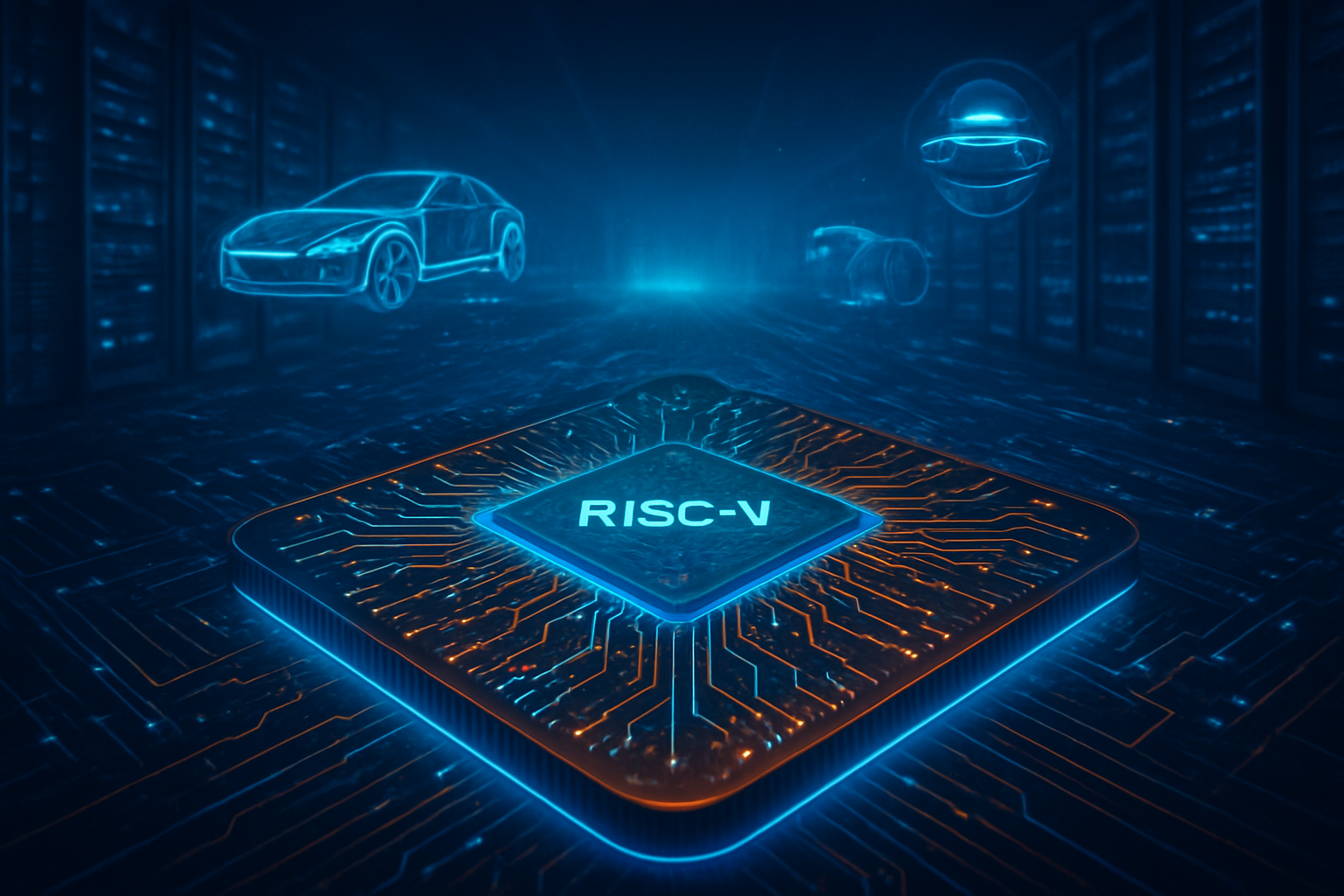
As of January 2026, the electric vehicle (EV) industry has reached a definitive technological tipping point. The era of traditional silicon power electronics is rapidly drawing to a close, replaced by the ascent of Wide-Bandgap (WBG) semiconductors: Silicon Carbide (SiC) and Gallium Nitride (GaN). This transition, once reserved for high-end performance cars, has now moved into the mass market, fundamentally altering the economics of EV ownership by slashing charging times and extending driving ranges to levels previously thought impossible.
The immediate significance of this shift is being amplified by the integration of artificial intelligence into the semiconductor manufacturing process. In early January 2026, the successful deployment of AI-driven predictive modeling in crystal growth furnaces has allowed manufacturers to scale production to unprecedented levels. These developments are not merely incremental; they represent a total reconfiguration of the EV powertrain, enabling 800-volt architectures to become the new global standard for vehicles priced under $40,000, effectively removing the "range anxiety" and "charging lag" that have historically hindered widespread adoption.
The 300mm Revolution: Scaling the Wide-Bandgap Frontier
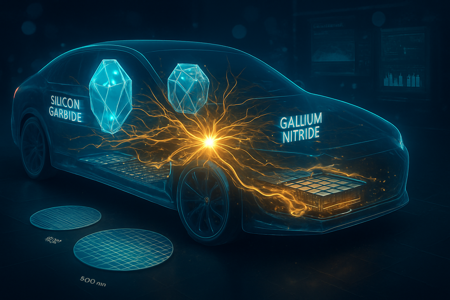
The technical heart of this revolution lies in the physical properties of SiC and GaN. Unlike traditional silicon, these materials have a wider "energy gap," allowing them to operate at much higher voltages, temperatures, and frequencies. In the traction inverter—the part of the EV that converts DC battery power to AC for the motor—SiC MOSFETs have achieved a staggering 99% efficiency rating in 2026. This efficiency reduces energy loss as heat, allowing for smaller cooling systems and a direct 7% to 10% increase in vehicle range. Meanwhile, GaN has become the dominant material for onboard chargers and DC-DC converters, enabling power densities that allow these components to be reduced in size by nearly 50%.
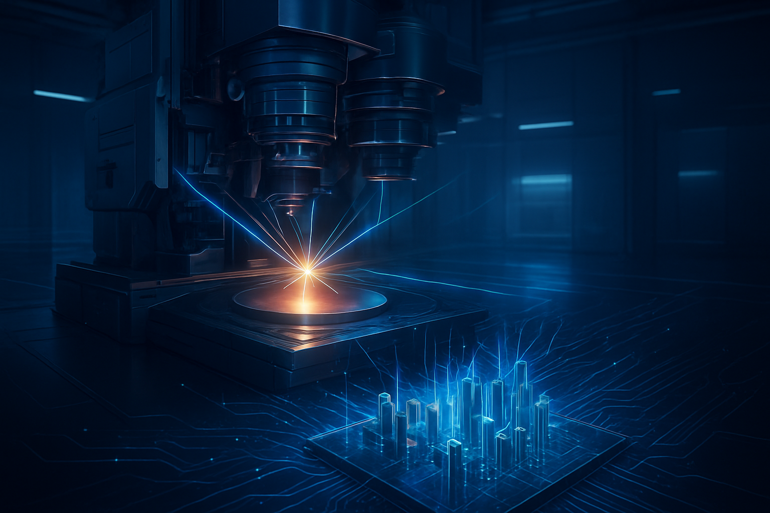
The most significant technical milestone of 2026 occurred on January 13, when Wolfspeed (NYSE: WOLF) announced the production of the world’s first 300mm (12-inch) single-crystal SiC wafer. Historically, SiC manufacturing was limited to 150mm or 200mm wafers due to the extreme difficulty of growing large, defect-free crystals. By utilizing AI-enhanced defect detection and thermal gradient control during the growth process, the industry has finally "scaled the yield wall." This 300mm breakthrough is expected to reduce die costs by up to 40%, finally bringing SiC to price parity with legacy silicon components.
Initial reactions from the research community have been overwhelmingly positive. Analysts at Yole Group have described the 300mm achievement as the "Everest of power electronics," noting that the transition allows for nearly 2.3 times more chips per wafer than the 200mm standard. Industry experts at the Applied Power Electronics Conference (APEC) in January 2026 highlighted that these advancements are no longer just about hardware; they are about "Smart Power." Modern power stages now feature AI-integrated gate drivers that can predict component fatigue months before failure, allowing for predictive maintenance alerts to be delivered directly to the vehicle’s dashboard.
Market Consolidation and the Strategic AI Pivot
The semiconductor landscape has undergone significant consolidation to meet the demands of this 800V era. STMicroelectronics (NYSE: STM) has solidified its position as the volume leader, leveraging a fully vertically integrated supply chain. Their Gen-3 SiC MOSFETs are now the standard for mid-market EVs across Europe and Asia. Following a period of financial restructuring in late 2025, Wolfspeed has emerged as a specialized powerhouse, focusing on the high-yield 300mm production that competitors are now racing to emulate.
The competitive implications are vast for tech giants and startups alike. ON Semiconductor (NASDAQ: ON) has pivoted its strategy toward "EliteSiC" Power Integrated Modules (PIMs), which combine SiC hardware with AI-driven sensing for self-protecting power stages. Meanwhile, Infineon Technologies (OTCMKTS: IFNNY) shocked the market this month by announcing the first high-volume 300mm power GaN production line, a move that positions them to dominate the infrastructure side of the industry, particularly high-speed DC chargers.
This shift is disrupting the traditional automotive supply chain. Legacy Tier-1 suppliers who failed to pivot to WBG materials are seeing their market share eroded by semiconductor-first companies. Furthermore, the partnership between GaN pioneers and AI leaders like NVIDIA (NASDAQ: NVDA) has created a new category of "AI-Optimized Chargers" that can handle the massive power requirements of both EV fleets and AI data centers, creating a synergistic market that benefits companies at the intersection of energy and computation.
The Decarbonization Catalyst: From Infrastructure to Grid Intelligence
Beyond the vehicle itself, the move to SiC and GaN is a critical component of the broader global energy transition. The democratization of 800V systems has paved the way for "Ultra-Fast" charging networks. In 2025, BYD (OTCMKTS: BYDDF) released its Super e-Platform, and by January 2026, it has demonstrated the ability to add 400km of range in just five minutes using SiC-based megawatt chargers. This capability brings the EV refueling experience into direct competition with internal combustion engine (ICE) vehicles, removing the final psychological barrier for many consumers.
However, this rapid charging capability places immense strain on local electrical grids. This is where AI-driven grid intelligence becomes essential. By using AI to orchestrate the "handshake" between the SiC power modules in the car and the GaN-based power stages in the charger, utility companies can balance loads in real-time. This "Smart Power" landscape allows for bidirectional charging (V2G), where EVs act as a distributed battery for the grid, discharging energy during peak demand and charging when renewable energy is most abundant.
The impact of this development is comparable to the introduction of the lithium-ion battery itself. While the battery provides the storage, SiC and GaN provide the "vascular system" that allows that energy to flow efficiently. Some concerns remain regarding the environmental impact of SiC wafer production, which is energy-intensive. However, the 20% yield boost provided by AI manufacturing has already begun to lower the carbon footprint per chip, making the entire lifecycle of the EV significantly greener than models from just three years ago.
The Roadmap to 2030: 1200V Architectures and Beyond
Looking ahead, the next frontier is already visible on the horizon: 1200V architectures. While 800V is the current benchmark for 2026, high-performance trucks, delivery vans, and heavy-duty equipment are expected to migrate toward 1200V by 2028. This will require even more advanced SiC formulations and potentially the introduction of "Diamond" semiconductors, which offer even wider bandgaps than SiC.
In the near term, expect to see the "miniaturization" of the drivetrain. As AI continues to optimize switching frequencies, we will likely see "all-in-one" drive units where the motor, inverter, and gearbox are integrated into a single, compact module no larger than a carry-on suitcase. Challenges remain in the global supply of raw materials like high-purity carbon and gallium, but experts predict that the opening of new domestic refining facilities in North America and Europe by 2027 will alleviate these bottlenecks.
The integration of solid-state batteries, expected to hit the market in limited volumes by late 2027, will further benefit from SiC power electronics. The high thermal stability of SiC is a perfect match for the higher operating temperatures of some solid-state chemistries. Experts predict that the combination of SiC/GaN power stages and solid-state batteries will lead to "thousand-mile" EVs by the end of the decade.
Conclusion: The New Standard of Electric Mobility
The shift to Silicon Carbide and Gallium Nitride, supercharged by AI manufacturing and real-time power management, represents the most significant advancement in EV technology this decade. As of January 2026, we have moved past the "early adopter" phase and into an era where electric mobility is defined by efficiency, speed, and intelligence. The 300mm wafer breakthrough and the 800V standard have effectively leveled the playing field between electric and gasoline vehicles.
For the tech industry and society at large, the key takeaway is that the "silicon" in Silicon Valley is no longer the only game in town. The future of energy is wide-bandgap. In the coming weeks, watch for further announcements from Tesla (NASDAQ: TSLA) regarding their next-generation "Unboxed" manufacturing process, which is rumored to rely heavily on the new AI-optimized SiC modules. The road to 2030 is electric, and it is being paved with SiC and GaN.
This content is intended for informational purposes only and represents analysis of current AI developments.
TokenRing AI delivers enterprise-grade solutions for multi-agent AI workflow orchestration, AI-powered development tools, and seamless remote collaboration platforms.
For more information, visit https://www.tokenring.ai/.