San Jose, CA & San Francisco, CA – October 13, 2025 – In a landmark development set to reshape the artificial intelligence and semiconductor landscapes, Broadcom Inc. (NASDAQ: AVGO) and OpenAI have announced a multi-billion dollar strategic collaboration. This ambitious partnership focuses on the co-development and deployment of an unprecedented 10 gigawatts of custom AI accelerators, signaling a pivotal shift towards specialized hardware tailored for frontier AI models. The deal, which sees OpenAI designing the specialized AI chips and systems in conjunction with Broadcom's development and deployment expertise, is slated to commence deployment in the latter half of 2026 and conclude by the end of 2029.
OpenAI's foray into co-designing its own accelerators stems from a strategic imperative to embed insights gleaned from the development of its advanced AI models directly into the hardware. This proactive approach aims to unlock new levels of capability, intelligence, and efficiency, ultimately driving down compute costs and enabling the delivery of faster, more efficient, and more affordable AI. For the semiconductor sector, the agreement significantly elevates Broadcom's position as a critical player in the AI hardware domain, particularly in custom accelerators and high-performance Ethernet networking solutions, solidifying its status as a formidable competitor in the accelerated computing race. The immediate aftermath of the announcement saw Broadcom's shares surge, reflecting robust investor confidence in its expanding strategic importance within the burgeoning AI infrastructure market.
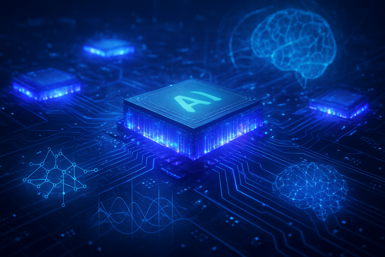
Engineering the Future of AI: Custom Silicon and Unprecedented Scale
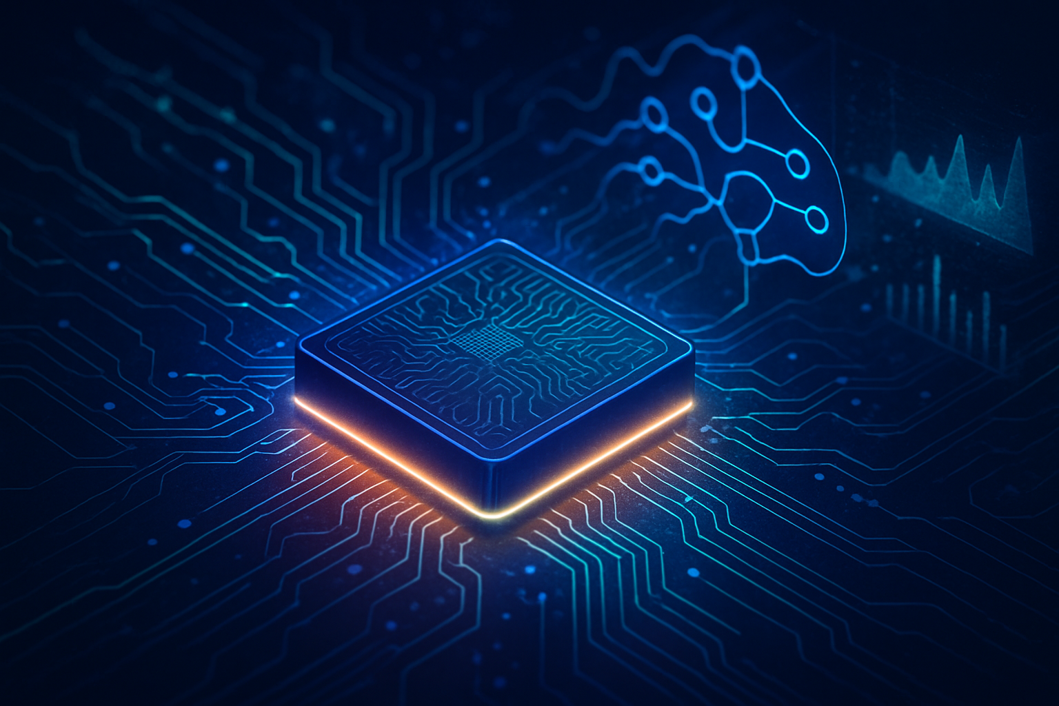
The core of the Broadcom-OpenAI deal revolves around the co-development and deployment of custom AI accelerators designed specifically for OpenAI's demanding workloads. While specific technical specifications of the chips themselves remain proprietary, the overarching goal is to create hardware that is intimately optimized for the architecture of OpenAI's large language models and other frontier AI systems. This bespoke approach allows OpenAI to tailor every aspect of the chip – from its computational units to its memory architecture and interconnects – to maximize the performance and efficiency of its software, a level of optimization not typically achievable with off-the-shelf general-purpose GPUs.
This initiative represents a significant departure from the traditional model where AI developers primarily rely on standard, high-volume GPUs from established providers like Nvidia. By co-designing its own inference chips, OpenAI is taking a page from hyperscalers like Google and Amazon, who have successfully developed custom silicon (TPUs and Inferentia, respectively) to gain a competitive edge in AI. The partnership with Broadcom, renowned for its expertise in custom silicon (ASICs) and high-speed networking, provides the necessary engineering prowess and manufacturing connections to bring these designs to fruition. Broadcom's role extends beyond mere fabrication; it encompasses the development of the entire accelerator rack, integrating its advanced Ethernet and other connectivity solutions to ensure seamless, high-bandwidth communication within and between the massive clusters of AI chips. This integrated approach is crucial for achieving the 10 gigawatts of computing power, a scale that dwarfs most existing AI deployments and underscores the immense demands of next-generation AI. Initial reactions from the AI research community highlight the strategic necessity of such vertical integration, with experts noting that custom hardware is becoming indispensable for pushing the boundaries of AI performance and cost-effectiveness.
Reshaping the Competitive Landscape: Winners, Losers, and Strategic Shifts
The Broadcom-OpenAI deal sends significant ripples through the AI and semiconductor industries, reconfiguring competitive dynamics and strategic positioning. OpenAI stands to be a primary beneficiary, gaining unparalleled control over its AI infrastructure. This vertical integration allows the company to reduce its dependency on external chip suppliers, potentially lowering operational costs, accelerating innovation cycles, and ensuring a stable, optimized supply of compute power essential for its ambitious growth plans, including CEO Sam Altman's vision to expand computing capacity to 250 gigawatts by 2033. This strategic move strengthens OpenAI's ability to deliver faster, more efficient, and more affordable AI models, potentially solidifying its market leadership in generative AI.
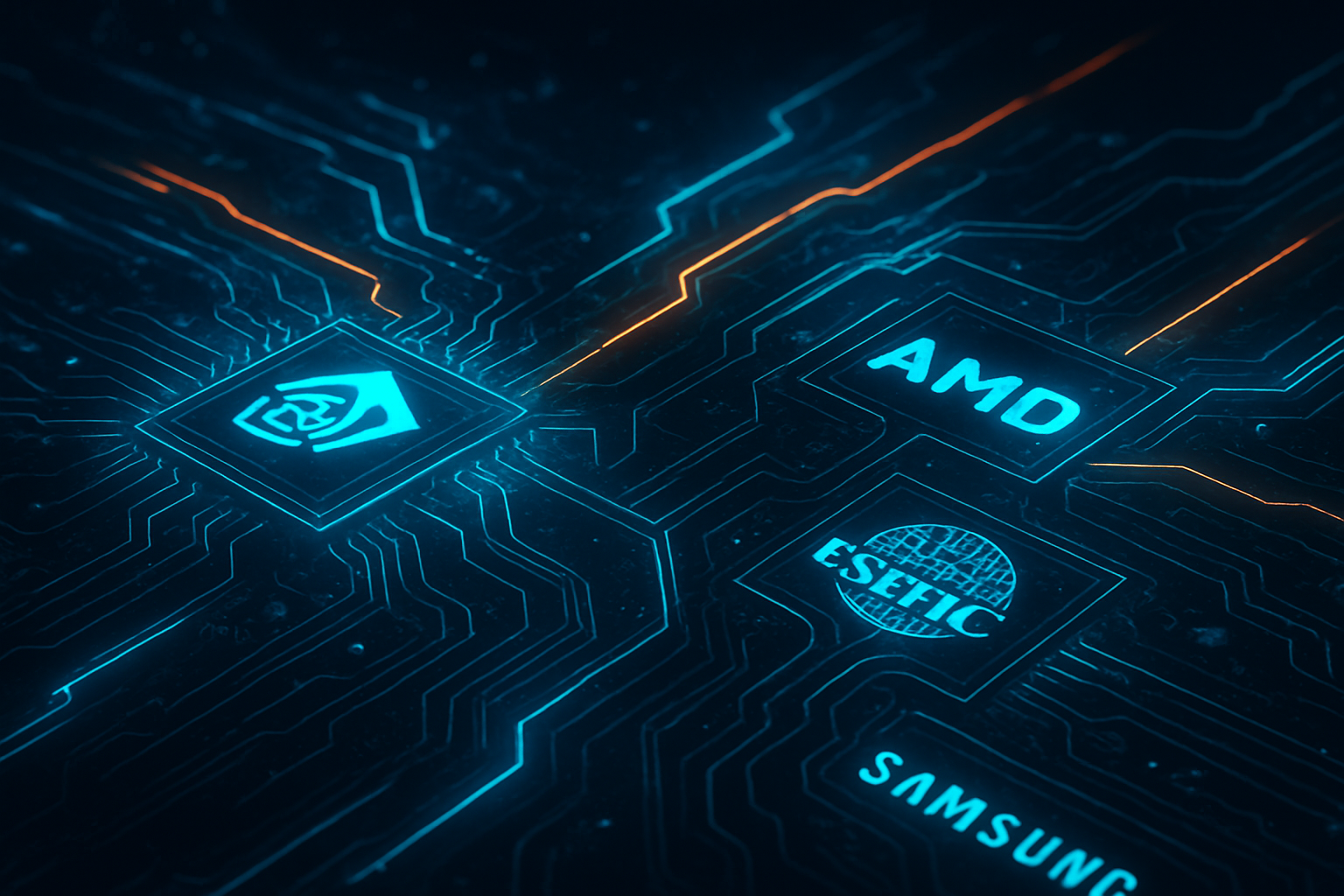
For Broadcom (NASDAQ: AVGO), the partnership is a monumental win. It significantly elevates the company's standing in the fiercely competitive AI hardware market, positioning it as a critical enabler of frontier AI. Broadcom's expertise in custom ASICs and high-performance networking solutions, particularly its Ethernet technology, is now directly integrated into one of the world's leading AI labs' core infrastructure. This deal not only diversifies Broadcom's revenue streams but also provides a powerful endorsement of its capabilities, making it a formidable competitor to other chip giants like Nvidia (NASDAQ: NVDA) and Advanced Micro Devices (NASDAQ: AMD) in the custom AI accelerator space. The competitive implications for major AI labs and tech companies are profound. While Nvidia remains a dominant force, OpenAI's move signals a broader trend among major AI players to explore custom silicon, which could lead to a diversification of chip demand and increased competition for Nvidia in the long run. Companies like Google (NASDAQ: GOOGL) and Amazon (NASDAQ: AMZN) with their own custom AI chips may see this as validation of their strategies, while others might feel pressure to pursue similar vertical integration to maintain parity. The deal could also disrupt existing product cycles, as the availability of highly optimized custom hardware may render some general-purpose solutions less competitive for specific AI workloads, forcing chipmakers to innovate faster and offer more tailored solutions.
A New Era of AI Infrastructure: Broader Implications and Future Trajectories
This collaboration between Broadcom and OpenAI marks a significant inflection point in the broader AI landscape, signaling a maturation of the industry where hardware innovation is becoming as critical as algorithmic breakthroughs. It underscores a growing trend of "AI factories" – large-scale, highly specialized data centers designed from the ground up to train and deploy advanced AI models. This deal fits into the broader narrative of AI companies seeking greater control and efficiency over their compute infrastructure, moving beyond generic hardware to purpose-built systems. The impacts are far-reaching: it will likely accelerate the development of more powerful and complex AI models by removing current hardware bottlenecks, potentially leading to breakthroughs in areas like scientific discovery, personalized medicine, and autonomous systems.
However, this trend also raises potential concerns. The immense capital expenditure required for such custom hardware initiatives could further concentrate power within a few well-funded AI entities, potentially creating higher barriers to entry for startups. It also highlights the environmental impact of AI, as 10 gigawatts of computing power represents a substantial energy demand, necessitating continued innovation in energy efficiency and sustainable data center practices. Comparisons to previous AI milestones, such as the rise of GPUs for deep learning or the development of specialized cloud AI services, reveal a consistent pattern: as AI advances, so too does the need for specialized infrastructure. This deal represents the next logical step in that evolution, moving from off-the-shelf acceleration to deeply integrated, co-designed systems. It signifies that the future of frontier AI will not just be about smarter algorithms, but also about the underlying silicon and networking that brings them to life.
The Horizon of AI: Expected Developments and Expert Predictions
Looking ahead, the Broadcom-OpenAI deal sets the stage for several significant developments in the near-term and long-term. In the near-term (2026-2029), we can expect to see the gradual deployment of these custom AI accelerator racks, leading to a demonstrable increase in the efficiency and performance of OpenAI's models. This will likely manifest in faster training times, lower inference costs, and the ability to deploy even larger and more complex AI systems. We might also see a "halo effect" where other major AI players, witnessing the benefits of vertical integration, intensify their efforts to develop or procure custom silicon solutions, further fragmenting the AI chip market. The deal's success could also spur innovation in related fields, such as advanced cooling technologies and power management solutions, essential for handling the immense energy demands of 10 gigawatts of compute.
In the long-term, the implications are even more profound. The ability to tightly couple AI software and hardware could unlock entirely new AI capabilities and applications. We could see the emergence of highly specialized AI models designed exclusively for these custom architectures, pushing the boundaries of what's possible in areas like real-time multimodal AI, advanced robotics, and highly personalized intelligent agents. However, significant challenges remain. Scaling such massive infrastructure while maintaining reliability, security, and cost-effectiveness will be an ongoing engineering feat. Moreover, the rapid pace of AI innovation means that even custom hardware can become obsolete quickly, necessitating agile design and deployment cycles. Experts predict that this deal is a harbinger of a future where AI companies become increasingly involved in hardware design, blurring the lines between software and silicon. They anticipate a future where AI capabilities are not just limited by algorithms, but by the physical limits of computation, making hardware optimization a critical battleground for AI leadership.
A Defining Moment for AI and Semiconductors
The Broadcom-OpenAI deal is undeniably a defining moment in the history of artificial intelligence and the semiconductor industry. It encapsulates a strategic imperative for leading AI developers to gain greater control over their foundational compute infrastructure, moving beyond reliance on general-purpose hardware to purpose-built, highly optimized custom silicon. The sheer scale of the announced 10 gigawatts of computing power underscores the insatiable demand for AI capabilities and the unprecedented resources required to push the boundaries of frontier AI. Key takeaways include OpenAI's bold step towards vertical integration, Broadcom's ascendancy as a pivotal player in custom AI accelerators and networking, and the broader industry shift towards specialized hardware for next-generation AI.
This development's significance in AI history cannot be overstated; it marks a transition from an era where AI largely adapted to existing hardware to one where hardware is explicitly designed to serve the escalating demands of AI. The long-term impact will likely see accelerated AI innovation, increased competition in the chip market, and potentially a more fragmented but highly optimized AI infrastructure landscape. In the coming weeks and months, industry observers will be watching closely for more details on the chip architectures, the initial deployment milestones, and how competitors react to this powerful new alliance. This collaboration is not just a business deal; it is a blueprint for the future of AI at scale, promising to unlock capabilities that were once only theoretical.
This content is intended for informational purposes only and represents analysis of current AI developments.
TokenRing AI delivers enterprise-grade solutions for multi-agent AI workflow orchestration, AI-powered development tools, and seamless remote collaboration platforms.
For more information, visit https://www.tokenring.ai/.