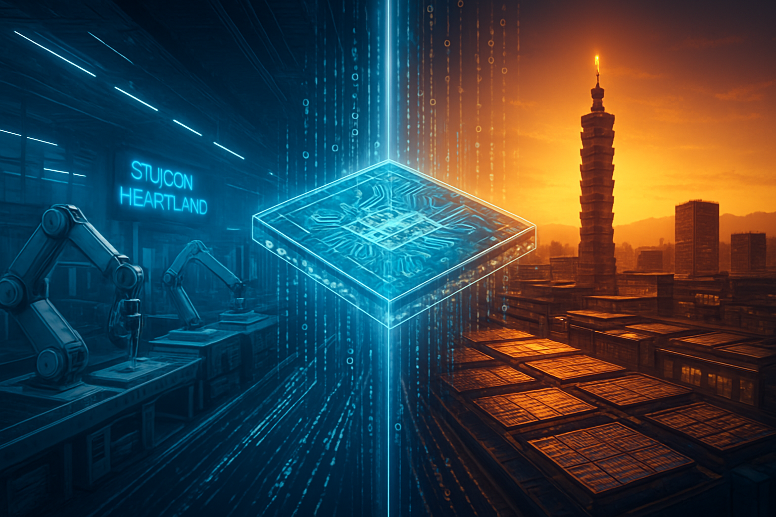
As of January 27, 2026, the global semiconductor landscape has reached a pivotal inflection point. China’s tech titans are no longer content with merely consuming hardware; they are now manufacturing the very bedrock of the AI revolution. Recent reports indicate that both Alibaba Group Holding Ltd (NYSE: BABA / HKG: 9988) and Baidu, Inc. (NASDAQ: BIDU / HKG: 9888) are accelerating plans to spin off their respective chip-making units—T-Head (PingTouGe) and Kunlunxin—into independent, publicly traded entities. This strategic pivot marks the most aggressive challenge yet to the long-standing hegemony of traditional silicon giants like NVIDIA Corporation (NASDAQ: NVDA) and Advanced Micro Devices, Inc. (NASDAQ: AMD).
The significance of these potential IPOs cannot be overstated. By transitioning their internal chip divisions into commercial "merchant" vendors, Alibaba and Baidu are signaling a move toward market-wide distribution of their proprietary silicon. This development directly addresses the growing demand for AI compute within China, where access to high-end Western chips remains restricted by evolving export controls. For the broader tech industry, this represents the crystallization of "Item 5" on the annual list of defining AI trends: the rise of in-house hyperscaler silicon as a primary driver of regional self-reliance and geopolitical tech-decoupling.
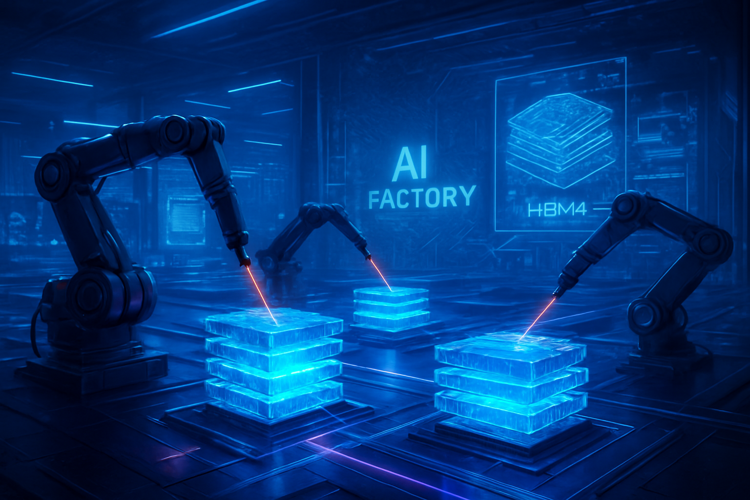
The Technical Vanguard: P800s, Yitians, and the RISC-V Revolution
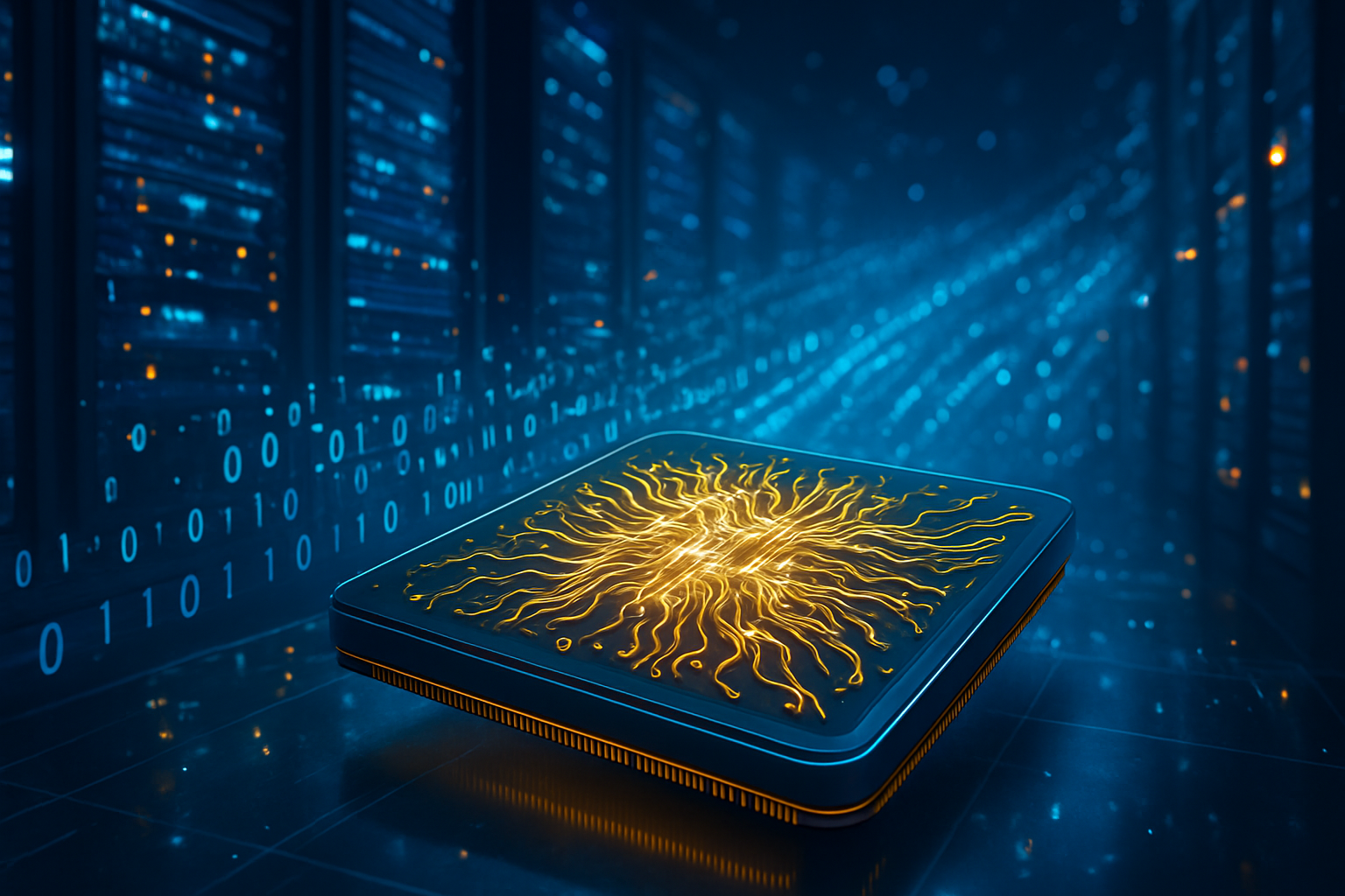
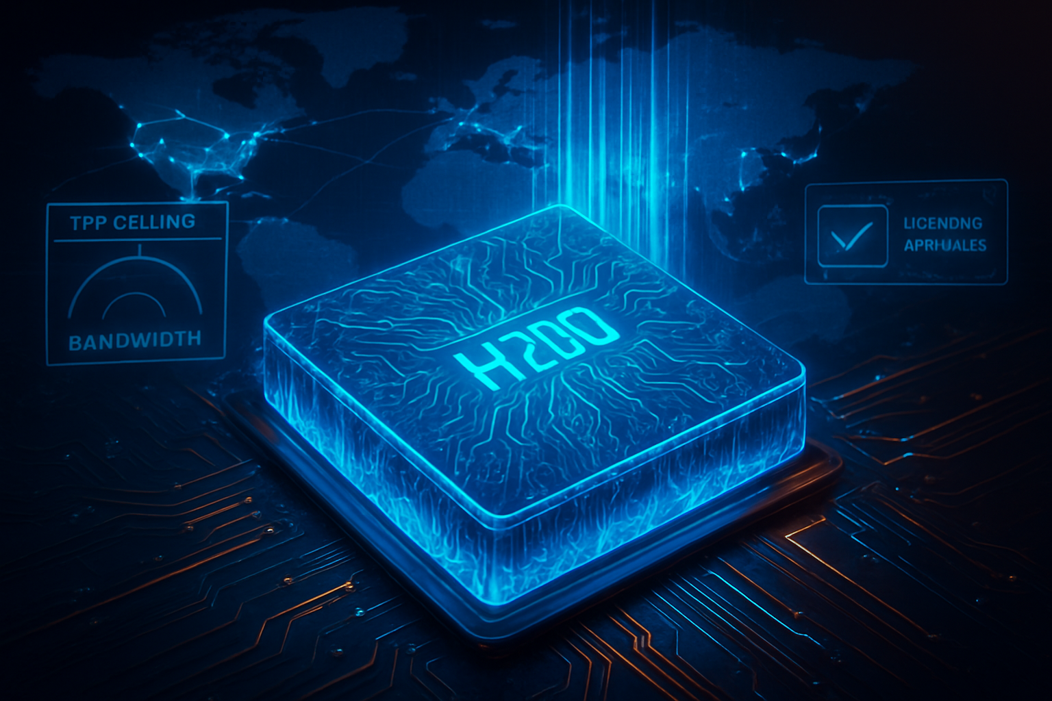
The technical achievements coming out of T-Head and Kunlunxin have evolved from experimental prototypes to production-grade powerhouses. Baidu’s Kunlunxin recently entered mass production for its Kunlun 3 (P800) series. Built on a 7nm process, the P800 is specifically optimized for Baidu’s Ernie 5.0 large language model, featuring advanced 8-bit inference capabilities and support for the emerging Mixture of Experts (MoE) architectures. Initial benchmarks suggest that the P800 is not just a domestic substitute; it actively competes with the NVIDIA H20—a chip specifically designed by NVIDIA to comply with U.S. sanctions—by offering superior memory bandwidth and specialized interconnects designed for 30,000-unit clusters.
Meanwhile, Alibaba’s T-Head division has focused on a dual-track strategy involving both Arm-based and RISC-V architectures. The Yitian 710, Alibaba’s custom server CPU, has established itself as one of the fastest Arm-based processors in the cloud market, reportedly outperforming mainstream offerings from Intel Corporation (NASDAQ: INTC) in specific database and cloud-native workloads. More critically, T-Head’s XuanTie C930 processor represents a breakthrough in RISC-V development, offering a high-performance alternative to Western instruction set architectures (ISAs). By championing RISC-V, Alibaba is effectively "future-proofing" its silicon roadmap against further licensing restrictions that could impact Arm or x86 technologies.
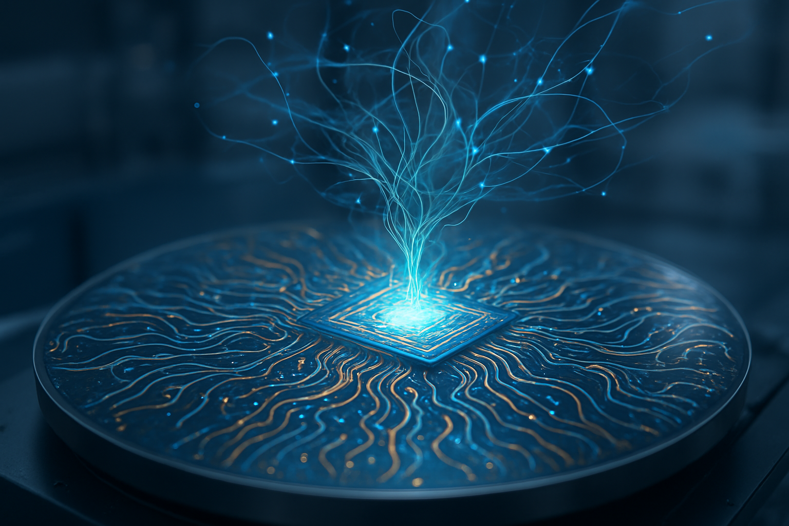
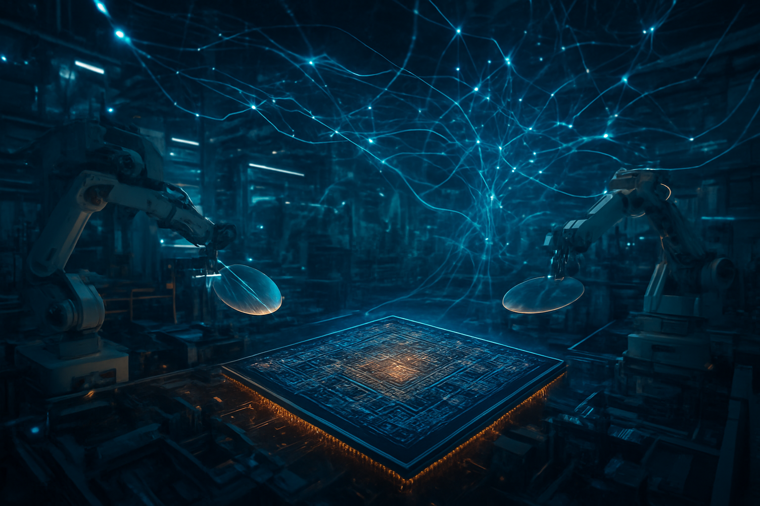
Industry experts have noted that the "secret sauce" of these in-house designs lies in their tight integration with the parent companies’ software stacks. Unlike general-purpose GPUs, which must accommodate a vast array of use cases, Kunlunxin and T-Head chips are co-designed with the specific requirements of the Ernie and Qwen models in mind. This "vertical integration" allows for radical efficiencies in power consumption and data throughput, effectively closing the performance gap created by the lack of access to 3nm or 2nm fabrication technologies currently held by global leaders like TSMC.
Disruption of the "NVIDIA Tax" and the Merchant Model
The move toward an IPO serves a critical strategic purpose: it allows these units to sell their chips to external competitors and state-owned enterprises, transforming them from cost centers into profit-generating powerhouses. This shift is already beginning to erode NVIDIA’s dominance in the Chinese market. Analyst projections for early 2026 suggest that NVIDIA’s market share in China could plummet to single digits, a staggering decline from over 60% just three years ago. As Kunlunxin and T-Head scale their production, they are increasingly able to offer domestic clients a "plug-and-play" alternative that avoids the premium pricing and supply chain volatility associated with Western imports.
For the parent companies, the benefits are two-fold. First, they dramatically reduce their internal capital expenditure—often referred to as the "NVIDIA tax"—by using their own silicon to power their massive cloud infrastructures. Second, the injection of capital from public markets will provide the multi-billion dollar R&D budgets required to compete at the bleeding edge of semiconductor physics. This creates a feedback loop where the success of the chip units subsidizes the AI training costs of the parent companies, giving Alibaba and Baidu a formidable strategic advantage over domestic rivals who must still rely on third-party hardware.
However, the implications extend beyond China’s borders. The success of T-Head and Kunlunxin provides a blueprint for other global hyperscalers. While companies like Amazon.com, Inc. (NASDAQ: AMZN) and Alphabet Inc. (NASDAQ: GOOGL) have long used custom silicon (Graviton and TPU, respectively), the Alibaba and Baidu model of spinning these units off into commercial entities could force a rethink of how cloud providers view their hardware assets. We are entering an era where the world’s largest software companies are becoming the world’s most influential hardware designers.
Silicon Sovereignty and the New Geopolitical Landscape
The rise of these in-house chip units is inextricably linked to China’s broader push for "Silicon Sovereignty." Under the current 15th Five-Year Plan, Beijing has placed unprecedented emphasis on achieving a 50% self-sufficiency rate in semiconductors. Alibaba and Baidu have effectively been drafted as "national champions" in this effort. The reported IPO plans are not just financial maneuvers; they are part of a coordinated effort to insulate China’s AI ecosystem from external shocks. By creating a self-sustaining domestic market for AI silicon, these companies are building a "Great Firewall" of hardware that is increasingly difficult for international regulations to penetrate.
This trend mirrors the broader global shift toward specialized silicon, which we have identified as a defining characteristic of the mid-2020s AI boom. The era of the general-purpose chip is giving way to an era of "bespoke compute." When a hyperscaler builds its own silicon, it isn't just seeking to save money; it is seeking to define the very parameters of what its AI can achieve. The technical specifications of the Kunlun 3 and the XuanTie C930 are reflections of the specific AI philosophies of Baidu and Alibaba, respectively.
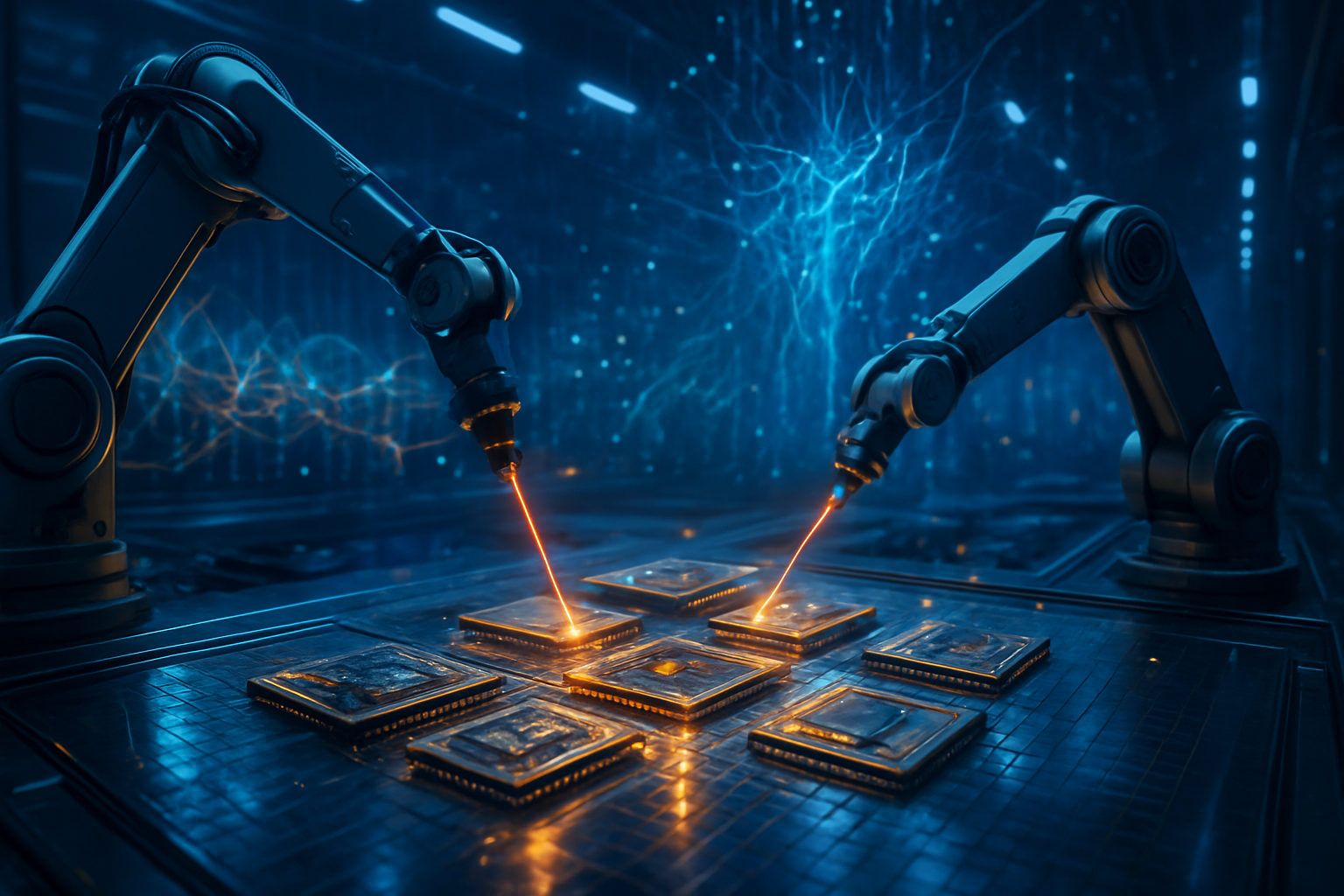
Potential concerns remain, particularly regarding the sustainability of the domestic supply chain. While design capabilities have surged, the reliance on domestic foundries like SMIC for 7nm and 5nm production remains a potential bottleneck. The IPOs of Kunlunxin and T-Head will be a litmus test for whether private capital is willing to bet on China’s ability to overcome these manufacturing hurdles. If successful, these listings will represent a landmark moment in AI history, proving that specialized, in-house design can successfully challenge the dominance of a trillion-dollar incumbent like NVIDIA.
The Horizon: Multi-Agent Workflows and Trillion-Parameter Scaling
Looking ahead, the next phase for T-Head and Kunlunxin involves scaling their hardware to meet the demands of trillion-parameter multimodal models and sophisticated multi-agent AI workflows. Baidu’s roadmap for the Kunlun M300, expected in late 2026 or 2027, specifically targets the massive compute requirements of Mixture of Experts (MoE) models that require lightning-fast interconnects between thousands of individual chips. Similarly, Alibaba is expected to expand its XuanTie RISC-V lineup into the automotive and edge computing sectors, creating a ubiquitous ecosystem of "PingTouGe-powered" devices.
One of the most significant challenges on the horizon will be software compatibility. While Baidu has claimed significant progress in creating CUDA-compatible layers for its chips—allowing developers to migrate from NVIDIA with minimal code changes—the long-term goal is to establish a native domestic ecosystem. If T-Head and Kunlunxin can convince a generation of Chinese developers to build natively for their architectures, they will have achieved a level of platform lock-in that transcends mere hardware performance.
Experts predict that the success of these IPOs will trigger a wave of similar spinoffs across the tech sector. We may soon see specialized AI silicon units from other major players seeking independent listings as the "hyperscaler silicon" trend moves into high gear. The coming months will be critical as Kunlunxin moves through its filing process in Hong Kong, providing the first real-world valuation of a "hyperscaler-born" commercial chip vendor.
Conclusion: A New Era of Decentralized Compute
The reported IPO plans for Alibaba’s T-Head and Baidu’s Kunlunxin represent a seismic shift in the AI industry. What began as internal R&D projects to solve local supply problems have evolved into sophisticated commercial operations capable of disrupting the global semiconductor order. This development validates the rise of in-house hyperscaler silicon as a primary driver of innovation, shifting the balance of power from traditional chipmakers to the cloud giants who best understand the needs of modern AI.
As we move further into 2026, the key takeaway is that silicon independence is no longer a luxury for the tech elite; it is a strategic necessity. The significance of this moment in AI history lies in the decentralization of high-performance compute. By successfully commercializing their internal designs, Alibaba and Baidu are proving that the future of AI will be built on foundation-specific hardware. Investors and industry watchers should keep a close eye on the Hong Kong and Shanghai markets in the coming weeks, as the financial debut of these units will likely set the tone for the next decade of semiconductor competition.
This content is intended for informational purposes only and represents analysis of current AI developments.
TokenRing AI delivers enterprise-grade solutions for multi-agent AI workflow orchestration, AI-powered development tools, and seamless remote collaboration platforms.
For more information, visit https://www.tokenring.ai/.