Tag: Semiconductors

  • Unlocking the AI Revolution: Advanced Packaging Propels Next-Gen Chips Beyond Moore’s Law

    Unlocking the AI Revolution: Advanced Packaging Propels Next-Gen Chips Beyond Moore’s Law

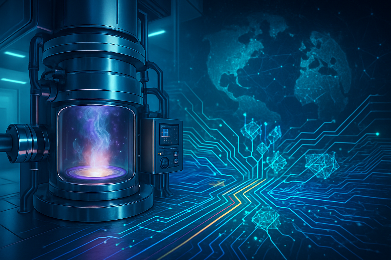
    The relentless pursuit of more powerful, efficient, and compact artificial intelligence (AI) systems has pushed the semiconductor industry to the brink of traditional scaling limits. As the era of simply shrinking transistors on a 2D plane becomes increasingly challenging and costly, a new paradigm in chip design and manufacturing is taking center stage: advanced packaging technologies. These groundbreaking innovations are no longer mere afterthoughts in the chip-making process; they are now the critical enablers for unlocking the true potential of AI, fundamentally reshaping how AI chips are built and perform.

    These sophisticated packaging techniques are immediately significant because they directly address the most formidable bottlenecks in AI hardware, particularly the infamous "memory wall." By allowing for unprecedented levels of integration between processing units and high-bandwidth memory, advanced packaging dramatically boosts data transfer rates, slashes latency, and enables a much higher computational density. This paradigm shift is not just an incremental improvement; it is a foundational leap that will empower the development of more complex, power-efficient, and smaller AI devices, from edge computing to hyperscale data centers, thereby fueling the next wave of AI breakthroughs.

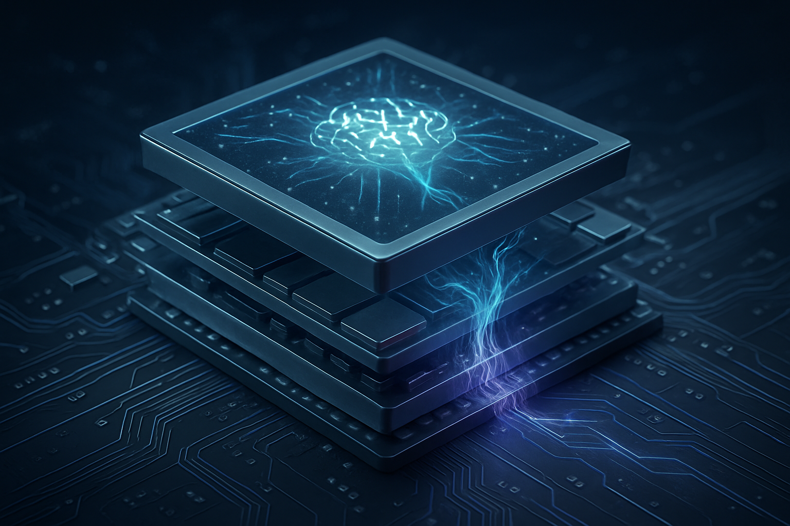
    The Technical Core: Engineering AI's Performance Edge

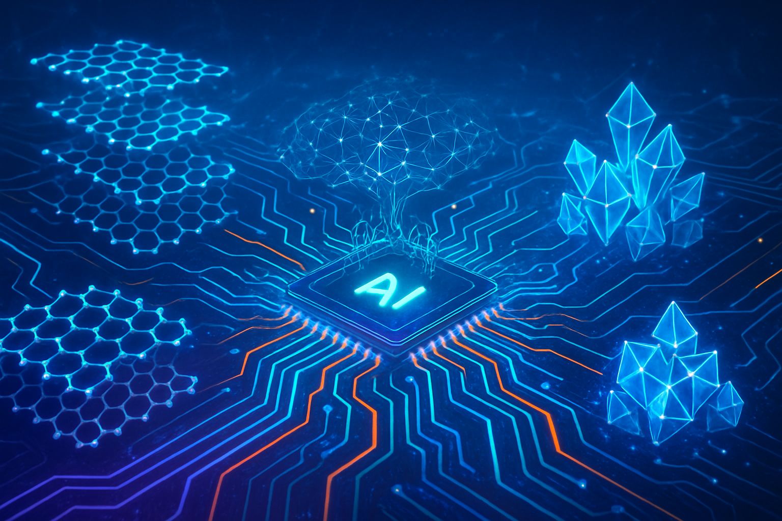
    The advancements in semiconductor packaging represent a diverse toolkit, each method offering unique advantages for enhancing AI chip capabilities. These innovations move beyond traditional 2D integration, which places components side-by-side on a single substrate, by enabling vertical stacking and heterogeneous integration.

    2.5D Packaging (e.g., CoWoS, EMIB): This approach, pioneered by companies like TSMC (NYSE: TSM) with its CoWoS (Chip-on-Wafer-on-Substrate) and Intel (NASDAQ: INTC) with EMIB (Embedded Multi-die Interconnect Bridge), involves placing multiple bare dies, such as a GPU and High-Bandwidth Memory (HBM) stacks, on a shared silicon or organic interposer. The interposer acts as a high-speed communication bridge, drastically shortening signal paths between logic and memory. This provides an ultra-wide communication bus, crucial for data-intensive AI workloads, effectively mitigating the "memory wall" problem and enabling higher throughput for AI model training and inference. Compared to traditional package-on-package (PoP) or system-in-package (SiP) solutions with longer traces, 2.5D offers superior bandwidth and lower latency.

    3D Stacking and Through-Silicon Vias (TSVs): Representing a true vertical integration, 3D stacking involves placing multiple active dies or wafers directly atop one another. The enabling technology here is Through-Silicon Vias (TSVs) – vertical electrical connections that pass directly through the silicon dies, facilitating direct communication and power transfer between layers. This offers unparalleled bandwidth and even lower latency than 2.5D solutions, as signals travel minimal distances. The primary difference from 2.5D is the direct vertical connection, allowing for significantly higher integration density and more powerful AI hardware within a smaller footprint. While thermal management is a challenge due to increased density, innovations in microfluidic cooling are being developed to address this.

    Hybrid Bonding: This cutting-edge 3D packaging technique facilitates direct copper-to-copper (Cu-Cu) connections at the wafer or die-to-wafer level, bypassing traditional solder bumps. Hybrid bonding achieves ultra-fine interconnect pitches, often in the single-digit micrometer range, a significant improvement over conventional microbump technology. This results in ultra-dense interconnects and bandwidths up to 1000 GB/s, bolstering signal integrity and efficiency. For AI, this means even shorter signal paths, lower parasitic resistance and capacitance, and ultimately, more efficient and compact HBM stacks crucial for memory-bound AI accelerators.

    Chiplet Technology: Instead of a single, large monolithic chip, chiplet technology breaks down a system into several smaller, functional integrated circuits (ICs), or "chiplets," each optimized for a specific task. These chiplets (e.g., CPU, GPU, memory, AI accelerators) are then interconnected within a single package. This modular approach supports heterogeneous integration, allowing different functions to be fabricated on their most optimal process node (e.g., compute cores on 3nm, I/O dies on 7nm). This not only improves overall energy efficiency by 30-40% for the same workload but also allows for performance scalability, specialization, and overcomes the physical limitations (reticle limits) of monolithic die size. Initial reactions from the AI research community highlight chiplets as a game-changer for custom AI hardware, enabling faster iteration and specialized designs.

    Fan-Out Packaging (FOWLP/FOPLP): Fan-out packaging eliminates the need for traditional package substrates by embedding dies directly into a molding compound, allowing for more I/O connections in a smaller footprint. Fan-out Panel-Level Packaging (FOPLP) is an advanced variant that reassembles chips on a larger panel instead of a wafer, enabling higher throughput and lower cost. These methods provide higher I/O density, improved signal integrity due to shorter electrical paths, and better thermal performance, all while significantly reducing the package size.

    Reshaping the AI Industry Landscape

    These advancements in advanced packaging are creating a significant ripple effect across the AI industry, poised to benefit established tech giants and innovative startups alike, while also intensifying competition. Companies that master these technologies will gain substantial strategic advantages.

    Key Beneficiaries and Competitive Implications: Semiconductor foundries like TSMC (NYSE: TSM) are at the forefront, with their CoWoS platform being critical for high-performance AI accelerators from NVIDIA (NASDAQ: NVDA) and AMD (NASDAQ: AMD). NVIDIA's dominance in AI hardware is heavily reliant on its ability to integrate powerful GPUs with HBM using TSMC's advanced packaging. Intel (NASDAQ: INTC), with its EMIB and Foveros 3D stacking technologies, is aggressively pursuing a leadership position in heterogeneous integration, aiming to offer competitive AI solutions that combine various compute tiles. Samsung (KRX: 005930), a major player in both memory and foundry, is investing heavily in hybrid bonding and 3D packaging to enhance its HBM products and offer integrated solutions for AI chips. AMD (NASDAQ: AMD) leverages chiplet architectures extensively in its CPUs and GPUs, enabling competitive performance and cost structures for AI workloads.

    Disruption and Strategic Advantages: The ability to densely integrate specialized AI accelerators, memory, and I/O within a single package will disrupt traditional monolithic chip design. Startups focused on domain-specific AI architectures can leverage chiplets and advanced packaging to rapidly prototype and deploy highly optimized solutions, challenging the one-size-fits-all approach. Companies that can effectively design for and utilize these packaging techniques will gain significant market positioning through superior performance-per-watt, smaller form factors, and potentially lower costs at scale due to improved yields from smaller chiplets. The strategic advantage lies not just in manufacturing prowess but also in the design ecosystem that can effectively utilize these complex integration methods.

    The Broader AI Canvas: Impacts and Concerns

    The emergence of advanced packaging as a cornerstone of AI hardware development marks a pivotal moment, fitting perfectly into the broader trend of specialized hardware acceleration for AI. This is not merely an evolutionary step but a fundamental shift that underpins the continued exponential growth of AI capabilities.

    Impacts on the AI Landscape: These packaging breakthroughs enable the creation of AI systems that are orders of magnitude more powerful and efficient than what was previously possible. This directly translates to the ability to train larger, more complex deep learning models, accelerate inference at the edge, and deploy AI in power-constrained environments like autonomous vehicles and advanced robotics. The higher bandwidth and lower latency facilitate real-time processing of massive datasets, crucial for applications like generative AI, large language models, and advanced computer vision. It also democratizes access to high-performance AI, as smaller, more efficient packages can be integrated into a wider range of devices.

    Potential Concerns: While the benefits are immense, challenges remain. The complexity of designing and manufacturing these multi-die packages is significantly higher than traditional chips, leading to increased design costs and potential yield issues. Thermal management in 3D-stacked chips is a persistent concern, as stacking multiple heat-generating layers can lead to hotspots and performance degradation if not properly addressed. Furthermore, the interoperability and standardization of chiplet interfaces are critical for widespread adoption and could become a bottleneck if not harmonized across the industry.

    Comparison to Previous Milestones: These advancements can be compared to the introduction of multi-core processors or the widespread adoption of GPUs for general-purpose computing. Just as those innovations unlocked new computational paradigms, advanced packaging is enabling a new era of heterogeneous integration and specialized AI acceleration, moving beyond the limitations of Moore's Law and ensuring that the physical hardware can keep pace with the insatiable demands of AI software.

    The Horizon: Future Developments in Packaging for AI

    The current innovations in advanced packaging are just the beginning. The coming years promise even more sophisticated integration techniques that will further push the boundaries of AI hardware, enabling new applications and solving existing challenges.

    Expected Near-Term and Long-Term Developments: We can expect a continued evolution of hybrid bonding to achieve even finer pitches and higher interconnect densities, potentially leading to true monolithic 3D integration where logic and memory are seamlessly interwoven at the transistor level. Research is ongoing into novel materials and processes for TSVs to improve density and reduce resistance. The standardization of chiplet interfaces, such as UCIe (Universal Chiplet Interconnect Express), is crucial and will accelerate the modular design of AI systems. Long-term, we might see the integration of optical interconnects within packages to overcome electrical signaling limits, offering unprecedented bandwidth and power efficiency for inter-chiplet communication.

    Potential Applications and Use Cases: These advancements will have a profound impact across the AI spectrum. In data centers, more powerful and efficient AI accelerators will drive the next generation of large language models and generative AI, enabling faster training and inference with reduced energy consumption. At the edge, compact and low-power AI chips will power truly intelligent IoT devices, advanced robotics, and highly autonomous systems, bringing sophisticated AI capabilities directly to the point of data generation. Medical devices, smart cities, and personalized AI assistants will all benefit from the ability to embed powerful AI in smaller, more efficient packages.

    Challenges and Expert Predictions: Key challenges include managing the escalating costs of advanced packaging R&D and manufacturing, ensuring robust thermal dissipation in highly dense packages, and developing sophisticated design automation tools capable of handling the complexity of heterogeneous 3D integration. Experts predict a future where the "system-on-chip" evolves into a "system-in-package," with optimized chiplets from various vendors seamlessly integrated to create highly customized AI solutions. The emphasis will shift from maximizing transistor count on a single die to optimizing the interconnections and synergy between diverse functional blocks.

    A New Era of AI Hardware: The Integrated Future

    The rapid advancements in advanced packaging technologies for semiconductors mark a pivotal moment in the history of artificial intelligence. These innovations—from 2.5D integration and 3D stacking with TSVs to hybrid bonding and the modularity of chiplets—are collectively dismantling the traditional barriers to AI performance, power efficiency, and form factor. By enabling unprecedented levels of heterogeneous integration and ultra-high bandwidth communication between processing and memory units, they are directly addressing the "memory wall" and paving the way for the next generation of AI capabilities.

    The significance of this development cannot be overstated. It underscores a fundamental shift in how we conceive and construct AI hardware, moving beyond the sole reliance on transistor scaling. This new era of sophisticated packaging is critical for the continued exponential growth of AI, empowering everything from massive data center AI models to compact, intelligent edge devices. Companies that master these integration techniques will gain significant competitive advantages, driving innovation and shaping the future of the technology landscape.

    As we look ahead, the coming years promise even greater integration densities, novel materials, and standardized interfaces that will further accelerate the adoption of these technologies. The challenges of cost, thermal management, and design complexity remain, but the industry's focus on these areas signals a commitment to overcoming them. What to watch for in the coming weeks and months are further announcements from major semiconductor players regarding new packaging platforms, the broader adoption of chiplet architectures, and the emergence of increasingly specialized AI hardware tailored for specific workloads, all underpinned by these revolutionary advancements in packaging. The integrated future of AI is here, and it's being built, layer by layer, in advanced packages.

    This content is intended for informational purposes only and represents analysis of current AI developments.

    TokenRing AI delivers enterprise-grade solutions for multi-agent AI workflow orchestration, AI-powered development tools, and seamless remote collaboration platforms.
    For more information, visit https://www.tokenring.ai/.

  • Jericho Energy Ventures and Smartkem Forge Alliance to Power Next-Gen AI Infrastructure

    Jericho Energy Ventures and Smartkem Forge Alliance to Power Next-Gen AI Infrastructure

    In a strategic move poised to redefine the landscape of AI computing, Jericho Energy Ventures (TSX: JEV) and Smartkem (NASDAQ: SMTK) have announced a proposed all-stock business combination. This ambitious partnership, formalized through a non-binding Letter of Intent (LOI) dated October 6, 2025, and publicly announced on October 7, 2025, aims to create a vertically integrated, U.S.-owned and controlled AI infrastructure powerhouse. The combined entity is setting its sights on addressing the burgeoning demand for high-performance, energy-efficient AI data centers, a critical bottleneck in the continued advancement of artificial intelligence.

    This collaboration signifies a proactive step towards building the foundational infrastructure necessary for scalable AI. By merging Smartkem's cutting-edge organic semiconductor technology with Jericho Energy Ventures' robust energy platform, the companies intend to develop solutions that not only enhance AI compute capabilities but also tackle the significant energy consumption challenges associated with modern AI workloads. The timing of this announcement, coinciding with an exponential rise in AI development and deployment, underscores the immediate significance of specialized, sustainable infrastructure in the race for AI supremacy.

    A New Era for AI Semiconductors and Energy Integration

    The core of this transformative partnership lies in the synergistic integration of two distinct yet complementary technologies. Smartkem brings to the table its patented TRUFLEX® organic semiconductor platform. Unlike traditional silicon-based semiconductors, Smartkem's technology utilizes organic semiconductor polymers, enabling low-temperature printing processes compatible with existing manufacturing infrastructure. This innovation promises to deliver low-cost, high-performance components crucial for advanced computing. In the context of AI, this platform is being geared towards advanced AI chip packaging designed to significantly reduce power consumption and heat generation—two of the most pressing issues in large-scale AI deployments. Furthermore, it aims to facilitate low-power optical data transmission, enabling faster and more efficient interconnects within sprawling data centers, and conformable sensors for enhanced environmental monitoring and operational resilience.

    Jericho Energy Ventures complements this with its scalable energy platform, which includes innovations in clean hydrogen technologies. The vision is to integrate Smartkem's advanced organic semiconductor technology directly into Jericho's resilient, low-cost energy infrastructure. This holistic approach aims to create energy-efficient AI data centers engineered from the ground up for next-generation workloads. The departure from previous approaches lies in this vertical integration: instead of simply consuming energy, the infrastructure itself is designed with energy efficiency and resilience as foundational principles, leveraging novel semiconductor materials at the component level. While initial reactions from the broader AI research community are still forming, experts are keenly observing how this novel material science approach will translate into tangible performance and efficiency gains compared to the incremental improvements seen in conventional silicon architectures.

    Reshaping the Competitive Landscape for AI Innovators

    The formation of this new AI-focused semiconductor infrastructure company carries profound implications for a wide array of entities within the AI ecosystem. Companies heavily reliant on massive computational power for training large language models (LLMs), developing complex machine learning algorithms, and running sophisticated AI applications stand to benefit immensely. This includes not only major AI labs and tech giants like Google (NASDAQ: GOOGL), Microsoft (NASDAQ: MSFT), and Amazon (NASDAQ: AMZN) but also a multitude of AI startups that often face prohibitive costs and energy demands when scaling their operations. By offering a more energy-efficient and potentially lower-cost computing foundation, the Smartkem-Jericho partnership could democratize access to high-end AI compute, fostering innovation across the board.

    The competitive implications are significant. If successful, this venture could disrupt the market dominance of established semiconductor manufacturers by introducing a fundamentally different approach to AI hardware. Companies currently focused solely on silicon-based GPU and CPU architectures might face increased pressure to innovate or adapt. For major AI labs, access to such specialized infrastructure could translate into faster model training, reduced operational expenditures, and a competitive edge in research and development. Furthermore, by addressing the energy footprint of AI, this partnership could position early adopters as leaders in sustainable AI, a growing concern for enterprises and governments alike. The strategic advantage lies in providing a complete, optimized stack from energy source to chip packaging, which could offer superior performance-per-watt metrics compared to piecemeal solutions.

    Broader Significance and the Quest for Sustainable AI

    This partnership fits squarely into the broader AI landscape as a crucial response to two overarching trends: the insatiable demand for more AI compute and the urgent need for more sustainable technological solutions. As AI models grow in complexity and size, the energy required to train and run them has skyrocketed, leading to concerns about environmental impact and operational costs. The Smartkem-Jericho initiative directly addresses this by proposing an infrastructure that is inherently more energy-efficient through advanced materials and integrated power solutions. This aligns with a growing industry push towards "Green AI" and responsible technological development.

    The impacts could be far-reaching, potentially accelerating the development of previously compute-bound AI applications and making advanced AI more accessible. Potential concerns might include the scalability of organic semiconductor manufacturing to meet global AI demands and the integration challenges of a novel energy platform with existing data center standards. However, if successful, this could be compared to previous AI milestones that involved foundational hardware shifts, such as the advent of GPUs for parallel processing, which unlocked new levels of AI performance. This venture represents a potential paradigm shift, moving beyond incremental improvements in silicon to a fundamentally new material and architectural approach for AI infrastructure.

    The Road Ahead: Anticipating Future Developments

    Looking ahead, the immediate focus for the combined entity will likely be on finalizing the business combination and rapidly progressing the development and deployment of their integrated AI data center solutions. Near-term developments could include pilot projects with key AI partners, showcasing the performance and energy efficiency of their organic semiconductor-powered AI chips and optical interconnects within Jericho's energy-resilient data centers. In the long term, we can expect to see further optimization of their TRUFLEX® platform for even higher performance and lower power consumption, alongside the expansion of their energy infrastructure to support a growing network of next-generation AI data centers globally.

    Potential applications and use cases on the horizon span across all sectors leveraging AI, from autonomous systems and advanced robotics to personalized medicine and climate modeling, where high-throughput, low-latency, and energy-efficient compute is paramount. Challenges that need to be addressed include achieving mass production scale for organic semiconductors, navigating regulatory landscapes for energy infrastructure, and ensuring seamless integration with diverse AI software stacks. Experts predict that such specialized, vertically integrated infrastructure will become increasingly vital for maintaining the pace of AI innovation, with a strong emphasis on sustainability and cost-effectiveness driving the next wave of technological breakthroughs.

    A Critical Juncture for AI Infrastructure

    The proposed business combination between Jericho Energy Ventures and Smartkem marks a critical juncture in the evolution of AI infrastructure. The key takeaway is the strategic intent to create a U.S.-owned, vertically integrated platform that combines novel organic semiconductor technology with resilient energy solutions. This aims to tackle the twin challenges of escalating AI compute demand and its associated energy footprint, offering a pathway to more scalable, efficient, and sustainable AI.

    This development holds significant potential to be assessed as a pivotal moment in AI history, especially if it successfully demonstrates a viable alternative to traditional silicon-based architectures for high-performance AI. Its long-term impact could reshape how AI models are trained and deployed, making advanced AI more accessible and environmentally responsible. In the coming weeks and months, industry watchers will be keenly observing the finalization of this merger, the initial technical benchmarks of their integrated solutions, and the strategic partnerships they forge to bring this vision to fruition. The success of this venture could well determine the trajectory of AI hardware development for the next decade.

    This content is intended for informational purposes only and represents analysis of current AI developments.

    TokenRing AI delivers enterprise-grade solutions for multi-agent AI workflow orchestration, AI-powered development tools, and seamless remote collaboration platforms.
    For more information, visit https://www.tokenring.ai/.

  • Hyundai Mobis Drives South Korea’s Automotive Chip Revolution: A New Era for AI-Powered Vehicles

    As the global automotive industry races towards a future dominated by autonomous driving and intelligent in-car AI, the development of a robust and localized semiconductor ecosystem has become paramount. South Korea, a powerhouse in both automotive manufacturing and semiconductor technology, is making significant strides in this critical area, with Hyundai Mobis (KRX: 012330) emerging as a pivotal leader. The company's strategic initiatives, substantial investments, and collaborative efforts are not only bolstering South Korea's self-reliance in automotive chips but also laying the groundwork for the next generation of smart vehicles powered by advanced AI.

    The drive for dedicated automotive-grade chips is more crucial than ever. Modern electric vehicles (EVs) can house around 1,000 semiconductors, while fully autonomous cars are projected to require over 2,000. These aren't just any chips; they demand stringent reliability, safety, and performance standards that consumer electronics chips often cannot meet. Hyundai Mobis's aggressive push to design and manufacture these specialized components domestically represents a significant leap towards securing the future of AI-driven mobility and reducing the current 95-97% reliance on foreign suppliers for South Korea's automotive sector.

    Forging a Domestic Semiconductor Powerhouse: The Technical Blueprint

    Huyndai Mobis's strategy is multifaceted, anchored by the recently launched Auto Semicon Korea (ASK) forum in September 2025. This pioneering private-sector-led alliance unites 23 prominent companies and research institutions, including semiconductor giants like Samsung Electronics (KRX: 005930), LX Semicon (KOSDAQ: 108320), SK keyfoundry, and DB HiTek (KRX: 000990), alongside international partners such as GlobalFoundries (NASDAQ: GFS). The ASK forum's core mission is to construct a comprehensive domestic supply chain for automotive-grade chips, aiming to localize core production and accelerate South Korea's technological sovereignty in this vital domain. Hyundai Mobis plans to expand this forum annually, inviting startups and technology providers to further enrich the ecosystem.

    Technically, Hyundai Mobis is committed to independently designing and manufacturing over 10 types of crucial automotive chips, including Electronic Control Units (ECUs) and Microcontroller Units (MCUs), with mass production slated to commence by 2026. This ambitious timeline reflects the urgency of establishing domestic capabilities. The company is already mass-producing 16 types of in-house designed semiconductors—covering power, data processing, communication, and sensor chips—through external foundries, with an annual output reaching 20 million units. Furthermore, Hyundai Mobis has secured ISO 26262 certification for its semiconductor R&D processes, a testament to its rigorous safety and quality management, and a crucial enabler for partners transitioning into the automotive sector.

    This approach differs significantly from previous strategies that heavily relied on a few global semiconductor giants. By fostering a collaborative domestic ecosystem, Hyundai Mobis aims to provide a "technical safety net" for companies, particularly those from consumer electronics, to enter the high-stakes automotive market. The focus on defining controller-specific specifications and supporting real-vehicle-based validation is projected to drastically shorten development cycles for automotive semiconductors, potentially cutting R&D timelines by up to two years for integrated power semiconductors and other core components. This localized, integrated development is critical for the rapid iteration and deployment required by advanced autonomous driving and in-car AI systems.

    Reshaping the AI and Tech Landscape: Corporate Implications

    Hyundai Mobis's leadership in this endeavor carries profound implications for AI companies, tech giants, and startups alike. Domestically, companies like Samsung Electronics, LX Semicon, SK keyfoundry, and DB HiTek stand to benefit immensely from guaranteed demand and collaborative development opportunities within the ASK forum. These partnerships could catalyze their expansion into the high-growth automotive sector, leveraging their existing semiconductor expertise. Internationally, Hyundai Mobis's November 2024 investment of $15 million in US-based fabless semiconductor company Elevation Microsystems highlights a strategic focus on high-voltage power management solutions for EVs and autonomous driving, including advanced power semiconductors like silicon carbide (SiC) and gallium nitride (GaN) FETs. This signals a selective engagement with global innovators to acquire niche, high-performance technologies.

    The competitive landscape is poised for disruption. By increasing the domestic semiconductor adoption rate from the current 5% to 10% by 2030, Hyundai Mobis and Hyundai Motor Group are directly challenging the market dominance of established foreign automotive chip suppliers. This strategic shift enhances South Korea's global competitiveness in automotive technology and reduces supply chain vulnerabilities, a lesson painfully learned during recent global chip shortages. Hyundai Mobis, as a Tier 1 supplier and now a significant chip designer, is strategically positioning itself as a central figure in the automotive value chain, capable of managing the entire supply chain from chip design to vehicle integration.

    This integrated approach offers a distinct strategic advantage. By having direct control over semiconductor design and development, Hyundai Mobis can tailor chips precisely to the needs of its autonomous driving and in-car AI systems, optimizing performance, power efficiency, and security. This vertical integration reduces reliance on external roadmaps and allows for faster innovation cycles, potentially giving Hyundai Motor Group a significant edge in bringing advanced AI-powered vehicles to market.

    Wider Significance: A Pillar of AI-Driven Mobility

    Huyndai Mobis's initiatives fit squarely into the broader AI landscape and the accelerating trend towards software-defined vehicles (SDVs). The increasing sophistication of AI algorithms for perception, decision-making, and control in autonomous systems demands purpose-built hardware capable of high-speed, low-latency processing. Dedicated automotive semiconductors are the bedrock upon which these advanced AI capabilities are built, enabling everything from real-time object recognition to predictive analytics for vehicle behavior. The company is actively developing a standardized platform for software-based control across various vehicle types, targeting commercialization after 2028, further underscoring its commitment to the SDV paradigm.

    The impacts of this development are far-reaching. Beyond economic growth and job creation within South Korea, it represents a crucial step towards technological sovereignty in a sector vital for national security and economic prosperity. Supply chain resilience, a major concern in recent years, is significantly enhanced by localizing such critical components. This move also empowers Korean startups and research institutions by providing a clear pathway to market and a collaborative environment for innovation.

    While the benefits are substantial, potential concerns include the immense capital investment required, the challenge of attracting and retaining top-tier semiconductor talent, and the intense global competition from established chipmakers. However, this strategic pivot is comparable to previous national efforts in critical technologies, recognizing that control over foundational hardware is essential for leading the next wave of technological innovation. It signifies a mature understanding that true leadership in AI-driven mobility requires mastery of the underlying silicon.

    The Road Ahead: Future Developments and Expert Predictions

    Looking ahead, the near-term will see Hyundai Mobis pushing towards its 2026 target for mass production of domestically developed automotive semiconductors. The ASK forum is expected to expand, fostering more partnerships and bringing new companies into the fold, thereby diversifying the ecosystem. The ongoing development of 11 next-generation chips, including battery management systems and communication chips, over a three-year timeline, will be critical for future EV and autonomous vehicle platforms.

    In the long term, the focus will shift towards the full realization of software-defined vehicles, with Hyundai Mobis targeting commercialization after 2028. This will involve the development of highly integrated System-on-Chips (SoCs) that can efficiently run complex AI models for advanced autonomous driving features, enhanced in-car AI experiences, and seamless vehicle-to-everything (V2X) communication. The investment in Elevation Microsystems, specifically for SiC and GaN FETs, also points to a future where power efficiency and performance in EVs are significantly boosted by advanced materials science in semiconductors.

    Experts predict that this localized, collaborative approach will not only increase South Korea's domestic adoption rate of automotive semiconductors but also position the country as a global leader in specialized automotive chip design and manufacturing. The primary challenges will involve scaling production efficiently while maintaining the rigorous quality and safety standards demanded by the automotive industry, and continuously innovating to stay ahead of rapidly evolving AI and autonomous driving technologies.

    A New Horizon for AI in Automotive: Comprehensive Wrap-Up

    Huyndai Mobis's strategic leadership in cultivating South Korea's automotive semiconductor ecosystem marks a pivotal moment in the convergence of AI, automotive technology, and semiconductor manufacturing. The establishment of the ASK forum, coupled with significant investments and a clear roadmap for domestic chip production, underscores the critical role of specialized silicon in enabling the next generation of AI-powered vehicles. This initiative is not merely about manufacturing chips; it's about building a foundation for technological self-sufficiency, fostering innovation, and securing a competitive edge in the global race for autonomous and intelligent mobility.

    The significance of this development in AI history cannot be overstated. By taking control of the hardware layer, South Korea is ensuring that its AI advancements in automotive are built on a robust, secure, and optimized platform. This move will undoubtedly accelerate the development and deployment of more sophisticated AI algorithms for autonomous driving, advanced driver-assistance systems (ADAS), and personalized in-car experiences.

    In the coming weeks and months, industry watchers should closely monitor the progress of the ASK forum, the first prototypes and production milestones of domestically developed chips in 2026, and any new partnerships or investment announcements from Hyundai Mobis. This bold strategy has the potential to transform South Korea into a global hub for automotive AI and semiconductor innovation, profoundly impacting the future of transportation and the broader AI landscape.

    This content is intended for informational purposes only and represents analysis of current AI developments.

    TokenRing AI delivers enterprise-grade solutions for multi-agent AI workflow orchestration, AI-powered development tools, and seamless remote collaboration platforms.
    For more information, visit https://www.tokenring.ai/.

  • The Dawn of a New Era: Advanced Semiconductor Materials Powering the AI Revolution Towards 2032

    The Dawn of a New Era: Advanced Semiconductor Materials Powering the AI Revolution Towards 2032

    The insatiable appetite of Artificial Intelligence (AI) for computational power is driving an unprecedented revolution in semiconductor materials science. As traditional silicon-based technologies approach their inherent physical limits, a new generation of advanced materials is emerging, poised to redefine the performance and efficiency of AI processors and other cutting-edge technologies. This profound shift, projected to propel the advanced semiconductor materials market to between USD 127.55 billion and USD 157.87 billion by 2032-2033, is not merely an incremental improvement but a fundamental transformation that will unlock previously unimaginable capabilities for AI, from hyperscale data centers to the most minute edge devices.

    This article delves into the intricate world of novel semiconductor materials, exploring the market dynamics, key technological trends, and their profound implications for AI companies, tech giants, and the broader societal landscape. It examines how breakthroughs in materials science are directly translating into faster, more energy-efficient, and more capable AI hardware, setting the stage for the next wave of intelligent systems.

    Beyond Silicon: The Technical Underpinnings of AI's Next Leap

    The technical advancements in semiconductor materials are rapidly pushing beyond the confines of silicon to meet the escalating demands of AI processors. As silicon scaling faces fundamental physical and functional limitations in miniaturization, power consumption, and thermal management, novel materials are stepping in as critical enablers for the next generation of AI hardware.

    At the forefront of this materials revolution are Wide-Bandgap (WBG) Semiconductors such as Gallium Nitride (GaN) and Silicon Carbide (SiC). GaN, with its 3.4 eV bandgap (significantly wider than silicon's 1.1 eV), offers superior energy efficiency, high-voltage tolerance, and exceptional thermal performance, enabling switching speeds up to 100 times faster than silicon. SiC, boasting a 3.3 eV bandgap, is renowned for its high-temperature, high-voltage, and high-frequency resistance, coupled with thermal conductivity approximately three times higher than silicon. These properties are crucial for the power efficiency and robust operation demanded by high-performance AI systems, particularly in data centers and electric vehicles. For instance, NVIDIA (NASDAQ: NVDA) is exploring SiC interposers in its advanced packaging to reduce the operating temperature of its H100 chips.

    Another transformative class of materials is Two-Dimensional (2D) Materials, including graphene, Molybdenum Disulfide (MoS2), and Indium Selenide (InSe). Graphene, a single layer of carbon atoms, exhibits extraordinary electron mobility (up to 100 times that of silicon) and high thermal conductivity. TMDs like MoS2 and InSe possess natural bandgaps suitable for semiconductor applications, with InSe transistors showing potential to outperform silicon in electron mobility. These materials, being only a few atoms thick, enable extreme miniaturization and enhanced electrostatic control, paving the way for ultra-thin, energy-efficient transistors that could slash memory chip energy consumption by up to 90%.

    Furthermore, Ferroelectric Materials and Spintronic Materials are emerging as foundational for novel computing paradigms. Ferroelectrics, exhibiting reversible spontaneous electric polarization, are critical for energy-efficient non-volatile memory and in-memory computing, offering significantly reduced power requirements. Spintronic materials leverage the electron's "spin" in addition to its charge, promising ultra-low power consumption and highly efficient processing for neuromorphic computing, which seeks to mimic the human brain. Experts predict that ferroelectric-based analog computing in-memory (ACiM) could reduce energy consumption by 1000x, and 2D spintronic neuromorphic devices by 10,000x compared to CMOS for machine learning tasks.

    The AI research community and industry experts have reacted with overwhelming enthusiasm to these advancements. They are universally acknowledged as "game-changers" and "critical enablers" for overcoming silicon's limitations and sustaining the exponential growth of computing power required by modern AI. Companies like Google (NASDAQ: GOOGL) are heavily investing in researching and developing these materials for their custom AI accelerators, while Applied Materials (NASDAQ: AMAT) is developing manufacturing systems specifically designed to enhance performance and power efficiency for advanced AI chips using these new materials and architectures. This transition is viewed as a "profound shift" and a "pivotal paradigm shift" for the broader AI landscape.

    Reshaping the AI Industry: Competitive Implications and Strategic Advantages

    The advancements in semiconductor materials are profoundly impacting the AI industry, driving significant investments and strategic shifts across tech giants, established AI companies, and innovative startups. This is leading to more powerful, efficient, and specialized AI hardware, with far-reaching competitive implications and potential market disruptions.

    Tech giants are at the forefront of this shift, increasingly developing proprietary custom silicon solutions optimized for specific AI workloads. Google (NASDAQ: GOOGL) with its Tensor Processing Units (TPUs), Amazon (NASDAQ: AMZN) with Trainium and Inferentia, and Microsoft (NASDAQ: MSFT) with its Azure Maia AI Accelerator and Azure Cobalt CPU, are all leveraging vertical integration to accelerate their AI roadmaps. This strategy provides a critical differentiator, reducing dependence on external vendors and enabling tighter hardware-software co-design. NVIDIA (NASDAQ: NVDA), a dominant force in AI GPUs, continues to innovate with advanced packaging and materials, securing its leadership in high-performance AI compute. Other key players include AMD (NASDAQ: AMD) with its high-performance CPUs and GPUs, and Intel (NASDAQ: INTC), which is aggressively investing in new technologies and foundry services. Companies like TSMC (NYSE: TSM) and ASML (NASDAQ: ASML) are critical enablers, providing the advanced manufacturing capabilities and lithography equipment necessary for producing these cutting-edge chips.

    Beyond the giants, a vibrant ecosystem of AI companies and startups is emerging, focusing on specialized AI hardware, new materials, and innovative manufacturing processes. Companies like Cerebras Systems are pushing the boundaries with wafer-scale AI processors, while startups such as Upscale AI are building high-bandwidth AI networking fabrics. Others like Arago and Scintil are exploring photonic AI accelerators and silicon photonic integrated circuits for ultra-high-speed optical interconnects. Startups like Syenta are developing lithography-free processes for scalable, high-density interconnects, aiming to overcome the "memory wall" in AI systems. The focus on energy efficiency is also evident with companies like Empower Semiconductor developing advanced power management chips for AI systems.

    The competitive landscape is intensifying, particularly around high-bandwidth memory (HBM) and specialized AI accelerators. Companies capable of navigating new geopolitical and industrial policies, and integrating seamlessly into national semiconductor strategies, will gain a significant edge. The shift towards specialized AI chips, such as Application-Specific Integrated Circuits (ASICs), Neural Processing Units (NPUs), and neuromorphic chips, is creating new niches and challenging the dominance of general-purpose hardware in certain applications. This also brings potential market disruptions, including geopolitical reshaping of supply chains due to export controls and trade restrictions, which could lead to fragmented and potentially more expensive semiconductor industries. However, strategic advantages include accelerated innovation cycles, optimized performance and efficiency through custom chip design and advanced packaging, and the potential for vastly more energy-efficient AI processing through novel architectures. AI itself is playing a transformative role in chipmaking, automating complex design tasks and optimizing manufacturing processes, significantly reducing time-to-market.

    A Broader Canvas: AI's Evolving Landscape and Societal Implications

    The materials-driven shift in semiconductors represents a deeper level of innovation compared to earlier AI milestones, fundamentally redefining AI's capabilities and accelerating its development into new domains. This current era is characterized by a "profound shift" in the physical hardware itself, moving beyond mere architectural optimizations within silicon. The exploration and integration of novel materials like GaN, SiC, and 2D materials are becoming the primary enablers for the "next wave of AI innovation," establishing the physical foundation for the continued scaling and widespread deployment of advanced AI.

    This new foundation is enabling Edge AI expansion, where sophisticated AI computations can be performed directly on devices like autonomous vehicles, IoT sensors, and smart cameras, leading to faster processing, reduced bandwidth, and enhanced privacy. It is also paving the way for emerging computing paradigms such as neuromorphic chips, inspired by the human brain for ultra-low-power, adaptive AI, and quantum computing, which promises to solve problems currently intractable for classical computers. Paradoxically, AI itself is becoming an indispensable tool in the design and manufacturing of these advanced semiconductors, creating a virtuous cycle where AI fuels semiconductor innovation, which in turn fuels more advanced AI.

    However, this rapid advancement also brings forth significant societal concerns. The manufacturing of advanced semiconductors is resource-intensive, consuming vast amounts of water, chemicals, and energy, and generating considerable waste. The massive energy consumption required for training and operating large AI models further exacerbates these environmental concerns. There is a growing focus on developing more energy-efficient chips and sustainable manufacturing processes to mitigate this impact.

    Ethical concerns are also paramount as AI is increasingly used to design and optimize chips. Potential biases embedded within AI design tools could inadvertently perpetuate societal inequalities. Furthermore, the complexity of AI-designed chips can obscure human oversight and accountability in case of malfunctions or ethical breaches. The potential for workforce displacement due to automation, enabled by advanced semiconductors, necessitates proactive measures for retraining and creating new opportunities. Global equity, geopolitics, and supply chain vulnerabilities are also critical issues, as the high costs of innovation and manufacturing concentrate power among a few dominant players, leading to strategic importance of semiconductor access and potential fragilities in the global supply chain. Finally, the enhanced data collection and analysis capabilities of AI hardware raise significant privacy and security concerns, demanding robust safeguards against misuse and cyber threats.

    Compared to previous AI milestones, such as the reliance on general-purpose CPUs in early AI or the GPU-catalyzed Deep Learning Revolution, the current materials-driven shift is a more fundamental transformation. While GPUs optimized how silicon chips were used, the present era is about fundamentally altering the physical hardware, unlocking unprecedented efficiencies and expanding AI's reach into entirely new applications and performance levels.

    The Horizon: Anticipating Future Developments and Challenges

    The future of semiconductor materials for AI is characterized by a dynamic evolution, driven by the escalating demands for higher performance, energy efficiency, and novel computing paradigms. Both near-term and long-term developments are focused on pushing beyond the limits of traditional silicon, enabling advanced AI applications, and addressing significant technological and economic challenges.

    In the near term (next 1-5 years), advancements will largely center on enhancing existing silicon-based technologies and the increased adoption of specific alternative materials and packaging techniques. Advanced packaging technologies like 2.5D and 3D-IC stacking, Fan-Out Wafer-Level Packaging (FOWLP), and chiplet integration will become standard. These methods are crucial for overcoming bandwidth limitations and reducing energy consumption in high-performance computing (HPC) and AI workloads by integrating multiple chiplets and High-Bandwidth Memory (HBM) into complex systems. The continued optimization of manufacturing processes and increasing wafer sizes for Wide-Bandgap (WBG) semiconductors like GaN and SiC will enable broader adoption in power electronics for EVs, 5G/6G infrastructure, and data centers. Continued miniaturization through Extreme Ultraviolet (EUV) lithography will also push transistor performance, with Gate-All-Around FETs (GAA-FETs) becoming critical architectures for next-generation logic at 2nm nodes and beyond.

    Looking further ahead, in the long term (beyond 5 years), the industry will see a more significant shift away from silicon dominance and the emergence of radically new computing paradigms and materials. Two-Dimensional (2D) materials like graphene, MoS₂, and InSe are considered long-term solutions for scaling limits, offering exceptional electrical conductivity and potential for extreme miniaturization. Hybrid approaches integrating 2D materials with silicon or WBG semiconductors are predicted as an initial pathway to commercialization. Neuromorphic computing materials, inspired by the human brain, will involve developing materials that exhibit controllable and energy-efficient transitions between different resistive states, paving the way for ultra-low-power, adaptive AI systems. Quantum computing materials will also continue to be developed, with AI itself accelerating the discovery and fabrication of new quantum materials.

    These material advancements will unlock new capabilities across a wide range of applications. They will underpin the increasing computational demands of Generative AI and Large Language Models (LLMs) in cloud data centers, PCs, and smartphones. Specialized, low-power, high-performance chips will power Edge AI in autonomous vehicles, IoT devices, and AR/VR headsets, enabling real-time local processing. WBG materials will be critical for 5G/6G communications infrastructure. Furthermore, these new material platforms will enable specialized hardware for neuromorphic and quantum computing, leading to unprecedented energy efficiency and the ability to solve problems currently intractable for classical computers.

    However, realizing these future developments requires overcoming significant challenges. Technological complexity and cost associated with miniaturization at sub-nanometer scales are immense. The escalating energy consumption and environmental impact of both AI computation and semiconductor manufacturing demand breakthroughs in power-efficient designs and sustainable practices. Heat dissipation and memory bandwidth remain critical bottlenecks for AI workloads. Supply chain disruptions and geopolitical tensions pose risks to industrial resilience and economic stability. A critical talent shortage in the semiconductor industry is also a significant barrier. Finally, the manufacturing and integration of novel materials, along with the need for sophisticated AI algorithm and hardware co-design, present ongoing complexities.

    Experts predict a transformative future where AI and new materials are inextricably linked. AI itself will play an even more critical role in the semiconductor industry, automating design, optimizing manufacturing, and accelerating the discovery of new materials. Advanced packaging is considered the "hottest topic," with 2.5D and 3D technologies dominating HPC and AI. While silicon will remain dominant in the near term, new electronic materials are expected to gradually displace it in mass-market devices from the mid-2030s, promising fundamentally more efficient and versatile computing. The long-term vision includes highly automated or fully autonomous fabrication plants and the development of novel AI-specific hardware architectures, such as neuromorphic chips. The synergy between AI and quantum computing is also seen as a "mutually reinforcing power couple," with AI aiding quantum system development and quantum machine learning potentially reducing the computational burden of large AI models.

    A New Frontier for Intelligence: The Enduring Impact of Material Science

    The ongoing revolution in semiconductor materials represents a pivotal moment in the history of Artificial Intelligence. It underscores a fundamental truth: the advancement of AI is inextricably linked to the physical substrates upon which it runs. We are moving beyond simply optimizing existing silicon architectures to fundamentally reimagining the very building blocks of computation. This shift is not just about making chips faster or smaller; it's about enabling entirely new paradigms of intelligence, from the ubiquitous and energy-efficient AI at the edge to the potentially transformative capabilities of neuromorphic and quantum computing.

    The significance of these developments cannot be overstated. They are the bedrock upon which the next generation of AI will be built, influencing everything from the efficiency of large language models to the autonomy of self-driving cars and the precision of medical diagnostics. The interplay between AI and materials science is creating a virtuous cycle, where AI accelerates the discovery and optimization of new materials, which in turn empower more advanced AI. This feedback loop is driving an unprecedented pace of innovation, promising a future where intelligent systems are more powerful, pervasive, and energy-conscious than ever before.

    In the coming weeks and months, we will witness continued announcements regarding breakthroughs in advanced packaging, wider adoption of WBG semiconductors, and further research into 2D materials and novel computing architectures. The strategic investments by tech giants and the rapid innovation from startups will continue to shape this dynamic landscape. The challenges of cost, supply chain resilience, and environmental impact will remain central, demanding collaborative efforts across industry, academia, and government to ensure responsible and sustainable progress. The future of AI is being forged at the atomic level, and the materials we choose today will define the intelligence of tomorrow.


    This content is intended for informational purposes only and represents analysis of current AI developments.

    TokenRing AI delivers enterprise-grade solutions for multi-agent AI workflow orchestration, AI-powered development tools, and seamless remote collaboration platforms. For more information, visit https://www.tokenring.ai/.

  • The AI Supercycle: Unpacking the Trillion-Dollar Semiconductor Surge Fueling the Future of Intelligence

    The AI Supercycle: Unpacking the Trillion-Dollar Semiconductor Surge Fueling the Future of Intelligence

    As of October 2025, the global semiconductor market is not just experiencing a boom; it's undergoing a profound, structural transformation dubbed the "AI Supercycle." This unprecedented surge, driven by the insatiable demand for artificial intelligence, is repositioning semiconductors as the undisputed lifeblood of a burgeoning global AI economy. With global semiconductor sales projected to hit approximately $697 billion in 2025—an impressive 11% year-over-year increase—the industry is firmly on an ambitious trajectory towards a staggering $1 trillion valuation by 2030, and potentially even $2 trillion by 2040.

    The immediate significance of this trend cannot be overstated. The massive capital flowing into the sector signals a fundamental re-architecture of global technological infrastructure. Investors, governments, and tech giants are pouring hundreds of billions into expanding manufacturing capabilities and developing next-generation AI-specific hardware, recognizing that the very foundation of future AI advancements rests squarely on the shoulders of advanced silicon. This isn't merely a cyclical market upturn; it's a strategic global race to build the computational backbone for the age of artificial intelligence.

    Investment Tides and Technological Undercurrents in the Silicon Sea

    The detailed technical coverage of current investment trends reveals a highly dynamic landscape. Companies are slated to inject around $185 billion into capital expenditures in 2025, primarily to boost global manufacturing capacity by a significant 7%. However, this investment isn't evenly distributed; it's heavily concentrated among a few titans, notably Taiwan Semiconductor Manufacturing Company (TSMC) (NYSE: TSM) and Micron Technology (NASDAQ: MU). Excluding these major players, overall semiconductor CapEx for 2025 would actually show a 10% decrease from 2024, highlighting the targeted nature of AI-driven investment.

    Crucially, strategic government funding initiatives are playing a pivotal role in shaping this investment landscape. Programs such as the U.S. CHIPS and Science Act, Europe's European Chips Act, and similar efforts across Asia are channeling hundreds of billions into private-sector investments. These acts aim to bolster supply chain resilience, mitigate geopolitical risks, and secure technological leadership, further accelerating the semiconductor industry's expansion. This blend of private capital and public policy is creating a robust, if geographically fragmented, investment environment.

    Major semiconductor-focused Exchange Traded Funds (ETFs) reflect this bullish sentiment. The VanEck Semiconductor ETF (SMH), for instance, has demonstrated robust performance, climbing approximately 39% year-to-date as of October 2025, and earning a "Moderate Buy" rating from analysts. Its strong performance underscores investor confidence in the sector's long-term growth prospects, driven by the relentless demand for high-performance computing, memory solutions, and, most critically, AI-specific chips. This sustained upward momentum in ETFs indicates a broad market belief in the enduring nature of the AI Supercycle.

    Nvidia and TSMC: Architects of the AI Era

    The impact of these trends on AI companies, tech giants, and startups is profound, with Nvidia (NASDAQ: NVDA) and TSMC (NYSE: TSM) standing at the epicenter. Nvidia has solidified its position as the world's most valuable company, with its market capitalization soaring past an astounding $4.5 trillion by early October 2025, and its stock climbing approximately 39% year-to-date. An astonishing 88% of Nvidia's latest quarterly revenue, with data center revenue accounting for nearly 90% of the total, is now directly attributable to AI sales, driven by overwhelming demand for its GPUs from cloud service providers and enterprises. The company's strategic moves, including the unveiling of NVLink Fusion for flexible AI system building, Mission Control for data center management, and a shift towards a more open AI infrastructure ecosystem, underscore its ambition to maintain its estimated 80% share of the enterprise AI chip market. Furthermore, Nvidia's next-generation Blackwell AI chips (GeForce RTX 50 Series), boasting 92 billion transistors and 3,352 trillion AI operations per second, are already securing over 70% of TSMC's advanced chip packaging capacity for 2025.

    TSMC, the undisputed global leader in foundry services, crossed the $1 trillion market capitalization threshold in July 2025, with AI-related applications contributing a substantial 60% to its Q2 2025 revenue. The company is dedicating approximately 70% of its 2025 capital expenditures to advanced process technologies, demonstrating its commitment to staying at the forefront of chip manufacturing. To meet the surging demand for AI chips, TSMC is aggressively expanding its CoWoS (Chip-on-Wafer-on-Substrate) advanced packaging production capacity, aiming to quadruple it from approximately 36,000 wafers per month to 90,000 by the end of 2025, and further to 130,000 per month by 2026. This monumental expansion, coupled with plans for volume production of its cutting-edge 2nm process in late 2025 and the construction of nine new facilities globally, cements TSMC's critical role as the foundational enabler of the AI chip ecosystem.

    While Nvidia and TSMC dominate, the competitive landscape is evolving. Other major players like Advanced Micro Devices (NASDAQ: AMD) and Intel Corporation (NASDAQ: INTC) are aggressively pursuing their own AI chip strategies, while hyperscalers such as Alphabet (NASDAQ: GOOGL) (with its TPUs), Amazon (NASDAQ: AMZN) (with Trainium), and Microsoft (NASDAQ: MSFT) (with Maia) are developing custom silicon. This competitive pressure is expected to see these challengers collectively capture 15-20% of the AI chip market, potentially disrupting Nvidia's near-monopoly and offering diverse options for AI labs and startups. The intense focus on custom and specialized AI hardware signifies a strategic advantage for companies that can optimize their AI models directly on purpose-built silicon, potentially leading to significant performance and cost efficiencies.

    The Broader Canvas: AI's Demand for Silicon Innovation

    The wider significance of these semiconductor investment trends extends deep into the broader AI landscape. Investor sentiment remains overwhelmingly optimistic, viewing the industry as undergoing a fundamental re-architecture driven by the "AI Supercycle." This period is marked by an accelerating pace of technological advancements, essential for meeting the escalating demands of AI workloads. Beyond traditional CPUs and general-purpose GPUs, specialized chip architectures are emerging as critical differentiators.

    Key innovations include neuromorphic computing, exemplified by Intel's Loihi 2 and IBM's TrueNorth, which mimic the human brain for ultra-low power consumption and efficient pattern recognition. Advanced packaging technologies like TSMC's CoWoS and Applied Materials' Kinex hybrid bonding system are crucial for integrating multiple chiplets into complex, high-performance AI systems, optimizing for power, performance, and cost. High-Bandwidth Memory (HBM) is another critical component, with its market revenue projected to reach $21 billion in 2025, a 70% year-over-year increase, driven by intense focus from companies like Samsung (KRX: 005930) on HBM4 development. The rise of Edge AI and distributed processing is also significant, with AI-enabled PCs expected to constitute 43% of all shipments by the end of 2025, as companies like Microsoft and Apple (NASDAQ: AAPL) integrate AI directly into operating systems and devices. Furthermore, innovations in cooling solutions, such as Microsoft's microfluidics breakthrough, are becoming essential for managing the immense heat generated by powerful AI chips, and AI itself is increasingly being used as a tool in chip design, accelerating innovation cycles.

    Despite the euphoria, potential concerns loom. Some analysts predict a possible slowdown in AI chip demand growth between 2026 and 2027 as hyperscalers might moderate their initial massive infrastructure investments. Geopolitical influences, skilled worker shortages, and the inherent complexities of global supply chains also present ongoing challenges. However, the overarching comparison to previous technological milestones, such as the internet boom or the mobile revolution, positions the current AI-driven semiconductor surge as a foundational shift with far-reaching societal and economic impacts. The ability of the industry to navigate these challenges will determine the long-term sustainability of the AI Supercycle.

    The Horizon: Anticipating AI's Next Silicon Frontier

    Looking ahead, the global AI chip market is forecast to surpass $150 billion in sales in 2025, with some projections reaching nearly $300 billion by 2030, and data center AI chips potentially exceeding $400 billion. The data center market, particularly for GPUs, HBM, SSDs, and NAND, is expected to be the primary growth engine, with semiconductor sales in this segment projected to grow at an impressive 18% Compound Annual Growth Rate (CAGR) from $156 billion in 2025 to $361 billion by 2030. This robust outlook highlights the sustained demand for specialized hardware to power increasingly complex AI models and applications.

    Expected near-term and long-term developments include continued innovation in specialized chip architectures, with a strong emphasis on energy efficiency and domain-specific acceleration. Emerging technologies such as photonic computing, quantum computing components, and further advancements in heterogeneous integration are on the horizon, promising even greater computational power. Potential applications and use cases are vast, spanning from fully autonomous systems and hyper-personalized AI services to scientific discovery and advanced robotics.

    However, significant challenges need to be addressed. Scaling manufacturing to meet demand, managing the escalating power consumption and heat dissipation of advanced chips, and controlling the spiraling costs of fabrication are paramount. Experts predict that while Nvidia will likely maintain its leadership, competition will intensify, with AMD, Intel, and custom silicon from hyperscalers potentially capturing a larger market share. Some analysts also caution about a potential "first plateau" in AI chip demand between 2026-2027 and a "second critical period" around 2028-2030 if profitable use cases don't sufficiently develop to justify the massive infrastructure investments. The industry's ability to demonstrate tangible returns on these investments will be crucial for sustaining momentum.

    The Enduring Legacy of the Silicon Supercycle

    In summary, the current investment trends in the semiconductor market unequivocally signal the reality of the "AI Supercycle." This period is characterized by unprecedented capital expenditure, strategic government intervention, and a relentless drive for technological innovation, all fueled by the escalating demands of artificial intelligence. Key players like Nvidia and TSMC are not just beneficiaries but are actively shaping this new era through their dominant market positions, massive investments in R&D, and aggressive capacity expansions. Their strategic moves in advanced packaging, next-generation process nodes, and integrated AI platforms are setting the pace for the entire industry.

    The significance of this development in AI history is monumental, akin to the foundational shifts brought about by the internet and mobile revolutions. Semiconductors are no longer just components; they are the strategic assets upon which the global AI economy will be built, enabling breakthroughs in machine learning, large language models, and autonomous systems. The long-term impact will be a fundamentally reshaped technological landscape, with AI deeply embedded across all industries and aspects of daily life.

    What to watch for in the coming weeks and months includes continued announcements regarding manufacturing capacity expansions, the rollout of new chip architectures from competitors, and further strategic partnerships aimed at solidifying market positions. Investors should also pay close attention to the development of profitable AI use cases that can justify the massive infrastructure investments and to any shifts in geopolitical dynamics that could impact global supply chains. The AI Supercycle is here, and its trajectory will define the future of intelligence.


    This content is intended for informational purposes only and represents analysis of current AI developments.

    TokenRing AI delivers enterprise-grade solutions for multi-agent AI workflow orchestration, AI-powered development tools, and seamless remote collaboration platforms.
    For more information, visit https://www.tokenring.ai/.

  • GS Microelectronics US Acquires Muse Semiconductor, Reshaping AI Chip Landscape

    GS Microelectronics US Acquires Muse Semiconductor, Reshaping AI Chip Landscape

    In a significant move poised to redefine the semiconductor and artificial intelligence industries, GS Microelectronics US (NASDAQ: GSME) officially announced its acquisition of Muse Semiconductor on October 1, 2025. This strategic consolidation marks a pivotal moment in the ongoing "AI supercycle," as industry giants scramble to secure and enhance the foundational hardware critical for advanced AI development. The acquisition is not merely a corporate merger; it represents a calculated maneuver to streamline the notoriously complex path from silicon prototype to mass production, particularly for the specialized chips powering the next generation of AI.

    The immediate implications of this merger are profound, promising to accelerate innovation across the AI ecosystem. By integrating Muse Semiconductor's agile, low-volume fabrication services—renowned for their multi-project wafer (MPW) capabilities built on TSMC technology—with GS Microelectronics US's expansive global reach and comprehensive design-to-production platform, the combined entity aims to create a single, trusted conduit for innovators. This consolidation is expected to empower a diverse range of players, from university researchers pushing the boundaries of AI algorithms to Fortune 500 companies developing cutting-edge AI infrastructure, by offering an unprecedentedly seamless transition from ideation to high-volume manufacturing.

    Technical Synergy: A New Era for AI Chip Prototyping and Production

    The acquisition of Muse Semiconductor by GS Microelectronics US is rooted in a compelling technical synergy designed to address critical bottlenecks in semiconductor development, especially pertinent to the demands of AI. Muse Semiconductor has carved out a niche as a market leader in providing agile fabrication services, leveraging TSMC's advanced process technologies for multi-project wafers (MPW). This capability is crucial for rapid prototyping and iterative design, allowing multiple chip designs to be fabricated on a single wafer, significantly reducing costs and turnaround times for early-stage development. This approach is particularly valuable for AI startups and research institutions that require quick iterations on novel AI accelerator architectures and specialized neural network processors.

    GS Microelectronics US, on the other hand, brings to the table its vast scale, extensive global customer base, and a robust, end-to-end design-to-production platform. This encompasses everything from advanced intellectual property (IP) blocks and design tools to sophisticated manufacturing processes and supply chain management. The integration of Muse's MPW expertise with GSME's high-volume production capabilities creates a streamlined "prototype-to-production" pathway that was previously fragmented. Innovators can now theoretically move from initial concept validation on Muse's agile services directly into GSME's mass production pipelines without the logistical and technical hurdles often associated with switching foundries or service providers. This unified approach is a significant departure from previous models, where developers often had to navigate multiple vendors, each with their own processes and requirements, leading to delays and increased costs.

    Initial reactions from the AI research community and industry experts have been largely positive. Many see this as a strategic move to democratize access to advanced silicon, especially for AI-specific hardware. The ability to rapidly prototype and then seamlessly scale production is considered a game-changer for AI chip development, where the pace of innovation demands constant experimentation and quick market deployment. Experts highlight that this consolidation could significantly reduce the barrier to entry for new AI hardware companies, fostering a more dynamic and competitive landscape for AI acceleration. Furthermore, it strengthens the TSMC ecosystem, which is foundational for many leading-edge AI chips, by offering a more integrated service layer.

    Market Dynamics: Reshaping Competition and Strategic Advantage in AI

    This acquisition by GS Microelectronics US (NASDAQ: GSME) is set to significantly reshape competitive dynamics within the AI and semiconductor industries. Companies poised to benefit most are those developing cutting-edge AI applications that require custom or highly optimized silicon. Startups and mid-sized AI firms, which previously struggled with the high costs and logistical complexities of moving from proof-of-concept to scalable hardware, will find a more accessible and integrated pathway to market. This could lead to an explosion of new AI hardware innovations, as the friction associated with silicon realization is substantially reduced.

    For major AI labs and tech giants like Alphabet (NASDAQ: GOOGL), Microsoft (NASDAQ: MSFT), and Amazon (NASDAQ: AMZN) that are heavily investing in custom AI chips (e.g., Google's TPUs, Amazon's Inferentia), this consolidation offers a more robust and streamlined supply chain option. While these giants often have their own internal design teams, access to an integrated service provider that can handle both agile prototyping and high-volume production, particularly within the TSMC ecosystem, provides greater flexibility and potentially faster iteration cycles for their specialized AI hardware. This could accelerate their ability to deploy more efficient and powerful AI models, further solidifying their competitive advantage in cloud AI services and autonomous systems.

    The competitive implications extend to existing foundry services and other semiconductor providers. By offering a "one-stop shop" from prototype to production, GS Microelectronics US positions itself as a formidable competitor, potentially disrupting established relationships between AI developers and disparate fabrication houses. This strategic advantage could lead to increased market share for GSME in the lucrative AI chip manufacturing segment. Moreover, the acquisition underscores a broader trend of vertical integration and consolidation within the semiconductor industry, as companies seek to control more aspects of the value chain to meet the escalating demands of the AI era. This could put pressure on smaller, specialized firms that cannot offer the same breadth of services or scale, potentially leading to further consolidation or strategic partnerships in the future.

    Broader AI Landscape: Fueling the Supercycle and Addressing Concerns

    The acquisition of Muse Semiconductor by GS Microelectronics US fits perfectly into the broader narrative of the "AI supercycle," a period characterized by unprecedented investment and innovation in artificial intelligence. This consolidation is a direct response to the escalating demand for specialized AI hardware, which is now recognized as the critical physical infrastructure underpinning all advanced AI applications. The move highlights a fundamental shift in semiconductor demand drivers, moving away from traditional consumer electronics towards data centers and AI infrastructure. In this "new epoch" of AI, the physical silicon is as crucial as the algorithms and data it processes, making strategic acquisitions like this essential for maintaining technological leadership.

    The impacts are multi-faceted. On the one hand, it promises to accelerate the development of AI technologies by making advanced chip design and production more accessible and efficient. This could lead to breakthroughs in areas like generative AI, autonomous systems, and scientific computing, as researchers and developers gain better tools to bring their ideas to fruition. On the other hand, such consolidations raise potential concerns about market concentration. As fewer, larger entities control more of the critical semiconductor supply chain, there could be implications for pricing, innovation diversity, and even national security, especially given the intensifying global competition for technological dominance in AI. Regulators will undoubtedly be watching closely to ensure that such mergers do not stifle competition or innovation.

    Comparing this to previous AI milestones, this acquisition represents a different kind of breakthrough. While past milestones often focused on algorithmic advancements (e.g., deep learning, transformer architectures), this event underscores the growing importance of the underlying hardware. It echoes the historical periods when advancements in general-purpose computing hardware (CPUs, GPUs) fueled subsequent software revolutions. This acquisition signals that the AI industry is maturing to a point where the optimization and efficient production of specialized hardware are becoming as critical as the software itself, marking a significant step towards fully realizing the potential of AI.

    Future Horizons: Enabling Next-Gen AI and Overcoming Challenges

    Looking ahead, the acquisition of Muse Semiconductor by GS Microelectronics US is expected to catalyze several near-term and long-term developments in the AI hardware landscape. In the near term, we can anticipate a surge in the number of AI-specific chip designs reaching market. The streamlined prototype-to-production pathway will likely encourage more startups and academic institutions to experiment with novel AI architectures, leading to a more diverse array of specialized accelerators for various AI workloads, from edge computing to massive cloud-based training. This could accelerate the development of more energy-efficient and powerful AI systems.

    Potential applications and use cases on the horizon are vast. We could see more sophisticated AI chips embedded in autonomous vehicles, enabling real-time decision-making with unprecedented accuracy. In healthcare, specialized AI hardware could power faster and more precise diagnostic tools. For large language models and generative AI, the enhanced ability to produce custom silicon will lead to chips optimized for specific model sizes and inference patterns, drastically improving performance and reducing operational costs. Experts predict that this integration will foster an environment where AI hardware innovation can keep pace with, or even drive, algorithmic advancements, leading to a virtuous cycle of progress.

    However, challenges remain. The semiconductor industry is inherently complex, with continuous demands for smaller process nodes, higher performance, and improved power efficiency. Integrating two distinct corporate cultures and operational methodologies will require careful execution from GSME. Furthermore, maintaining access to cutting-edge TSMC technology for all innovators, while managing increased demand, will be a critical balancing act. Geopolitical tensions and supply chain vulnerabilities also pose ongoing challenges that the combined entity will need to navigate. What experts predict will happen next is a continued race for specialization and integration, as companies strive to offer comprehensive solutions that span the entire chip development lifecycle, from concept to deployment.

    A New Blueprint for AI Hardware Innovation

    The acquisition of Muse Semiconductor by GS Microelectronics US represents a significant and timely development in the ever-evolving artificial intelligence landscape. The key takeaway is the creation of a more integrated and efficient pathway for AI chip development, bridging the gap between agile prototyping and high-volume production. This strategic consolidation underscores the semiconductor industry's critical role in fueling the "AI supercycle" and highlights the growing importance of specialized hardware in unlocking the full potential of AI. It signifies a maturation of the AI industry, where the foundational infrastructure is receiving as much strategic attention as the software and algorithms themselves.

    This development's significance in AI history is profound. It's not just another corporate merger; it's a structural shift aimed at accelerating the pace of AI innovation by streamlining access to advanced silicon. By making it easier and faster for innovators to bring new AI chip designs to fruition, GSME is effectively laying down a new blueprint for how AI hardware will be developed and deployed in the coming years. This move could be seen as a foundational step towards democratizing access to cutting-edge AI silicon, fostering a more vibrant and competitive ecosystem.

    In the long term, this acquisition could lead to a proliferation of specialized AI hardware, driving unprecedented advancements across various sectors. The focus on integrating agile development with scalable manufacturing promises a future where AI systems are not only more powerful but also more tailored to specific tasks, leading to greater efficiency and broader adoption. In the coming weeks and months, we should watch for initial announcements regarding new services or integrated offerings from the combined entity, as well as reactions from competitors and the broader AI community. The success of this integration will undoubtedly serve as a bellwether for future consolidations in the critical AI hardware domain.

    This content is intended for informational purposes only and represents analysis of current AI developments.

    TokenRing AI delivers enterprise-grade solutions for multi-agent AI workflow orchestration, AI-powered development tools, and seamless remote collaboration platforms.
    For more information, visit https://www.tokenring.ai/.

  • AMD and OpenAI Forge Landmark Alliance: A New Era for AI Hardware Begins

    AMD and OpenAI Forge Landmark Alliance: A New Era for AI Hardware Begins

    SANTA CLARA, Calif. & SAN FRANCISCO, Calif. – October 6, 2025 – In a move set to redefine the competitive landscape of artificial intelligence, Advanced Micro Devices (NASDAQ: AMD) and OpenAI today announced a landmark multi-year strategic partnership. This monumental agreement will see OpenAI deploy up to six gigawatts (GW) of AMD's high-performance Instinct GPUs to power its next-generation AI infrastructure, marking a decisive shift in the industry's reliance on a diversified hardware supply chain. The collaboration, which builds upon existing technical work, extends to future generations of AMD's AI accelerators and rack-scale solutions, promising to accelerate the pace of AI development and deployment on an unprecedented scale.

    The partnership's immediate significance is profound for both entities and the broader AI ecosystem. For AMD, it represents a transformative validation of its Instinct GPU roadmap and its open-source ROCm software platform, firmly establishing the company as a formidable challenger to NVIDIA's long-held dominance in AI chips. The deal is expected to generate tens of billions of dollars in revenue for AMD, with some projections reaching over $100 billion in new revenue over four years. For OpenAI, this alliance secures a massive and diversified supply of cutting-edge AI compute, essential for its ambitious goals of building increasingly complex AI models and democratizing access to advanced AI. The agreement also includes a unique equity warrant structure, allowing OpenAI to acquire up to 160 million shares of AMD common stock, aligning the financial interests of both companies as OpenAI's infrastructure scales.

    Technical Prowess and Strategic Differentiation

    The core of this transformative partnership lies in AMD's commitment to delivering state-of-the-art AI accelerators, beginning with the Instinct MI450 series GPUs. The initial phase of deployment, slated for the second half of 2026, will involve a one-gigawatt cluster powered by these new chips. The MI450 series, built on AMD's "CDNA Next" architecture and leveraging advanced 3nm-class TSMC (NYSE: TSM) process technology, is engineered for extreme-scale AI applications, particularly large language models (LLMs) and distributed inference tasks.

    Preliminary specifications for the MI450 highlight its ambition: up to 432GB of HBM4 memory per GPU, projected to offer 50% more HBM capacity than NVIDIA's (NASDAQ: NVDA) next-generation Vera Rubin superchip, and an impressive 19.6 TB/s to 20 TB/s of HBM memory bandwidth. In terms of compute performance, the MI450 aims for upwards of 40 PetaFLOPS of FP4 capacity and 20 PetaFLOPS of FP8 performance per GPU, with AMD boldly claiming leadership in both AI training and inference. The rack-scale MI450X IF128 system, featuring 128 GPUs, is projected to deliver a combined 6,400 PetaFLOPS of FP4 compute. This represents a significant leap from previous AMD generations like the MI300X, which offered 192GB of HBM3. The MI450's focus on integrated rack-scale solutions, codenamed "Helios," incorporating future EPYC CPUs, Instinct MI400 GPUs, and next-generation Pensando networking, signifies a comprehensive approach to AI infrastructure design.

    This technical roadmap directly challenges NVIDIA's entrenched dominance. While NVIDIA's CUDA ecosystem has been a significant barrier to entry, AMD's rapidly maturing ROCm software stack, now bolstered by direct collaboration with OpenAI, is closing the gap. Industry experts view the MI450 as AMD's "no asterisk generation," a confident assertion of its ability to compete head-on with NVIDIA's H100, H200, and upcoming Blackwell and Vera Rubin architectures. Initial reactions from the AI research community have been overwhelmingly positive, hailing the partnership as a transformative move that will foster increased competition and accelerate AI development by providing a viable, scalable alternative to NVIDIA's hardware.

    Reshaping the AI Competitive Landscape

    The AMD-OpenAI partnership sends shockwaves across the entire AI industry, significantly altering the competitive dynamics for chip manufacturers, tech giants, and burgeoning AI startups.

    For AMD (NASDAQ: AMD), this deal is nothing short of a triumph. It secures a marquee customer in OpenAI, guarantees a substantial revenue stream, and validates its multi-year investment in the Instinct GPU line. The deep technical collaboration inherent in the partnership will accelerate the development and optimization of AMD's hardware and software, particularly its ROCm stack, making it a more attractive platform for AI developers. This strategic win positions AMD as a genuine contender against NVIDIA (NASDAQ: NVDA), moving the AI chip market from a near-monopoly to a more diversified and competitive ecosystem.

    OpenAI stands to gain immense strategic advantages. By diversifying its hardware supply beyond a single vendor, it enhances supply chain resilience and secures the vast compute capacity necessary to push the boundaries of AI research and deployment. The unique equity warrant structure transforms OpenAI from a mere customer into a co-investor, aligning its long-term success directly with AMD's, and providing a potential self-funding mechanism for future GPU purchases. This move also grants OpenAI direct influence over future AMD chip designs, ensuring they are optimized for its evolving AI needs.

    NVIDIA, while still holding a dominant position and having its own substantial deal with OpenAI, will face intensified competition. This partnership will necessitate a strategic recalibration, likely accelerating NVIDIA's own product roadmap and emphasizing its integrated CUDA software ecosystem as a key differentiator. However, the sheer scale of AI compute demand suggests that the market is large enough to support multiple major players, though NVIDIA's market share may see some adjustments. Other tech giants like Google (NASDAQ: GOOGL), Microsoft (NASDAQ: MSFT), and Meta (NASDAQ: META) will also feel the ripple effects. Microsoft, a major backer of OpenAI and user of AMD's MI300 series in Azure, implicitly benefits from OpenAI's enhanced compute options. Meta, already collaborating with AMD, sees its strategic choices validated. The deal also opens doors for other chip designers and AI hardware startups, as the industry seeks further diversification.

    Wider Significance and AI's Grand Trajectory

    This landmark deal between AMD and OpenAI transcends a mere commercial agreement; it is a pivotal moment in the broader narrative of artificial intelligence. It underscores several critical trends shaping the AI landscape and highlights both the immense promise and potential pitfalls of this technological revolution.

    Firstly, the partnership firmly establishes the trend of diversification in the AI hardware supply chain. For too long, the AI industry's reliance on a single dominant GPU vendor presented significant risks. OpenAI's move to embrace AMD as a core strategic partner signals a mature industry recognizing the need for resilience, competition, and innovation across its foundational infrastructure. This diversification is not just about mitigating risk; it's about fostering an environment where multiple hardware architectures and software ecosystems can thrive, ultimately accelerating the pace of AI development.

    Secondly, the scale of the commitment—up to six gigawatts of computing power—highlights the insatiable demand for AI compute. This colossal infrastructure buildout, equivalent to the energy needs of millions of households, underscores that the next era of AI will be defined not just by algorithmic breakthroughs but by the sheer industrial scale of its underlying compute. This voracious appetite for power, however, brings significant environmental concerns. The energy consumption of AI data centers is rapidly escalating, posing challenges for sustainable development and intensifying the search for more energy-efficient hardware and operational practices.

    The deal also marks a new phase in strategic partnerships and vertical integration. OpenAI's decision to take a potential equity stake in AMD transforms a traditional customer-supplier relationship into a deeply aligned strategic venture. This model, where AI developers actively shape and co-invest in their hardware providers, is becoming a hallmark of the capital-intensive AI infrastructure race. It mirrors similar efforts by Google with its TPUs and Meta's collaborations, signifying a shift towards custom-tailored hardware solutions for optimal AI performance.

    Comparing this to previous AI milestones, the AMD-OpenAI deal is akin to the early days of the personal computer or internet revolutions, where foundational infrastructure decisions profoundly shaped subsequent innovation. Just as the widespread availability of microprocessors and networking protocols democratized computing, this diversification of high-performance AI accelerators could unlock new avenues for AI research and application development that were previously constrained by compute availability or vendor lock-in. It's a testament to the industry's rapid maturation, moving beyond theoretical breakthroughs to focus on the industrial-scale engineering required to bring AI to its full potential.

    The Road Ahead: Future Developments and Challenges

    The strategic alliance between AMD and OpenAI sets the stage for a dynamic future, with expected near-term and long-term developments poised to reshape the AI industry.

    In the near term, AMD anticipates a substantial boost to its revenue, with initial deployments of the Instinct MI450 series and rack-scale AI solutions scheduled for the second half of 2026. This immediate validation will likely accelerate AMD's product roadmap and enhance its market position. OpenAI, meanwhile, gains crucial compute capacity, enabling it to scale its next-generation AI models more rapidly and efficiently. The direct collaboration on hardware and software optimization will lead to significant advancements in AMD's ROCm ecosystem, making it a more robust and attractive platform for AI developers.

    Looking further into the long term, the partnership is expected to drive deep, multi-generational hardware and software collaboration, ensuring that AMD's future AI chips are precisely tailored to OpenAI's evolving needs. This could lead to breakthroughs in specialized AI architectures and more efficient processing of increasingly complex models. The potential equity stake for OpenAI in AMD creates a symbiotic relationship, aligning their financial futures and fostering sustained innovation. For the broader AI industry, this deal heralds an era of intensified competition and diversification in the AI chip market, potentially leading to more competitive pricing and a wider array of hardware options for AI development and deployment.

    Potential applications and use cases on the horizon are vast. The enhanced computing power will enable OpenAI to develop and train even larger and more sophisticated AI models, pushing the boundaries of natural language understanding, generative AI, robotics, and scientific discovery. Efficient inference capabilities will allow these advanced models to be deployed at scale, powering a new generation of AI-driven products and services across industries, from personalized assistants to autonomous systems and advanced medical diagnostics.

    However, significant challenges need to be addressed. The sheer scale of deploying six gigawatts of compute capacity will strain global supply chains for advanced semiconductors, particularly for cutting-edge nodes, high-bandwidth memory (HBM), and advanced packaging. Infrastructure requirements, including massive investments in power, cooling, and data center real estate, will also be formidable. While ROCm is maturing, bridging the gap with NVIDIA's established CUDA ecosystem remains a software challenge requiring continuous investment and optimization. Furthermore, the immense financial outlay for such an infrastructure buildout raises questions about long-term financing and execution risks for all parties involved.

    Experts largely predict this deal will be a "game changer" for AMD, validating its technology as a competitive alternative. They emphasize that the AI market is large enough to support multiple major players and that OpenAI's strategy is fundamentally about diversifying its compute infrastructure for resilience and flexibility. Sam Altman, OpenAI CEO, has consistently highlighted that securing sufficient computing power is the primary constraint on AI's progress, underscoring the critical importance of partnerships like this.

    A New Chapter in AI's Compute Story

    The multi-year, multi-generational deal between AMD (NASDAQ: AMD) and OpenAI represents a pivotal moment in the history of artificial intelligence. It is a resounding affirmation of AMD's growing prowess in high-performance computing and a strategic masterstroke by OpenAI to secure and diversify its foundational AI infrastructure.

    The key takeaways are clear: OpenAI is committed to a multi-vendor approach for its colossal compute needs, AMD is now a central player in the AI chip arms race, and the industry is entering an era of unprecedented investment in AI hardware. The unique equity alignment between the two companies signifies a deeper, more collaborative model for financing and developing critical AI infrastructure. This partnership is not just about chips; it's about shaping the future trajectory of AI itself.

    This development's significance in AI history cannot be overstated. It marks a decisive challenge to the long-standing dominance of a single vendor in AI accelerators, fostering a more competitive and innovative environment. It underscores the transition of AI from a nascent research field to an industrial-scale endeavor requiring continent-level compute resources. The sheer scale of this infrastructure buildout, coupled with the strategic alignment of a leading AI developer and a major chip manufacturer, sets a new benchmark for how AI will be built and deployed.

    Looking at the long-term impact, this partnership is poised to accelerate innovation, enhance supply chain resilience, and potentially democratize access to advanced AI capabilities by fostering a more diverse hardware ecosystem. The continuous optimization of AMD's ROCm software stack, driven by OpenAI's demanding workloads, will be critical to its success and wider adoption.

    In the coming weeks and months, industry watchers will be keenly observing further details on the financial implications, specific deployment milestones, and how this alliance influences the broader competitive dynamics. NVIDIA's (NASDAQ: NVDA) strategic responses, the continued development of AMD's Instinct GPUs, and the practical implementation of OpenAI's AI infrastructure buildout will all be critical indicators of the long-term success and transformative power of this landmark deal. The future of AI compute just got a lot more interesting.


    This content is intended for informational purposes only and represents analysis of current AI developments.
    TokenRing AI delivers enterprise-grade solutions for multi-agent AI workflow orchestration, AI-powered development tools, and seamless remote collaboration platforms. For more information, visit https://www.tokenring.ai/.

  • Semiconductor Sector Surges: KLA and Aehr Test Systems Propel Ecosystem to New Heights Amidst AI Boom

    Semiconductor Sector Surges: KLA and Aehr Test Systems Propel Ecosystem to New Heights Amidst AI Boom

    The global semiconductor industry is experiencing a powerful resurgence, demonstrating robust financial health and setting new benchmarks for growth as of late 2024 and heading into 2025. This vitality is largely fueled by an unprecedented demand for advanced chips, particularly those powering the burgeoning fields of Artificial Intelligence (AI) and High-Performance Computing (HPC). At the forefront of this expansion are key players in semiconductor manufacturing equipment and test systems, such as KLA Corporation (NASDAQ: KLAC) and Aehr Test Systems (NASDAQ: AEHR), whose positive performance indicators underscore the sector's economic dynamism and optimistic future prospects.

    The industry's rebound from a challenging 2023 has been nothing short of remarkable, with global sales projected to reach an impressive $627 billion to $630.5 billion in 2024, marking a significant year-over-year increase of approximately 19%. This momentum is set to continue, with forecasts predicting sales of around $697 billion to $700.9 billion in 2025, an 11% to 11.2% jump. The long-term outlook is even more ambitious, with the market anticipated to exceed a staggering $1 trillion by 2030. This sustained growth trajectory highlights the critical role of the semiconductor ecosystem in enabling technological advancements across virtually every industry, from data centers and automotive to consumer electronics and industrial automation.

    Precision and Performance: KLA and Aehr's Critical Contributions

    The intricate dance of chip manufacturing and validation relies heavily on specialized equipment, a domain where KLA Corporation and Aehr Test Systems excel. KLA (NASDAQ: KLAC), a global leader in process control and yield management solutions, reported fiscal year 2024 revenue of $9.81 billion, a modest decline from the previous year due to macroeconomic headwinds. However, the company is poised for a significant rebound, with projected annual revenue for fiscal year 2025 reaching $12.16 billion, representing a robust 23.89% year-over-year growth. KLA's profitability remains industry-leading, with gross margins hovering around 62.5% and operating margins projected to hit 43.11% for the full fiscal year 2025. This financial strength is underpinned by KLA's near-monopolistic control of critical segments like reticle inspection (85% market share) and a commanding 60% share in brightfield wafer inspection. Their comprehensive suite of tools, essential for identifying defects and ensuring precision at advanced process nodes (e.g., 5nm, 3nm, and 2nm), makes them indispensable as chip complexity escalates.

    Aehr Test Systems (NASDAQ: AEHR), a prominent supplier of semiconductor test and burn-in equipment, has navigated a dynamic period. While fiscal year 2024 saw record annual revenue of $66.2 million, fiscal year 2025 experienced some revenue fluctuations, primarily due to customer pushouts in the silicon carbide (SiC) market driven by a temporary slowdown in Electric Vehicle (EV) demand. However, Aehr has strategically pivoted, securing significant follow-on volume production orders for its Sonoma systems for AI processors from a lead production customer, a "world-leading hyperscaler." This new market opportunity for AI processors is estimated to be 3 to 5 times larger than the silicon carbide market, positioning Aehr for substantial future growth. While SiC wafer-level burn-in (WLBI) accounted for 90% of Aehr's revenue in fiscal 2024, this share dropped to less than 40% in fiscal 2025, underscoring the shift in market focus. Aehr's proprietary FOX-XP and FOX-NP systems, offering full wafer contact and singulated die/module test and burn-in, are critical for ensuring the reliability of high-power SiC devices for EVs and, increasingly, for the demanding reliability needs of AI processors.

    Competitive Edge and Market Dynamics

    The current semiconductor boom, particularly driven by AI, is reshaping the competitive landscape and offering strategic advantages to companies like KLA and Aehr. KLA's dominant market position in process control is a direct beneficiary of the industry's move towards smaller nodes and advanced packaging. As chips become more complex and integrate technologies like 3D stacking and chiplets, the need for precise inspection and metrology tools intensifies. KLA's advanced packaging and process control demand is projected to surge by 70% in 2025, with advanced packaging revenue alone expected to exceed $925 million in calendar 2025. The company's significant R&D investments (over 11% of revenue) ensure its technological leadership, allowing it to develop solutions for emerging challenges in EUV lithography and next-generation manufacturing.

    For Aehr Test Systems, the pivot towards AI processors represents a monumental opportunity. While the EV market's temporary softness impacted SiC orders, the burgeoning AI infrastructure demands highly reliable, customized chips. Aehr's wafer-level burn-in and test solutions are ideally suited to meet these stringent reliability requirements, making them a crucial partner for hyperscalers developing advanced AI hardware. This strategic diversification mitigates risks associated with a single market segment and taps into what is arguably the most significant growth driver in technology today. The acquisition of Incal Technology further bolsters Aehr's capabilities in the ultra-high-power semiconductor market, including AI processors. Both companies benefit from the overall increase in Wafer Fab Equipment (WFE) spending, which is projected to see mid-single-digit growth in 2025, driven by leading-edge foundry, logic, and memory investments.

    Broader Implications and Industry Trends

    The robust health of the semiconductor equipment and test sector is a bellwether for the broader AI landscape. The unprecedented demand for AI chips is not merely a transient trend but a fundamental shift driving technological evolution. This necessitates massive investments in manufacturing capacity, particularly for advanced nodes (7nm and below), which are expected to increase by approximately 69% from 2024 to 2028. The surge in demand for High-Bandwidth Memory (HBM), crucial for AI accelerators, has seen HBM growth of 200% in 2024, with another 70% increase expected in 2025. This creates a virtuous cycle where advancements in AI drive demand for more sophisticated chips, which in turn fuels the need for advanced manufacturing and test equipment from companies like KLA and Aehr.

    However, this rapid expansion is not without its challenges. Bottlenecks in advanced packaging, photomask production, and substrate materials are emerging, highlighting the delicate balance of the global supply chain. Geopolitical tensions are also accelerating onshore investments, with an estimated $1 trillion expected between 2025 and 2030 to strengthen regional chip ecosystems and address talent shortages. This compares to previous semiconductor booms, but with an added layer of complexity due to the strategic importance of AI and national security concerns. The current growth cycle appears more structurally driven by fundamental technological shifts (AI, electrification, IoT) rather than purely cyclical demand, suggesting a more sustained period of expansion.

    The Road Ahead: Innovation and Expansion

    Looking ahead, the semiconductor equipment and test sector is poised for continuous innovation and expansion. Near-term developments include the ramp-up of 2nm technology, which will further intensify the need for KLA's cutting-edge inspection and metrology tools. The evolution of HBM, with HBM4 expected in late 2025, will also drive demand for advanced test solutions from companies like Aehr. The ongoing development of chiplet architectures and heterogeneous integration will push the boundaries of advanced packaging, a key growth area for KLA.

    Experts predict that the industry will continue to invest heavily in R&D and capital expenditures, with about $185 billion allocated for capacity expansion in 2025. The shift towards AI-centric computing will accelerate the development of specialized processors and memory, creating new markets for test and burn-in solutions. Challenges remain, including the need for a skilled workforce, navigating complex export controls (especially impacting companies with significant exposure to the Chinese market, like KLA), and ensuring supply chain resilience. However, the overarching trend points towards a robust and expanding industry, with innovation at its core.

    A New Era of Chipmaking

    In summary, the semiconductor ecosystem is in a period of unprecedented growth, largely propelled by the AI revolution. Companies like KLA Corporation and Aehr Test Systems are not just participants but critical enablers of this transformation. KLA's dominance in process control and yield management ensures the quality and efficiency of advanced chip manufacturing, while Aehr's specialized test and burn-in solutions guarantee the reliability of the high-power semiconductors essential for EVs and, increasingly, AI processors.

    The key takeaways are clear: the demand for advanced chips is soaring, driving significant investments in manufacturing capacity and equipment. This era is characterized by rapid technological advancements, strategic diversification by key players, and an ongoing focus on supply chain resilience. The performance of KLA and Aehr serves as a powerful indicator of the sector's health and its profound impact on the future of technology. As we move into the coming weeks and months, watching the continued ramp-up of AI chip production, the development of next-generation process nodes, and strategic partnerships within the semiconductor supply chain will be crucial. This development marks a significant chapter in AI history, underscoring the foundational role of hardware in realizing the full potential of artificial intelligence.

    This content is intended for informational purposes only and represents analysis of current AI developments.

    TokenRing AI delivers enterprise-grade solutions for multi-agent AI workflow orchestration, AI-powered development tools, and seamless remote collaboration platforms.
    For more information, visit https://www.tokenring.ai/.

  • AI’s Unseen Guardians: Why Robust Semiconductor Testing is Non-Negotiable for Data Centers and AI Chips

    AI’s Unseen Guardians: Why Robust Semiconductor Testing is Non-Negotiable for Data Centers and AI Chips

    The relentless march of artificial intelligence is reshaping industries, driving unprecedented demand for powerful, reliable hardware. At the heart of this revolution are AI chips and data center components, whose performance and longevity are paramount. Yet, the journey from silicon wafer to a fully operational AI system is fraught with potential pitfalls. This is where robust semiconductor test and burn-in processes emerge as the unseen guardians, playing a crucial, often overlooked, role in ensuring the integrity and peak performance of the very infrastructure powering the AI era. In an environment where every millisecond of downtime translates to significant losses and every computational error can derail complex AI models, the immediate significance of these rigorous validation procedures has never been more pronounced.

    The Unseen Battle: Ensuring AI Chip Reliability in an Era of Unprecedented Complexity

    The complexity and high-performance demands of modern AI chips and data center components present unique and formidable challenges for ensuring their reliability. Unlike general-purpose processors, AI accelerators are characterized by massive core counts, intricate architectures designed for parallel processing, high bandwidth memory (HBM) integration, and immense data throughput, often pushing the boundaries of power and thermal envelopes. These factors necessitate a multi-faceted approach to quality assurance, beginning with wafer-level testing and culminating in extensive burn-in protocols.

    Burn-in, a critical stress-testing methodology, subjects integrated circuits (ICs) to accelerated operational conditions—elevated temperatures and voltages—to precipitate early-life failures. This process effectively weeds out components suffering from "infant mortality," latent defects that might otherwise surface prematurely in the field, leading to costly system downtime and data corruption. By simulating years of operation in a matter of hours or days, burn-in ensures that only the most robust and stable chips proceed to deployment. Beyond burn-in, comprehensive functional and parametric testing validates every aspect of a chip's performance, from signal integrity and power efficiency to adherence to stringent speed and thermal specifications. For AI chips, this means verifying flawless operation at gigahertz speeds, crucial for handling the massive parallel computations required for training and inference of large language models and other complex AI workloads.

    These advanced testing requirements differentiate significantly from previous generations of semiconductor validation. The move to smaller process nodes (e.g., 5nm, 3nm) has made chips denser and more susceptible to subtle manufacturing variations, leakage currents, and thermal stresses. Furthermore, advanced packaging techniques like 2.5D and 3D ICs, which stack multiple dies and memory, introduce new interconnect reliability challenges that are difficult to detect post-packaging. Initial reactions from the AI research community and industry experts underscore the critical need for continuous innovation in testing methodologies, with many acknowledging that the sheer scale and complexity of AI hardware demand nothing less than zero-defect tolerance. Companies like Aehr Test Systems (NASDAQ: AEHR), specializing in high-volume, parallel test and burn-in solutions, are at the forefront of addressing these evolving demands, highlighting an industry trend towards more thorough and sophisticated validation processes.

    The Competitive Edge: How Robust Testing Shapes the AI Industry Landscape

    The rigorous validation of AI chips and data center components is not merely a technical necessity; it has profound competitive implications, shaping the market positioning and strategic advantages of major AI labs, tech giants, and even burgeoning startups. Companies that prioritize and invest heavily in robust semiconductor testing and burn-in processes stand to gain significant competitive advantages in a fiercely contested market.

    Leading AI chip designers and manufacturers, such as NVIDIA (NASDAQ: NVDA), Advanced Micro Devices (NASDAQ: AMD), and Intel (NASDAQ: INTC), are primary beneficiaries. Their ability to consistently deliver high-performance, reliable AI accelerators is directly tied to the thoroughness of their testing protocols. For these giants, superior testing translates into fewer field failures, reduced warranty costs, enhanced brand reputation, and ultimately, greater market share in the rapidly expanding AI hardware segment. Similarly, the foundries fabricating these advanced chips, often operating at the cutting edge of process technology, leverage sophisticated testing to ensure high yields and quality for their demanding clientele.

    Beyond the chipmakers, cloud providers like Amazon (NASDAQ: AMZN) Web Services, Microsoft (NASDAQ: MSFT) Azure, and Google (NASDAQ: GOOGL) Cloud, which offer AI-as-a-Service, rely entirely on the unwavering reliability of the underlying hardware. Downtime in their data centers due to faulty chips can lead to massive financial losses, reputational damage, and breaches of critical service level agreements (SLAs). Therefore, their procurement strategies heavily favor components that have undergone the most stringent validation. Companies that embrace AI-driven testing methodologies, which can optimize test cycles, improve defect detection, and reduce production costs, are poised to accelerate their innovation pipelines and maintain a crucial competitive edge. This allows for faster time-to-market for new AI hardware, a critical factor in a rapidly evolving technological landscape.

    Aehr Test Systems (NASDAQ: AEHR) exemplifies an industry trend towards more specialized and robust testing solutions. Aehr is transitioning from a niche player to a leader in the high-growth AI semiconductor market, with AI-related revenue projected to constitute a substantial portion of its total revenue. The company provides essential test solutions for burning-in and stabilizing semiconductor devices in wafer-level, singulated die, and packaged part forms. Their proprietary wafer-level burn-in (WLBI) and packaged part burn-in (PPBI) technologies are specifically tailored for AI processors, GPUs, and high-performance computing (HPC) processors. By enabling the testing of AI processors at the wafer level, Aehr's FOX-XP™ and FOX-NP™ systems can reduce manufacturing costs by up to 30% and significantly improve yield by identifying and removing failures before expensive packaging. This strategic positioning, coupled with recent orders from a large-scale data center hyperscaler, underscores the critical role specialized testing providers play in enabling the AI revolution and highlights how robust testing is becoming a non-negotiable differentiator in the competitive landscape.

    The Broader Canvas: AI Reliability and its Societal Implications

    The meticulous testing of AI chips extends far beyond the factory floor, weaving into the broader tapestry of the AI landscape and influencing its trajectory, societal impact, and ethical considerations. As AI permeates every facet of modern life, the unwavering reliability of its foundational hardware becomes paramount, distinguishing the current AI era from previous technological milestones.

    This rigorous focus on chip reliability is a direct consequence of the escalating complexity and mission-critical nature of today's AI applications. Unlike earlier AI iterations, which were predominantly software-based or relied on general-purpose processors, the current deep learning revolution is fueled by highly specialized, massively parallel AI accelerators. These chips, with their billions of transistors, high core counts, and intricate architectures, demand an unprecedented level of precision and stability. Failures in such complex hardware can have catastrophic consequences, from computational errors in large language models that generate misinformation to critical malfunctions in autonomous vehicles that could endanger lives. This makes the current emphasis on robust testing a more profound and intrinsic requirement than the hardware considerations of the symbolic AI era or even the early days of GPU-accelerated machine learning.

    The wider impacts of ensuring AI chip reliability are multifaceted. On one hand, it accelerates AI development and deployment, enabling the creation of more sophisticated models and algorithms that can tackle grand challenges in healthcare, climate science, and advanced robotics. Trustworthy hardware allows for the deployment of AI in critical services, enhancing quality of life and driving innovation. However, potential concerns loom large. Inadequate testing can lead to catastrophic failures, eroding public trust in AI and raising significant liabilities. Moreover, hardware-induced biases, if not detected and mitigated during testing, can be amplified by AI algorithms, leading to discriminatory outcomes in sensitive areas like hiring or criminal justice. The complexity of these chips also introduces new security vulnerabilities, where flaws could be exploited to manipulate AI systems or access sensitive data, posing severe cybersecurity risks.

    Economically, the demand for reliable AI chips is fueling explosive growth in the semiconductor industry, attracting massive investments and shaping global supply chains. However, the concentration of advanced chip manufacturing in a few regions creates geopolitical flashpoints, underscoring the strategic importance of this technology. From an ethical standpoint, the reliability of AI hardware is intertwined with issues of algorithmic fairness, privacy, and accountability. When an AI system fails due to a chip malfunction, establishing responsibility becomes incredibly complex, highlighting the need for greater transparency and explainable AI (XAI) that extends to hardware behavior. This comprehensive approach to reliability, encompassing both technical and ethical dimensions, marks a significant evolution in how the AI industry approaches its foundational components, setting a new benchmark for trustworthiness compared to any previous technological breakthrough.

    The Horizon: Anticipating Future Developments in AI Chip Reliability

    The relentless pursuit of more powerful and efficient AI will continue to drive innovation in semiconductor testing and burn-in, with both near-term and long-term developments poised to redefine reliability standards. The future of AI chip validation will increasingly leverage AI and machine learning (ML) to manage unprecedented complexity, ensure longevity, and accelerate the journey from design to deployment.

    In the near term, we can expect a deeper integration of AI/ML into every facet of the testing ecosystem. AI algorithms will become adept at identifying subtle patterns and anomalies that elude traditional methods, dramatically improving defect detection accuracy and overall chip reliability. This AI-driven approach will optimize test flows, predict potential failures, and accelerate test cycles, leading to quicker market entry for new AI hardware. Specific advancements include enhanced burn-in processes with specialized sockets for High Bandwidth Memory (HBM), real-time AI testing in high-volume production through collaborations like Advantest and NVIDIA, and a shift towards edge-based decision-making in testing systems to reduce latency. Adaptive testing, where AI dynamically adjusts parameters based on live results, will optimize test coverage, while system-level testing (SLT) will become even more critical for verifying complete system behavior under actual AI workloads.

    Looking further ahead, the long-term horizon (3+ years) promises transformative changes. New testing methodologies will emerge to validate novel architectures like quantum and neuromorphic devices, which offer radical efficiency gains. The proliferation of 3D packaging and chiplet designs will necessitate entirely new approaches to address the complexities of intricate interconnects and thermal dynamics, with wafer-level stress methodologies, combined with ML-based outlier detection, potentially replacing traditional package-level burn-in. Innovations such as AI-enhanced electrostatic discharge protection, self-healing circuits, and quantum chip reliability models are on the distant horizon. These advancements will unlock new use cases, from highly specialized edge AI accelerators for real-time inference in IoT and autonomous vehicles to high-performance AI systems for scientific breakthroughs and the continued exponential growth of generative AI and large language models.

    However, significant challenges must be addressed. The immense technological complexity and cost of miniaturization (e.g., 2nm nodes) and billions of transistors demand new automated test equipment (ATE) and efficient data distribution. The extreme power consumption of cloud AI chips (over 200W) necessitates sophisticated thermal management during testing, while ultra-low voltage requirements for edge AI chips (down to 500mV) demand higher testing accuracy. Heterogeneous integration, chiplets, and the sheer volume of diverse semiconductor data pose data management and AI model challenges. Experts predict a period where AI itself becomes a core driver for automating design, optimizing manufacturing, enhancing reliability, and revolutionizing supply chain management. The dramatic acceleration of AI/ML adoption in semiconductor manufacturing is expected to generate tens of billions in annual value, with advanced packaging dominating trends and predictive maintenance becoming prevalent. Ultimately, the future of AI chip testing will be defined by an increasing reliance on AI to manage complexity, improve efficiency, and ensure the highest levels of performance and longevity, propelling the global semiconductor market towards unprecedented growth.

    The Unseen Foundation: A Reliable Future for AI

    The journey through the intricate world of semiconductor testing and burn-in reveals an often-overlooked yet utterly indispensable foundation for the artificial intelligence revolution. From the initial stress tests that weed out "infant mortality" to the sophisticated, AI-driven validation of multi-die architectures, these processes are the silent guardians ensuring the reliability and performance of the AI chips and data center components that power our increasingly intelligent world.

    The key takeaway is clear: in an era defined by the exponential growth of AI and its pervasive impact, the cost of hardware failure is prohibitively high. Robust testing is not a luxury but a strategic imperative that directly influences competitive advantage, market positioning, and the very trustworthiness of AI systems. Companies like Aehr Test Systems (NASDAQ: AEHR) exemplify this industry trend, providing critical solutions that enable chipmakers and hyperscalers to meet the insatiable demand for high-quality, dependable AI hardware. This development marks a significant milestone in AI history, underscoring that the pursuit of intelligence must be underpinned by an unwavering commitment to hardware integrity.

    Looking ahead, the synergy between AI and semiconductor testing will only deepen. We can anticipate even more intelligent, adaptive, and predictive testing methodologies, leveraging AI to validate future generations of chips, including novel architectures like quantum and neuromorphic computing. While challenges such as extreme power management, heterogeneous integration, and the sheer cost of test remain, the industry's continuous innovation promises a future where AI's boundless potential is matched by the rock-solid reliability of its underlying silicon. What to watch for in the coming weeks and months are further announcements from leading chip manufacturers and testing solution providers, detailing new partnerships, technological breakthroughs, and expanded deployments of advanced testing platforms, all signaling a steadfast commitment to building a resilient and trustworthy AI future.

    This content is intended for informational purposes only and represents analysis of current AI developments.

    TokenRing AI delivers enterprise-grade solutions for multi-agent AI workflow orchestration, AI-powered development tools, and seamless remote collaboration platforms.
    For more information, visit https://www.tokenring.ai/.

  • MOCVD Systems Propel Semiconductor Innovation: Veeco’s Lumina+ Lights Up the Future of Compound Materials

    MOCVD Systems Propel Semiconductor Innovation: Veeco’s Lumina+ Lights Up the Future of Compound Materials

    In a landscape increasingly dominated by the demand for faster, more efficient, and smaller electronic components, the often-unsung hero of advanced manufacturing, Metal Organic Chemical Vapor Deposition (MOCVD) technology, continues its relentless march of innovation. On the cusp of this advancement is Veeco Instruments Inc. (NASDAQ: VECO), whose new Lumina+ MOCVD system, launched this October 2025, is poised to significantly accelerate the production of high-performance compound semiconductors, critical for everything from next-generation AI hardware to advanced displays and 5G networks.

    MOCVD systems are the foundational bedrock upon which many of today's most sophisticated electronic and optoelectronic devices are built. By precisely depositing atomic layers of material, these systems enable the creation of compound semiconductors—materials composed of two or more elements, unlike traditional silicon. These specialized materials offer unparalleled advantages in speed, frequency handling, temperature resilience, and light conversion efficiency, making them indispensable for the future of technology.

    Precision Engineering: Unpacking the Lumina+ Advancement

    MOCVD, also known as Metal-Organic Vapor Phase Epitaxy (MOVPE), is a sophisticated chemical vapor deposition method. It operates by introducing a meticulously controlled gas stream of 'precursors'—molecules like trimethylgallium, trimethylindium, and ammonia—into a reaction chamber. Within this chamber, semiconductor wafers are heated to extreme temperatures, typically between 400°C and 1300°C. This intense heat causes the precursors to decompose, depositing ultra-thin, single-crystal layers onto the wafer surface. The precise control over precursor concentrations allows for the growth of diverse material layers, enabling the fabrication of complex device structures.

    This technology is paramount for manufacturing III-V (e.g., Gallium Nitride (GaN), Gallium Arsenide (GaAs), Indium Phosphide (InP)) and II-VI compound semiconductors. These materials are not just alternatives to silicon; they are enablers of advanced functionalities. Their superior electron mobility, ability to operate at high frequencies and temperatures, and efficient light-to-electricity conversion properties make them essential for a vast array of high-performance applications. These include all forms of Light Emitting Diodes (LEDs), from general lighting to mini and micro-LEDs for advanced displays; various lasers like VCSELs for 3D sensing and LiDAR; power electronics utilizing GaN and Silicon Carbide (SiC) for electric vehicles and 5G infrastructure; high-efficiency solar cells; and high-speed RF devices crucial for modern telecommunications. The ability to deposit films less than one nanometer thick ensures unparalleled material quality and compositional control, directly translating to superior device performance.

    Veeco's Lumina+ MOCVD system marks a significant leap in this critical manufacturing domain. Building on the company's proprietary TurboDisc® technology, the Lumina+ introduces several breakthrough advancements. Notably, it boasts the industry's largest arsenic phosphide (As/P) batch size, which directly translates to reduced manufacturing costs and increased output. This, combined with best-in-class throughput and the lowest cost per wafer, sets a new benchmark for efficiency. The system also delivers industry-leading uniformity and repeatability across large As/P batches, a persistent challenge in high-precision semiconductor manufacturing. A key differentiator is its capability to deposit high-quality As/P epitaxial layers on wafers up to eight inches (200mm) in diameter, a substantial upgrade from previous generations limited to 6-inch wafers. This larger wafer size significantly boosts production capacity, as exemplified by Rocket Lab, a long-time Veeco customer, which plans to double its space-grade solar cell production capacity using the Lumina+ system. The enhanced process efficiency, coupled with Veeco's proven uniform injection and thermal control technology, ensures low defectivity and exceptional yield over long production campaigns.

    Reshaping the Competitive Landscape for Tech Innovators

    The continuous innovation in MOCVD systems, particularly exemplified by Veeco's Lumina+, has profound implications for a wide spectrum of technology companies, from established giants to nimble startups. Companies at the forefront of AI development, including those designing advanced machine learning accelerators and specialized AI hardware, stand to benefit immensely. Compound semiconductors, with their superior electron mobility and power efficiency, are increasingly vital for pushing the boundaries of AI processing power beyond what traditional silicon can offer.

    The competitive landscape is set to intensify, as companies that adopt these cutting-edge MOCVD technologies will gain a significant manufacturing advantage. This enables them to produce more sophisticated, higher-performance, and more energy-efficient devices at a lower cost per unit. For consumer electronics, this means advancements in smartphones, 4K and 8K displays, augmented/virtual reality (AR/VR) devices, and sophisticated 3D sensing and LiDAR applications. In telecommunications, the enhanced capabilities are critical for the rollout and optimization of 5G networks and high-speed data communication infrastructure. The automotive industry will see improvements in electric vehicle performance, autonomous driving systems, and advanced sensor technologies. Furthermore, sectors like aerospace and defense, renewable energy, and data centers will leverage these materials for high-efficiency solar cells, robust RF devices, and advanced power management solutions. Veeco (NASDAQ: VECO) itself stands to benefit directly from the increased demand for its innovative MOCVD platforms, solidifying its market positioning as a key enabler of advanced semiconductor manufacturing.

    Broader Implications: A Catalyst for a New Era of Electronics

    The advancements in MOCVD technology, spearheaded by systems like the Lumina+, are not merely incremental improvements; they represent a fundamental shift in the broader technological landscape. These innovations are critical for transcending the limitations of silicon-based electronics in areas where compound semiconductors offer inherent advantages. This aligns perfectly with the overarching trend towards more specialized hardware for specific computational tasks, particularly in the burgeoning field of AI.

    The impact of these MOCVD breakthroughs will be pervasive. We can expect to see a new generation of devices that are not only faster and more powerful but also significantly more energy-efficient. This has profound implications for environmental sustainability and the operational costs of data centers and other power-intensive applications. While the initial capital investment for MOCVD systems can be substantial, the long-term benefits in terms of device performance, efficiency, and expanded capabilities far outweigh these costs. This evolution can be compared to past milestones such as the advent of advanced lithography, which similarly enabled entire new industries and transformed existing ones. The ability to grow complex, high-quality compound semiconductor layers with unprecedented precision is a foundational advancement that will underpin many of the technological marvels of the coming decades.

    The Road Ahead: Anticipating Future Developments

    Looking to the future, the continuous innovation in MOCVD technology promises a wave of transformative developments. In the near term, we can anticipate the widespread adoption of even more efficient and advanced LED and Micro-LED technologies, leading to brighter, more color-accurate, and incredibly energy-efficient displays across various markets. The ability to produce higher power and frequency RF devices will further enable next-generation wireless communication and high-frequency applications, pushing the boundaries of connectivity. Advanced sensors, crucial for sophisticated 3D sensing, biometric applications, and LiDAR, will see significant enhancements, improving capabilities in automotive safety and consumer interaction.

    Longer term, compound semiconductors grown via MOCVD are poised to play a pivotal role in emerging computing paradigms. They offer a promising pathway to overcome the inherent limitations of traditional silicon in areas like neuromorphic computing, which aims to mimic the human brain's structure, and quantum computing, where high-speed and power efficiency are paramount. Furthermore, advancements in silicon photonics and optical data communication will enhance the integration of photonic devices into consumer electronics and data infrastructure, leading to unprecedented data transfer speeds. Challenges remain, including the need for continued cost reduction, scaling to even larger wafer sizes beyond 8-inch, and the integration of novel material combinations. However, experts predict substantial growth in the MOCVD equipment market, underscoring the increasing demand and the critical role these technologies will play in shaping the future of electronics.

    A New Era of Material Science and Device Performance

    In summary, the continuous innovation in MOCVD systems is a cornerstone of modern semiconductor manufacturing, enabling the creation of high-performance compound semiconductors that are critical for the next wave of technological advancement. Veeco's Lumina+ system, with its groundbreaking capabilities in batch size, throughput, uniformity, and 8-inch wafer processing, stands as a testament to this ongoing evolution. It is not merely an improvement but a catalyst, poised to unlock new levels of performance and efficiency across a multitude of industries.

    This development signifies a crucial step in the journey beyond traditional silicon, highlighting the increasing importance of specialized materials for specialized applications. The ability to precisely engineer materials at the atomic level is fundamental to powering the complex demands of artificial intelligence, advanced communication, and immersive digital experiences. As we move forward, watching for further innovations in MOCVD technology, the adoption rates of larger wafer sizes, and the emergence of novel applications leveraging these advanced materials will be key indicators of the trajectory of the entire tech industry in the coming weeks and months. The future of high-performance electronics is intrinsically linked to the continued sophistication of MOCVD.

    This content is intended for informational purposes only and represents analysis of current AI developments.

    TokenRing AI delivers enterprise-grade solutions for multi-agent AI workflow orchestration, AI-powered development tools, and seamless remote collaboration platforms.
    For more information, visit https://www.tokenring.ai/.