Tag: Semiconductors

  • Reshoring the Future: Amkor’s Arizona Campus Ignites US Semiconductor Independence

    Reshoring the Future: Amkor’s Arizona Campus Ignites US Semiconductor Independence

    Peoria, Arizona – October 6, 2025 – In a landmark move poised to fundamentally reshape the global semiconductor supply chain, Amkor Technology (NASDAQ: AMKR) today broke ground on its sprawling advanced packaging and test campus in Peoria, Arizona. This monumental $7 billion investment signifies a critical step in strengthening the United States' domestic semiconductor infrastructure, addressing a long-standing vulnerability in the nation's technological independence and national security. The facility, set to be the first high-volume advanced packaging plant of its kind in the US, is a prime example of the strategic large-scale investments vital for reshoring crucial stages of chip manufacturing.

    The establishment of Amkor's Arizona campus is more than just a new factory; it represents a strategic realignment driven by geopolitical realities and economic imperatives. For decades, the US has dominated chip design and front-end fabrication but has largely outsourced the crucial back-end processes of advanced packaging and testing to East Asia. This reliance on overseas facilities created significant supply chain risks, particularly evident during recent global disruptions and heightened geopolitical tensions. Amkor's investment, bolstered by substantial federal and local support, directly confronts this challenge, aiming to create a robust, end-to-end domestic semiconductor ecosystem that safeguards America's access to cutting-edge chip technology.

    A New Era of Advanced Packaging for US Chipmaking

    The Amkor Arizona campus, strategically located within Peoria's Innovation Core, is an ambitious undertaking spanning 104 acres and projected to feature over 750,000 square feet of state-of-the-art cleanroom space across two phases. This facility will specialize in high-volume advanced semiconductor packaging and test services, focusing on critical technologies for the next generation of chips powering Artificial Intelligence (AI), High-Performance Computing (HPC), mobile communications, automotive, and industrial applications. Upon full completion, the campus is anticipated to process approximately 14,500 wafers per month and assemble and test 3,700,000 units monthly.

    Crucially, the facility will support advanced packaging platforms like TSMC's CoWoS and InFO, which are indispensable for data center GPUs and Apple's latest silicon. A significant focus will be on 2.5D technology, a foundational element for AI accelerators and GPUs. This particular capability addresses a major bottleneck in the industry's ability to meet the surging demand for generative AI products. By bringing these complex "chiplet" integration technologies onshore, Amkor is not just building a factory; it's establishing a critical piece of infrastructure that enables the most advanced computational power, differentiating it significantly from traditional packaging operations. This marks a departure from previous approaches that saw such advanced back-end processes almost exclusively concentrated in Asia, representing a decisive step towards a truly integrated domestic semiconductor supply chain. Initial reactions from the AI research community and industry experts have been overwhelmingly positive, hailing it as a game-changer for reducing lead times and enhancing collaboration between design, fabrication, and packaging.

    Competitive Implications and Strategic Advantages for the Tech Industry

    The implications of Amkor's Arizona campus reverberate throughout the entire semiconductor ecosystem, offering significant benefits to a wide array of companies. Chip designers like NVIDIA (NASDAQ: NVDA) and Apple (NASDAQ: AAPL), who are identified as key customers, stand to gain immense strategic advantages from having advanced packaging and test capabilities closer to their design and front-end fabrication partners, such as Taiwan Semiconductor Manufacturing Company (TSMC) (NYSE: TSM), which is also building fabs nearby in Arizona. This geographical proximity will facilitate tighter collaboration, faster iteration cycles, and enhanced supply chain resilience, reducing reliance on distant and potentially vulnerable overseas facilities.

    For major AI labs and tech giants heavily invested in custom silicon, this domestic advanced packaging capacity offers a crucial competitive edge. It mitigates risks associated with geopolitical instability and trade disputes, ensuring a more secure and predictable path to bringing their cutting-edge AI chips to market. While existing packaging and test providers globally will face increased competition, Amkor's move is more about establishing a new, strategically vital domestic capability rather than merely competing on cost for existing services. This development could potentially disrupt existing product and service supply chains that rely solely on offshore packaging, encouraging a broader re-evaluation of supply chain strategies across the industry. Companies prioritizing security of supply and speed to market for their most advanced chips will increasingly favor domestic packaging options, enhancing their market positioning and strategic advantages in the rapidly evolving AI and HPC landscapes.

    Bolstering National Security and Technological Independence

    Amkor's Arizona campus fits squarely within the broader global trend of nations striving for greater technological independence and supply chain resilience, particularly in critical sectors like semiconductors. The geopolitical landscape, marked by escalating US-China tech rivalry and the vulnerabilities exposed by the COVID-19 pandemic, has underscored the imperative for the United States to reduce its reliance on foreign nations for essential components. This investment is a direct response to these concerns, aligning perfectly with the objectives of the CHIPS and Science Act, which aims to bring semiconductor manufacturing back to American soil.

    The wider significance extends beyond economic benefits like the creation of approximately 3,000 high-quality jobs and regional development in Arizona. It is a fundamental pillar of national security. By securing the advanced packaging stage domestically, the US significantly reduces the risk of disruptions to its military, intelligence, and critical infrastructure systems that increasingly rely on state-of-the-art semiconductors. This move is comparable to previous AI milestones in its strategic importance, as it addresses a foundational vulnerability that could otherwise limit the nation's ability to leverage future AI breakthroughs. While the initial investment is substantial, the long-term benefits in terms of national security, economic stability, and technological leadership are considered invaluable. Potential concerns, primarily around the high cost of domestic manufacturing and the challenges of workforce development, are being actively addressed through federal incentives and robust educational partnerships.

    The Road Ahead: Future Developments and Challenges

    Looking ahead, the Amkor Arizona campus is a harbinger of further developments in the US semiconductor landscape. With construction of the first manufacturing facility expected to be completed by mid-2027 and production slated to begin in early 2028, the immediate future will focus on the successful ramp-up of operations and the integration of this new capacity into the broader domestic supply chain. Experts predict that the presence of such advanced packaging capabilities will attract further investments in related sectors, fostering a more complete and resilient semiconductor ecosystem in the US. Potential applications and use cases on the horizon include enhanced prototyping capabilities for AI hardware, accelerated development cycles for next-generation data center solutions, and more secure chip production for defense applications.

    However, challenges remain. The semiconductor industry demands a highly skilled workforce, and while Amkor is actively partnering with educational institutions like Arizona State University and Maricopa Community College, developing a talent pipeline capable of sustaining this growth will be crucial. The high operational costs in the US compared to Asia will also necessitate continued government support and innovation in manufacturing processes to ensure long-term competitiveness. Experts predict that the success of this and other CHIPS Act-backed projects will largely depend on sustained government commitment, effective public-private partnerships, and a continuous focus on R&D to maintain a technological edge. The next few years will be critical in demonstrating the viability and strategic benefits of this ambitious reshoring effort.

    A Pivotal Moment for American Innovation and Security

    Amkor Technology's groundbreaking in Arizona marks a truly pivotal moment in American industrial policy and technological strategy. The key takeaway is the resolute commitment to establishing a complete, resilient, and advanced domestic semiconductor supply chain, moving beyond a sole focus on front-end fabrication. This development's significance in AI history cannot be overstated, as it directly underpins the ability of the US to design, produce, and secure the advanced chips essential for future AI innovation and deployment. It represents a tangible step towards technological independence, safeguarding national security and economic stability in an increasingly complex global environment.

    The long-term impact of this investment will be profound, not only in terms of direct economic benefits and job creation but also in re-establishing the United States as a leader across all critical stages of semiconductor manufacturing. What to watch for in the coming weeks and months includes further announcements regarding workforce development initiatives, updates on construction progress, and the potential for other companies to follow suit with investments in complementary parts of the semiconductor supply chain. This is not merely an investment in infrastructure; it is an investment in the future of American innovation and security.

    This content is intended for informational purposes only and represents analysis of current AI developments.

    TokenRing AI delivers enterprise-grade solutions for multi-agent AI workflow orchestration, AI-powered development tools, and seamless remote collaboration platforms.
    For more information, visit https://www.tokenring.ai/.

  • AI Fuels a Trillion-Dollar Semiconductor Supercycle: Aehr Test Systems Highlights Enduring Market Opportunity

    AI Fuels a Trillion-Dollar Semiconductor Supercycle: Aehr Test Systems Highlights Enduring Market Opportunity

    The global technology landscape is undergoing a profound transformation, driven by the insatiable demands of Artificial Intelligence (AI) and the relentless expansion of data centers. This symbiotic relationship is propelling the semiconductor industry into an unprecedented multi-year supercycle, with market projections soaring into the trillions of dollars. At the heart of this revolution, companies like Aehr Test Systems (NASDAQ: AEHR) are playing a crucial, if often unseen, role in ensuring the reliability and performance of the high-power chips that underpin this technological shift. Their recent reports underscore a sustained demand and long-term growth trajectory in these critical sectors, signaling a fundamental reordering of the global computing infrastructure.

    This isn't merely a cyclical upturn; it's a foundational shift where AI itself is the primary demand driver, necessitating specialized, high-performance, and energy-efficient hardware. The immediate significance for the semiconductor industry is immense, making reliable testing and qualification equipment indispensable. The surging demand for AI and data center chips has elevated semiconductor test equipment providers to critical enablers of this technological shift, ensuring that the complex, mission-critical components powering the AI era can meet stringent performance and reliability standards.

    The Technical Backbone of the AI Era: Aehr's Advanced Testing Solutions

    The computational demands of modern AI, particularly generative AI, necessitate semiconductor solutions that push the boundaries of power, speed, and reliability. Aehr Test Systems (NASDAQ: AEHR) has emerged as a pivotal player in addressing these challenges with its suite of advanced test and burn-in solutions, including the FOX-P family (FOX-XP, FOX-NP, FOX-CP) and the Sonoma systems, acquired through Incal Technology. These platforms are designed for both wafer-level and packaged-part testing, offering critical capabilities for high-power AI chips and multi-chip modules.

    The FOX-XP system, Aehr's flagship, is a multi-wafer test and burn-in system capable of simultaneously testing up to 18 wafers (300mm), each with independent resources. It delivers thousands of watts of power per wafer (up to 3500W per wafer) and provides precise thermal control up to 150 degrees Celsius, crucial for AI accelerators. Its "Universal Channels" (up to 2,048 per wafer) can function as I/O, Device Power Supply (DPS), or Per-pin Precision Measurement Units (PPMU), enabling massively parallel testing. Coupled with proprietary WaferPak Contactors, the FOX-XP allows for cost-effective full-wafer electrical contact and burn-in. The FOX-NP system offers similar capabilities, scaled for engineering and qualification, while the FOX-CP provides a compact, low-cost solution for single-wafer test and reliability verification, particularly for photonics applications like VCSEL arrays and silicon photonics.

    Aehr's Sonoma ultra-high-power systems are specifically tailored for packaged-part test and burn-in of AI accelerators, Graphics Processing Units (GPUs), and High-Performance Computing (HPC) processors, handling devices with power levels of 1,000 watts or more, up to 2000W per device, with active liquid cooling and thermal control per Device Under Test (DUT). These systems features up to 88 independently controlled liquid-cooled high-power sites and can provide 3200 Watts of electrical power per Distribution Tray with active liquid cooling for up to 4 DUTs per Tray.

    These solutions represent a significant departure from previous approaches. Traditional testing often occurs after packaging, which is slower and more expensive if a defect is found. Aehr's Wafer-Level Burn-in (WLBI) systems test AI processors at the wafer level, identifying and removing failures before costly packaging, reducing manufacturing costs by up to 30% and improving yield. Furthermore, the sheer power demands of modern AI chips (often 1,000W+ per device) far exceed the capabilities of older test solutions. Aehr's systems, with their advanced liquid cooling and precise power delivery, are purpose-built for these extreme power densities. Industry experts and customers, including a "world-leading hyperscaler" and a "leading AI processor supplier," have lauded Aehr's technology, recognizing its critical role in ensuring the reliability of AI chips and validating the company's unique position in providing production-proven solutions for both wafer-level and packaged-part burn-in of high-power AI devices.

    Reshaping the Competitive Landscape: Winners and Disruptors in the AI Supercycle

    The multi-year market opportunity for semiconductors, fueled by AI and data centers, is dramatically reshaping the competitive landscape for AI companies, tech giants, and startups. This "AI supercycle" is creating both unprecedented opportunities and intense pressures, with reliable semiconductor testing emerging as a critical differentiator.

    NVIDIA (NASDAQ: NVDA) remains a dominant force, with its GPUs (Hopper and Blackwell architectures) and CUDA software ecosystem serving as the de facto standard for AI training. Its market capitalization has soared, and AI sales comprise a significant portion of its revenue, driven by substantial investments in data centers and strategic supply agreements with major AI players like OpenAI. However, Advanced Micro Devices (NASDAQ: AMD) is rapidly gaining ground with its MI300X accelerator, adopted by Microsoft (NASDAQ: MSFT) and Meta Platforms (NASDAQ: META). AMD's monumental strategic partnership with OpenAI, involving the deployment of up to 6 gigawatts of AMD Instinct GPUs, is expected to generate "tens of billions of dollars in AI revenue annually," positioning it as a formidable competitor. Intel (NASDAQ: INTC) is also investing heavily in AI-optimized chips and advanced packaging, partnering with NVIDIA to develop data centers and chips.

    The Taiwan Semiconductor Manufacturing Company (NYSE: TSM), as the world's largest contract chipmaker, is indispensable, manufacturing chips for NVIDIA, AMD, and Apple (NASDAQ: AAPL). AI-related applications accounted for a staggering 60% of TSMC's Q2 2025 revenue, and its CoWoS advanced packaging technology is critical for high-performance computing (HPC) for AI. Memory suppliers like SK Hynix (KRX: 000660), with a 70% global High-Bandwidth Memory (HBM) market share in Q1 2025, and Micron Technology (NASDAQ: MU) are also critical beneficiaries, as HBM is essential for advanced AI accelerators.

    Hyperscalers like Alphabet's Google (NASDAQ: GOOGL), Amazon (NASDAQ: AMZN), and Microsoft are increasingly developing their own custom AI chips (e.g., Google's TPUs, Amazon's Inferentia, Azure Maia 100) to optimize performance, control costs, and reduce reliance on external suppliers. This trend signifies a strategic move towards vertical integration, blurring the lines between chip design and cloud services. Startups are also attracting billions in funding to develop specialized AI chips, optical interconnects, and efficient power delivery solutions, though they face challenges in competing with tech giants for scarce semiconductor talent.

    For companies like Aehr Test Systems, this competitive landscape presents a significant opportunity. As AI chips become more complex and powerful, the need for rigorous, reliable testing at both the wafer and packaged levels intensifies. Aehr's unique position in providing production-proven solutions for high-power AI processors is critical for ensuring the quality and longevity of these essential components, reducing manufacturing costs, and improving overall yield. The company's transition from a niche player to a leader in the high-growth AI semiconductor market, with AI-related revenue projected to reach up to 40% of its fiscal 2025 revenue, underscores its strategic advantage.

    A New Era of AI: Broader Significance and Emerging Concerns

    The multi-year market opportunity for semiconductors driven by AI and data centers represents more than just an economic boom; it's a fundamental re-architecture of global technology with profound societal and economic implications. This "AI Supercycle" fits into the broader AI landscape as a defining characteristic, where AI itself is the primary and "insatiable" demand driver, actively reshaping chip architecture, design, and manufacturing processes specifically for AI workloads.

    Economically, the impact is immense. The global semiconductor market, projected to reach $1 trillion by 2030, will see AI chips alone generating over $150 billion in sales in 2025, potentially reaching $459 billion by 2032. This fuels massive investments in R&D, manufacturing facilities, and talent, driving economic growth across high-tech sectors. Societally, the pervasive integration of AI, enabled by these advanced chips, promises transformative applications in autonomous vehicles, healthcare, and personalized AI assistants, enhancing productivity and creating new opportunities. AI-powered PCs, for instance, are expected to constitute 43% of all PC shipments by the end of 2025.

    However, this rapid expansion comes with significant concerns. Energy consumption is a critical issue; AI data centers are highly energy-intensive, with a typical AI-focused data center consuming as much electricity as 100,000 households. US data centers could account for 6.7% to 12% of total electricity generated by 2028, necessitating significant investments in energy grids and pushing for more efficient chip and system architectures. Water consumption for cooling is also a growing concern, with large data centers potentially consuming millions of gallons daily.

    Supply chain vulnerabilities are another major risk. The concentration of advanced semiconductor manufacturing, with 92% of the world's most advanced chips produced by TSMC in Taiwan, creates a strategic vulnerability amidst geopolitical tensions. The "AI Cold War" between the United States and China, coupled with export restrictions, is fragmenting global supply chains and increasing production costs. Shortages of critical raw materials further exacerbate these issues. This current era of AI, with its unprecedented computational needs, is distinct from previous AI milestones. Earlier advancements often relied on general-purpose computing, but today, AI is actively dictating the evolution of hardware, moving beyond incremental improvements to a foundational reordering of the industry, demanding innovations like High Bandwidth Memory (HBM) and advanced packaging techniques.

    The Horizon of Innovation: Future Developments in AI Semiconductors

    The trajectory of the AI and data center semiconductor market points towards an accelerating pace of innovation, driven by both the promise of new applications and the imperative to overcome existing challenges. Experts predict a sustained "supercycle" of expansion, fundamentally altering the technological landscape.

    In the near term (2025-2027), we anticipate the mass production of 2nm chips by late 2025, followed by A16 (1.6nm) chips for data center AI and HPC by late 2026, leading to more powerful and energy-efficient processors. While GPUs will continue their dominance, AI-specific ASICs are rapidly gaining momentum, especially from hyperscalers seeking optimized performance and cost control; ASICs are expected to account for 40% of the data center inference market by 2025. Innovations in memory and interconnects, such as DDR5, HBM, and Compute Express Link (CXL), will intensify to address bandwidth bottlenecks, with photonics technologies like optical I/O and Co-Packaged Optics (CPO) also contributing. The demand for HBM is so high that Micron Technology (NASDAQ: MU) has its HBM capacity for 2025 and much of 2026 already sold out. Geopolitical volatility and the immense energy consumption of AI data centers will remain significant hurdles, potentially leading to an AI chip shortage as demand for current-generation GPUs could double by 2026.

    Looking to the long term (2028-2035 and beyond), the roadmap includes A14 (1.4nm) mass production by 2028. Beyond traditional silicon, emerging architectures like neuromorphic computing, photonic computing (expected commercial viability by 2028), and quantum computing are poised to offer exponential leaps in efficiency and speed. The concept of "physical AI," with billions of AI robots globally by 2035, will push AI capabilities to every edge device, demanding specialized, low-power, high-performance chips for real-time processing. The global AI chip market could exceed $400 billion by 2030, with semiconductor spending in data centers alone surpassing $500 billion, representing more than half of the entire semiconductor industry.

    Key challenges that must be addressed include the escalating power consumption of AI data centers, which can require significant investments in energy generation and innovative cooling solutions like liquid and immersion cooling. Manufacturing complexity at bleeding-edge process nodes, coupled with geopolitical tensions and a critical shortage of skilled labor (over one million additional workers needed by 2030), will continue to strain the industry. Supply chain bottlenecks, particularly for HBM and advanced packaging, remain a concern. Experts predict sustained growth and innovation, with AI chips dominating the market. While NVIDIA currently leads, AMD is rapidly emerging as a chief competitor, and hyperscalers' investment in custom ASICs signifies a trend towards vertical integration. The need to balance performance with sustainability will drive the development of energy-efficient chips and innovative cooling solutions, while government initiatives like the U.S. CHIPS Act will continue to influence supply chain restructuring.

    The AI Supercycle: A Defining Moment for Semiconductors

    The current multi-year market opportunity for semiconductors, driven by the explosive growth of AI and data centers, is not just a transient boom but a defining moment in AI history. It represents a fundamental reordering of the technological landscape, where the demand for advanced, high-performance chips is unprecedented and seemingly insatiable.

    Key takeaways from this analysis include AI's role as the dominant growth catalyst for semiconductors, the profound architectural shifts occurring to resolve memory and interconnect bottlenecks, and the increasing influence of hyperscale cloud providers in designing custom AI chips. The criticality of reliable testing, as championed by companies like Aehr Test Systems (NASDAQ: AEHR), cannot be overstated, ensuring the quality and longevity of these mission-critical components. The market is also characterized by significant geopolitical influences, leading to efforts in supply chain diversification and regionalized manufacturing.

    This development's significance in AI history lies in its establishment of a symbiotic relationship between AI and semiconductors, where each drives the other's evolution. AI is not merely consuming computing power; it is dictating the very architecture and manufacturing processes of the chips that enable it, ushering in a "new S-curve" for the semiconductor industry. The long-term impact will be characterized by continuous innovation towards more specialized, energy-efficient, and miniaturized chips, including emerging architectures like neuromorphic and photonic computing. We will also see a more resilient, albeit fragmented, global supply chain due to geopolitical pressures and the push for sovereign manufacturing capabilities.

    In the coming weeks and months, watch for further order announcements from Aehr Test Systems, particularly concerning its Sonoma ultra-high-power systems and FOX-XP wafer-level burn-in solutions, as these will indicate continued customer adoption among leading AI processor suppliers and hyperscalers. Keep an eye on advancements in 2nm and 1.6nm chip production, as well as the competitive landscape for HBM, with players like SK Hynix (KRX: 000660) and Samsung Electronics (KRX: 005930) vying for market share. Monitor the progress of custom AI chips from hyperscalers and their impact on the market dominance of established GPU providers like NVIDIA (NASDAQ: NVDA) and AMD (NASDAQ: AMD). Geopolitical developments, including new export controls and government initiatives like the US CHIPS Act, will continue to shape manufacturing locations and supply chain resilience. Finally, the critical challenge of energy consumption for AI data centers will necessitate ongoing innovations in energy-efficient chip design and cooling solutions. The AI-driven semiconductor market is a dynamic and rapidly evolving space, promising continued disruption and innovation for years to come.


    This content is intended for informational purposes only and represents analysis of current AI developments.

    TokenRing AI delivers enterprise-grade solutions for multi-agent AI workflow orchestration, AI-powered development tools, and seamless remote collaboration platforms. For more information, visit https://www.tokenring.ai/.

  • The AI Supercycle: How Intelligent Machines are Reshaping the Semiconductor Industry and Global Economy

    The AI Supercycle: How Intelligent Machines are Reshaping the Semiconductor Industry and Global Economy

    The year 2025 marks a pivotal moment in technological history, as Artificial Intelligence (AI) entrenches itself as the primary catalyst reshaping the global semiconductor industry. This "AI Supercycle" is driving an unprecedented demand for specialized chips, fundamentally influencing market valuations, and spurring intense innovation from design to manufacturing. Recent stock movements, particularly those of High-Bandwidth Memory (HBM) leader SK Hynix (KRX: 000660), vividly illustrate the profound economic shifts underway, signaling a transformative era that extends far beyond silicon.

    AI's insatiable hunger for computational power is not merely a transient trend but a foundational shift, pushing the semiconductor sector towards unprecedented growth and resilience. As of October 2025, this synergistic relationship between AI and semiconductors is redefining technological capabilities, economic landscapes, and geopolitical strategies, making advanced silicon the indispensable backbone of the AI-driven global economy.

    The Technical Revolution: AI at the Core of Chip Design and Manufacturing

    The integration of AI into the semiconductor industry represents a paradigm shift, moving beyond traditional, labor-intensive approaches to embrace automation, precision, and intelligent optimization. AI is not only the consumer of advanced chips but also an indispensable tool in their creation.

    At the heart of this transformation are AI-driven Electronic Design Automation (EDA) tools. These sophisticated systems, leveraging reinforcement learning and deep neural networks, are revolutionizing chip design by automating complex tasks like automated layout and floorplanning, logic optimization, and verification. What once took weeks of manual iteration can now be achieved in days, with AI algorithms exploring millions of design permutations to optimize for power, performance, and area (PPA). This drastically reduces design cycles, accelerates time-to-market, and allows engineers to focus on higher-level innovation. AI-driven verification tools, for instance, can rapidly detect potential errors and predict failure points before physical prototypes are made, minimizing costly iterations.

    In manufacturing, AI is equally transformative. Yield optimization, a critical metric in semiconductor fabrication, is being dramatically improved by AI systems that analyze vast historical production data to identify patterns affecting yield rates. Through continuous learning, AI recommends real-time adjustments to parameters like temperature and chemical composition, reducing errors and waste. Predictive maintenance, powered by AI, monitors fab equipment with embedded sensors, anticipating failures and preventing unplanned downtime, thereby improving equipment reliability by 10-20%. Furthermore, AI-powered computer vision and deep learning algorithms are revolutionizing defect detection and quality control, identifying microscopic flaws (as small as 10-20 nm) with nanometer-level accuracy, a significant leap from traditional rule-based systems.

    The demand for specialized AI chips has also spurred the development of advanced hardware architectures. Graphics Processing Units (GPUs), exemplified by NVIDIA's (NASDAQ: NVDA) A100/H100 and the new Blackwell architecture, are central due to their massive parallel processing capabilities, essential for deep learning training. Unlike general-purpose Central Processing Units (CPUs) that excel at sequential tasks, GPUs feature thousands of smaller, efficient cores designed for simultaneous computations. Neural Processing Units (NPUs), like Google's (NASDAQ: GOOGL) TPUs, are purpose-built AI accelerators optimized for deep learning inference, offering superior energy efficiency and on-device processing.

    Crucially, High-Bandwidth Memory (HBM) has become a cornerstone of modern AI. HBM features a unique 3D-stacked architecture, vertically integrating multiple DRAM chips using Through-Silicon Vias (TSVs). This design provides substantially higher bandwidth (e.g., HBM3 up to 3 TB/s, HBM4 over 1 TB/s) and greater power efficiency compared to traditional planar DRAM. HBM's ability to overcome the "memory wall" bottleneck, which limits data transfer speeds, makes it indispensable for data-intensive AI and high-performance computing workloads. The full commercialization of HBM4 is expected in late 2025, further solidifying its critical role.

    Corporate Chessboard: AI Reshaping Tech Giants and Startups

    The AI Supercycle has ignited an intense competitive landscape, where established tech giants and innovative startups alike are vying for dominance, driven by the indispensable role of advanced semiconductors.

    NVIDIA (NASDAQ: NVDA) remains the undisputed titan, with its market capitalization soaring past $4.5 trillion by October 2025. Its integrated hardware and software ecosystem, particularly the CUDA platform, provides a formidable competitive moat, making its GPUs the de facto standard for AI training. Taiwan Semiconductor Manufacturing Company (TSMC) (NYSE: TSM), as the world's largest contract chipmaker, is an indispensable partner, manufacturing cutting-edge chips for NVIDIA, Advanced Micro Devices (NASDAQ: AMD), Apple (NASDAQ: AAPL), and others. AI-related applications accounted for a staggering 60% of TSMC's Q2 2025 revenue, underscoring its pivotal role.

    SK Hynix (KRX: 000660) has emerged as a dominant force in the High-Bandwidth Memory (HBM) market, securing a 70% global HBM market share in Q1 2025. The company is a key supplier of HBM3E chips to NVIDIA and is aggressively investing in next-gen HBM production, including HBM4. Its strategic supply contracts, notably with OpenAI for its ambitious "Stargate" project, which aims to build global-scale AI data centers, highlight Hynix's critical position. Samsung Electronics (KRX: 005930), while trailing in HBM market share due to HBM3E certification delays, is pivoting aggressively towards HBM4 and pursuing a vertical integration strategy, leveraging its foundry capabilities and even designing floating data centers.

    Advanced Micro Devices (NASDAQ: AMD) is rapidly challenging NVIDIA's dominance in AI GPUs. A monumental strategic partnership with OpenAI, announced in October 2025, involves deploying up to 6 gigawatts of AMD Instinct GPUs for next-generation AI infrastructure. This deal is expected to generate "tens of billions of dollars in AI revenue annually" for AMD, underscoring its growing prowess and the industry's desire to diversify hardware adoption. Intel Corporation (NASDAQ: INTC) is strategically pivoting towards edge AI, agentic AI, and AI-enabled consumer devices, with its Gaudi 3 AI accelerators and AI PCs. Its IDM 2.0 strategy aims to regain manufacturing leadership through Intel Foundry Services (IFS), bolstered by a $5 billion investment from NVIDIA to co-develop AI infrastructure.

    Beyond the giants, semiconductor startups are attracting billions in funding for specialized AI chips, optical interconnects, and open-source architectures like RISC-V. However, the astronomical cost of developing and manufacturing advanced AI chips creates a massive barrier for many, potentially centralizing AI power among a few behemoths. Hyperscalers like Google (NASDAQ: GOOGL), Amazon (NASDAQ: AMZN), and Microsoft (NASDAQ: MSFT) are increasingly designing their own custom AI chips (e.g., TPUs, Trainium2, Azure Maia 100) to optimize performance and reduce reliance on external suppliers, further intensifying competition.

    Wider Significance: A New Industrial Revolution

    The profound impact of AI on the semiconductor industry as of October 2025 transcends technological advancements, ushering in a new era with significant economic, societal, and environmental implications. This "AI Supercycle" is not merely a fleeting trend but a fundamental reordering of the global technological landscape.

    Economically, the semiconductor market is experiencing unprecedented growth, projected to reach approximately $700 billion in 2025 and on track to become a $1 trillion industry by 2030. AI technologies alone are expected to account for over $150 billion in sales within this market. This boom is driving massive investments in R&D and manufacturing facilities globally, with initiatives like the U.S. CHIPS and Science Act spurring hundreds of billions in private sector commitments. However, this growth is not evenly distributed, with the top 5% of companies capturing the vast majority of economic profit. Geopolitical tensions, particularly the "AI Cold War" between the United States and China, are fragmenting global supply chains, increasing production costs, and driving a shift towards regional self-sufficiency, prioritizing resilience over economic efficiency.

    Societally, AI's reliance on advanced semiconductors is enabling a new generation of transformative applications, from autonomous vehicles and sophisticated healthcare AI to personalized AI assistants and immersive AR/VR experiences. AI-powered PCs are expected to make up 43% of all shipments by the end of 2025, becoming the default choice for businesses. However, concerns exist regarding potential supply chain disruptions leading to increased costs for AI services, social pushback against new data center construction due to grid stability and water availability concerns, and the broader impact of AI on critical thinking and job markets.

    Environmentally, the immense power demands of AI systems, particularly during training and continuous operation in data centers, are a growing concern. Global AI energy demand is projected to increase tenfold, potentially exceeding Belgium's annual electricity consumption by 2026. Semiconductor manufacturing is also water-intensive, and the rapid development and short lifecycle of AI hardware contribute to increased electronic waste and the environmental costs of rare earth mineral mining. Conversely, AI also offers solutions for climate modeling, optimizing energy grids, and streamlining supply chains to reduce waste.

    Compared to previous AI milestones, the current era is unique because AI itself is the primary, "insatiable" demand driver for specialized, high-performance, and energy-efficient semiconductor hardware. Unlike past advancements that were often enabled by general-purpose computing, today's AI is fundamentally reshaping chip architecture, design, and manufacturing processes specifically for AI workloads. This signifies a deeper, more direct, and more integrated relationship between AI and semiconductor innovation than ever before, marking a "once-in-a-generation reset."

    Future Horizons: The Road Ahead for AI and Semiconductors

    The symbiotic evolution of AI and the semiconductor industry promises a future of sustained growth and continuous innovation, with both near-term and long-term developments poised to reshape technology.

    In the near term (2025-2027), we anticipate the mass production of 2nm chips beginning in late 2025, followed by A16 (1.6nm) for data center AI and High-Performance Computing (HPC) by late 2026, enabling even more powerful and energy-efficient chips. AI-powered EDA tools will become even more pervasive, automating design tasks and accelerating development cycles significantly. Enhanced manufacturing efficiency will be driven by advanced predictive maintenance systems and AI-driven process optimization, reducing yield loss and increasing tool availability. The full commercialization of HBM4 memory is expected in late 2025, further boosting AI accelerator performance, alongside the widespread adoption of 2.5D and 3D hybrid bonding and the maturation of the chiplet ecosystem. The increasing deployment of Edge AI will also drive innovation in low-power, high-performance chips for applications in automotive, healthcare, and industrial automation.

    Looking further ahead (2028-2035 and beyond), the global semiconductor market is projected to reach $1 trillion by 2030, with the AI chip market potentially exceeding $400 billion. The roadmap includes further miniaturization with A14 (1.4nm) for mass production in 2028. Beyond traditional silicon, emerging architectures like neuromorphic computing, photonic computing (expected commercial viability by 2028), and quantum computing are poised to offer exponential leaps in efficiency and speed, with neuromorphic chips potentially delivering up to 1000x improvements in energy efficiency for specific AI inference tasks. TSMC (NYSE: TSM) forecasts a proliferation of "physical AI," with 1.3 billion AI robots globally by 2035, necessitating pushing AI capabilities to every edge device. Experts predict a shift towards total automation of semiconductor design and a predominant focus on inference-specific hardware as generative AI adoption increases.

    Key challenges that must be addressed include the technical complexity of shrinking transistors, the high costs of innovation, data scarcity and security concerns, and the critical global talent shortage in both AI and semiconductor fields. Geopolitical volatility and the immense energy consumption of AI-driven data centers and manufacturing also remain significant hurdles. Experts widely agree that AI is not just a passing trend but a transformative force, signaling a "new S-curve" for the semiconductor industry, where AI acts as an indispensable ally in developing cutting-edge technologies.

    Comprehensive Wrap-up: The Dawn of an AI-Driven Silicon Age

    As of October 2025, the AI Supercycle has cemented AI's role as the single most important growth driver for the semiconductor industry. This symbiotic relationship, where AI fuels demand for advanced chips and simultaneously assists in their design and manufacturing, marks a pivotal moment in AI history, accelerating innovation and solidifying the semiconductor industry's position at the core of the digital economy's evolution.

    The key takeaways are clear: unprecedented growth driven by AI, surging demand for specialized chips like GPUs, NPUs, and HBM, and AI's indispensable role in revolutionizing semiconductor design and manufacturing processes. While the industry grapples with supply chain pressures, geopolitical fragmentation, and a critical talent shortage, it is also witnessing massive investments and continuous innovation in chip architectures and advanced packaging.

    The long-term impact will be characterized by sustained growth, a pervasive integration of AI into every facet of technology, and an ongoing evolution towards more specialized, energy-efficient, and miniaturized chips. This is not merely an incremental change but a fundamental reordering, leading to a more fragmented but strategically resilient global supply chain.

    In the coming weeks and months, critical developments to watch include the mass production rollouts of 2nm chips and further details on 1.6nm (A16) advancements. The competitive landscape for HBM (e.g., SK Hynix (KRX: 000660), Samsung Electronics (KRX: 005930)) will be crucial, as will the increasing trend of hyperscalers developing custom AI chips, which could shift market dynamics. Geopolitical shifts, particularly regarding export controls and US-China tensions, will continue to profoundly impact supply chain stability. Finally, closely monitor the quarterly earnings reports from leading chipmakers like NVIDIA (NASDAQ: NVDA), Advanced Micro Devices (NASDAQ: AMD), Intel Corporation (NASDAQ: INTC), TSMC (NYSE: TSM), and Samsung Electronics (KRX: 005930) for real-time insights into AI's continued market performance and emerging opportunities or challenges.

    This content is intended for informational purposes only and represents analysis of current AI developments.

    TokenRing AI delivers enterprise-grade solutions for multi-agent AI workflow orchestration, AI-powered development tools, and seamless remote collaboration platforms.
    For more information, visit https://www.tokenring.ai/.

  • Veeco’s Lumina+ MOCVD System Ignites New Era for Compound Semiconductor Production, Fueling Next-Gen AI Hardware

    Veeco’s Lumina+ MOCVD System Ignites New Era for Compound Semiconductor Production, Fueling Next-Gen AI Hardware

    Veeco (NASDAQ: VECO) has today, October 6, 2025, unveiled its groundbreaking Lumina+ MOCVD System, a significant leap forward in the manufacturing of compound semiconductors. This announcement is coupled with a pivotal multi-tool order from Rocket Lab Corporation (NYSE: RKLB), signaling a robust expansion in high-volume production capabilities for critical electronic components. The Lumina+ system is poised to redefine efficiency and scalability in the compound semiconductor market, impacting everything from advanced AI hardware to space-grade solar cells, and laying a crucial foundation for the future of high-performance computing.

    A New Benchmark in Semiconductor Manufacturing

    The Lumina+ MOCVD system represents a culmination of advanced engineering, building upon Veeco's established Lumina platform and proprietary TurboDisc® technology. At its core, the system boasts the industry's largest arsenic phosphide (As/P) batch size, a critical factor for driving down manufacturing costs and increasing output. This innovation translates into best-in-class throughput and the lowest cost per wafer, setting a new benchmark for efficiency in compound semiconductor production. Furthermore, the Lumina+ delivers industry-leading uniformity and repeatability for As/P processes, ensuring consistent quality across large batches – a persistent challenge in high-precision semiconductor manufacturing.

    What truly sets the Lumina+ apart from previous generations and competing technologies is its enhanced process efficiency, which combines proven TurboDisc technology with breakthrough advancements in material deposition. This allows for the deposition of high-quality As/P epitaxial layers on wafers up to eight inches in diameter, a substantial improvement that broadens the scope of applications. Proprietary technology within the system ensures uniform injection and thermal control, vital for achieving excellent thickness and compositional uniformity in the epitaxial layers. Coupled with the Lumina platform's reputation for low defectivity over long campaigns, the Lumina+ promises exceptional yield and flexibility, directly addressing the demands for more robust and reliable semiconductor components. Initial reactions from industry experts highlight the system's potential to significantly accelerate the adoption of compound semiconductors in mainstream applications, particularly where silicon-based solutions fall short in performance or efficiency.

    Competitive Edge for AI and Tech Giants

    The launch of Veeco's Lumina+ MOCVD System and the subsequent multi-tool order from Rocket Lab (NYSE: RKLB) carry profound implications for AI companies, tech giants, and burgeoning startups. Companies heavily reliant on high-performance computing, such as those developing advanced AI models, machine learning accelerators, and specialized AI hardware, stand to benefit immensely. Compound semiconductors, known for their superior electron mobility, optical properties, and power efficiency compared to traditional silicon, are crucial for next-generation AI processors, high-speed optical interconnects, and efficient power management units.

    Tech giants like NVIDIA (NASDAQ: NVDA), Intel (NASDAQ: INTC), and AMD (NASDAQ: AMD), which are deeply invested in AI hardware development, could see accelerated innovation through improved access to these advanced materials. Faster, more efficient chips enabled by Lumina+ technology could lead to breakthroughs in AI training speeds, inference capabilities, and the overall energy efficiency of data centers, addressing a growing concern within the AI community. For startups focusing on niche AI applications requiring ultra-fast data processing or specific optical sensing capabilities (e.g., LiDAR for autonomous vehicles), the increased availability and reduced cost per wafer could lower barriers to entry and accelerate product development. This development could also disrupt existing supply chains, as companies might pivot towards compound semiconductor-based solutions where performance gains outweigh initial transition costs. Veeco's strategic advantage lies in providing the foundational manufacturing technology that unpins these advancements, positioning itself as a critical enabler in the ongoing AI hardware race.

    Wider Implications for the AI Landscape and Beyond

    Veeco's Lumina+ MOCVD System launch fits squarely into the broader trend of seeking increasingly specialized and high-performance materials to push the boundaries of technology, particularly in the context of AI. As AI models grow in complexity and demand more computational power, the limitations of traditional silicon are becoming more apparent. Compound semiconductors offer a pathway to overcome these limitations, providing higher speeds, better power efficiency, and superior optical and RF properties essential for advanced AI applications like neuromorphic computing, quantum computing components, and sophisticated sensor arrays.

    The multi-tool order from Rocket Lab (NYSE: RKLB), specifically for expanding domestic production under the CHIPS and Science Act, underscores a significant geopolitical and economic impact. It highlights a global effort to secure critical semiconductor supply chains and reduce reliance on foreign manufacturing, a lesson learned from recent supply chain disruptions. This move is not just about technological advancement but also about national security and economic resilience. Potential concerns, however, include the initial capital investment required for companies to adopt these new manufacturing processes and the specialized expertise needed to work with compound semiconductors. Nevertheless, this milestone is comparable to previous breakthroughs in semiconductor manufacturing that enabled entirely new classes of electronic devices, setting the stage for a new wave of innovation in AI hardware and beyond.

    The Road Ahead: Future Developments and Challenges

    In the near term, experts predict a rapid integration of Lumina+ manufactured compound semiconductors into high-demand applications such as 5G/6G infrastructure, advanced automotive sensors (LiDAR), and next-generation displays (MicroLEDs). The ability to produce these materials at a lower cost per wafer and with higher uniformity will accelerate their adoption across these sectors. Long-term, the impact on AI could be transformative, enabling more powerful and energy-efficient AI accelerators, specialized processors for edge AI, and advanced photonics for optical computing architectures that could fundamentally change how AI is processed.

    Potential applications on the horizon include highly efficient power electronics for AI data centers, enabling significant reductions in energy consumption, and advanced VCSELs for ultra-fast data communication within and between AI systems. Challenges that need to be addressed include further scaling up production to meet anticipated demand, continued research into new compound semiconductor materials and their integration with existing silicon platforms, and the development of a skilled workforce capable of operating and maintaining these advanced MOCVD systems. Experts predict that the increased availability of high-quality compound semiconductors will unleash a wave of innovation, leading to AI systems that are not only more powerful but also more sustainable and versatile.

    A New Chapter in AI Hardware and Beyond

    Veeco's (NASDAQ: VECO) launch of the Lumina+ MOCVD System marks a pivotal moment in the evolution of semiconductor manufacturing, promising to unlock new frontiers for high-performance electronics, particularly in the rapidly advancing field of artificial intelligence. Key takeaways include the system's unprecedented batch size, superior throughput, and industry-leading uniformity, all contributing to a significantly lower cost per wafer for compound semiconductors. The strategic multi-tool order from Rocket Lab (NYSE: RKLB) further solidifies the immediate impact, ensuring expanded domestic production of critical components.

    This development is not merely an incremental improvement; it represents a foundational shift that will enable the next generation of AI hardware, from more efficient processors to advanced sensors and optical communication systems. Its significance in AI history will be measured by how quickly and effectively these advanced materials are integrated into AI architectures, potentially leading to breakthroughs in computational power and energy efficiency. In the coming weeks and months, the tech world will be watching closely for further adoption announcements, the performance benchmarks of devices utilizing Lumina+ produced materials, and how this new manufacturing capability reshapes the competitive landscape for AI hardware development. This content is intended for informational purposes only and represents analysis of current AI developments.

    TokenRing AI delivers enterprise-grade solutions for multi-agent AI workflow orchestration, AI-powered development tools, and seamless remote collaboration platforms.
    For more information, visit https://www.tokenring.ai/.

  • AI’s Insatiable Hunger Fuels Semiconductor Boom: Aehr Test Systems Signals a New Era of Chip Demand

    AI’s Insatiable Hunger Fuels Semiconductor Boom: Aehr Test Systems Signals a New Era of Chip Demand

    San Francisco, CA – October 6, 2025 – The burgeoning demand for artificial intelligence (AI) and the relentless expansion of data centers are creating an unprecedented surge in the semiconductor industry, with specialized testing and burn-in solutions emerging as a critical bottleneck and a significant growth driver. Recent financial results from Aehr Test Systems (NASDAQ: AEHR), a leading provider of semiconductor test and burn-in equipment, offer a clear barometer of this trend, showcasing a dramatic pivot towards AI processor testing and a robust outlook fueled by hyperscaler investments.

    Aehr's latest earnings report for the first quarter of fiscal year 2026, which concluded on August 29, 2025, and was announced today, October 6, 2025, reveals a strategic realignment that underscores the profound impact of AI on chip manufacturing. While Q1 FY2026 net revenue of $11.0 million saw a year-over-year decrease from $13.1 million in Q1 FY2025, the underlying narrative points to a powerful shift: AI processor burn-in rapidly ascended to represent over 35% of the company's business in fiscal year 2025 alone, a stark contrast to the prior year where Silicon Carbide (SiC) dominated. This rapid diversification highlights the urgent need for reliable, high-performance AI chips and positions Aehr at the forefront of a transformative industry shift.

    The Unseen Guardians: Why Testing and Burn-In Are Critical for AI's Future

    The performance and reliability demands of AI processors, particularly those powering large language models and complex data center operations, are exponentially higher than traditional semiconductors. These chips operate at intense speeds, generate significant heat, and are crucial for mission-critical applications where failure is not an option. This is precisely where advanced testing and burn-in processes become indispensable, moving beyond mere quality control to ensure operational integrity under extreme conditions.

    Burn-in is a rigorous testing process where semiconductor devices are operated at elevated temperatures and voltages for an extended period to accelerate latent defects. For AI processors, which often feature billions of transistors and complex architectures, this process is paramount. It weeds out "infant mortality" failures – chips that would otherwise fail early in their operational life – ensuring that only the most robust and reliable devices make it into hyperscale data centers and AI-powered systems. Aehr Test Systems' FOX-XP™ and Sonoma™ solutions are at the vanguard of this critical phase. The FOX-XP™ system, for instance, is capable of wafer-level production test and burn-in of up to nine 300mm AI processor wafers simultaneously, a significant leap in capacity and efficiency tailored for the massive volumes required by AI. The Sonoma™ systems cater to ultra-high-power packaged part burn-in, directly addressing the needs of advanced AI processors that consume substantial power.

    This meticulous testing ensures not only the longevity of individual components but also the stability of entire AI infrastructures. Without thorough burn-in, the risk of system failures, data corruption, and costly downtime in data centers would be unacceptably high. Aehr's technology differs from previous approaches by offering scalable, high-power solutions specifically engineered for the unique thermal and electrical profiles of cutting-edge AI chips, moving beyond generic burn-in solutions to specialized, high-throughput systems. Initial reactions from the AI research community and industry experts emphasize the growing recognition of burn-in as a non-negotiable step in the AI chip lifecycle, with companies increasingly prioritizing reliability over speed-to-market alone.

    Shifting Tides: AI's Impact on Tech Giants and the Competitive Landscape

    The escalating demand for AI processors and the critical need for robust testing solutions are reshaping the competitive landscape across the tech industry, creating clear winners and presenting new challenges for companies at every stage of the AI value chain. Semiconductor manufacturers, particularly those specializing in high-performance computing (HPC) and AI accelerators, stand to benefit immensely. Companies like NVIDIA (NASDAQ: NVDA), which holds a dominant market share in AI processors, and other key players such as AMD (NASDAQ: AMD) and Intel (NASDAQ: INTC), are direct beneficiaries of the AI boom, driving the need for advanced testing solutions.

    Aehr Test Systems, by providing the essential tools for ensuring the quality and reliability of these high-value AI chips, becomes an indispensable partner for these silicon giants and the hyperscalers deploying them. The company's engagement with a "world-leading hyperscaler" for AI processor production and multiple follow-on orders for its Sonoma systems underscore its strategic importance. This positions Aehr not just as a test equipment vendor but as a critical enabler of the AI revolution, allowing chipmakers to confidently scale production of increasingly complex and powerful AI hardware. The competitive implications are significant: companies that can reliably deliver high-quality AI chips at scale will gain a distinct advantage, and the partners enabling that reliability, like Aehr, will see their market positioning strengthened. Potential disruption to existing products or services could arise for test equipment providers unable to adapt to the specialized, high-power, and high-throughput requirements of AI chip burn-in.

    Furthermore, the shift in Aehr's business composition, where AI processors burn-in rapidly grew to over 35% of its business in FY2025, reflects a broader trend of capital expenditure reallocation within the semiconductor industry. Major AI labs and tech companies are increasingly investing in custom AI silicon, necessitating specialized testing infrastructure. This creates strategic advantages for companies like Aehr that have proactively developed solutions for wafer-level burn-in (WLBI) and packaged part burn-in (PPBI) of these custom AI processors, establishing them as key gatekeepers of quality in the AI era.

    The Broader Canvas: AI's Reshaping of the Semiconductor Ecosystem

    The current trajectory of AI-driven demand for semiconductors is not merely an incremental shift but a fundamental reshaping of the entire chip manufacturing ecosystem. This phenomenon fits squarely into the broader AI landscape trend of moving from general-purpose computing to highly specialized, efficient AI accelerators. As AI models grow in complexity and size, requiring ever-increasing computational power, the demand for custom silicon designed for parallel processing and neural network operations will only intensify. This drives significant investment in advanced fabrication processes, packaging technologies, and, crucially, sophisticated testing methodologies.

    The impacts are multi-faceted. On the manufacturing side, it places immense pressure on foundries to innovate faster and expand capacity for leading-edge nodes. For the supply chain, it introduces new challenges related to sourcing specialized materials and components for high-power AI chips and their testing apparatus. Potential concerns include the risk of supply chain bottlenecks, particularly for critical testing equipment, and the environmental impact of increased energy consumption by both the AI chips themselves and the infrastructure required to test and operate them. This era draws comparisons to previous technological milestones, such as the dot-com boom or the rise of mobile computing, where specific hardware advancements fueled widespread technological adoption. However, the current AI wave distinguishes itself by the sheer scale of data processing required and the continuous evolution of AI models, demanding an unprecedented level of chip performance and reliability.

    Moreover, the global AI semiconductor market, estimated at $30 billion in 2025, is projected to surge to $120 billion by 2028, highlighting an explosive growth corridor. This rapid expansion underscores the critical role of companies like Aehr, as AI-powered automation in inspection and testing processes has already improved defect detection efficiency by 35% in 2023, while AI-driven process control reduced fabrication cycle times by 10% in the same period. These statistics reinforce the symbiotic relationship between AI and semiconductor manufacturing, where AI not only drives demand for chips but also enhances their production and quality assurance.

    The Road Ahead: Navigating AI's Evolving Semiconductor Frontier

    Looking ahead, the semiconductor industry is poised for continuous innovation, driven by the relentless pace of AI development. Near-term developments will likely focus on even higher-power burn-in solutions to accommodate next-generation AI processors, which are expected to push thermal and electrical boundaries further. We can anticipate advancements in testing methodologies that incorporate AI itself to predict and identify potential chip failures more efficiently, reducing test times and improving accuracy. Long-term, the advent of new computing paradigms, such as neuromorphic computing and quantum AI, will necessitate entirely new approaches to chip design, manufacturing, and, critically, testing.

    Potential applications and use cases on the horizon include highly specialized AI accelerators for edge computing, enabling real-time AI inference on devices with limited power, and advanced AI systems for scientific research, drug discovery, and climate modeling. These applications will demand chips with unparalleled reliability and performance, making the role of comprehensive testing and burn-in even more vital. However, significant challenges need to be addressed. These include managing the escalating power consumption of AI chips, developing sustainable cooling solutions for data centers, and ensuring a robust and resilient global supply chain for advanced semiconductors. Experts predict a continued acceleration in custom AI silicon development, with a growing emphasis on domain-specific architectures that require tailored testing solutions. The convergence of advanced packaging technologies and chiplet designs will also present new complexities for the testing industry, requiring innovative solutions to ensure the integrity of multi-chip modules.

    A New Cornerstone in the AI Revolution

    The latest insights from Aehr Test Systems paint a clear picture: the increasing demand from AI and data centers is not just a trend but a foundational shift driving the semiconductor industry. Aehr's rapid pivot to AI processor burn-in, exemplified by its significant orders from hyperscalers and the growing proportion of its revenue derived from AI-related activities, serves as a powerful indicator of this transformation. The critical role of advanced testing and burn-in, often an unseen guardian in the chip manufacturing process, has been elevated to paramount importance, ensuring the reliability and performance of the complex silicon that underpins the AI revolution.

    The key takeaways are clear: AI's insatiable demand for computational power is directly fueling innovation and investment in semiconductor manufacturing and testing. This development signifies a crucial milestone in AI history, highlighting the inseparable link between cutting-edge software and the robust hardware required to run it. In the coming weeks and months, industry watchers should keenly observe further investments by hyperscalers in custom AI silicon, the continued evolution of testing methodologies to meet extreme AI demands, and the broader competitive dynamics within the semiconductor test equipment market. The reliability of AI's future depends, in large part, on the meticulous work happening today in semiconductor test and burn-in facilities around the globe.

    This content is intended for informational purposes only and represents analysis of current AI developments.

    TokenRing AI delivers enterprise-grade solutions for multi-agent AI workflow orchestration, AI-powered development tools, and seamless remote collaboration platforms.
    For more information, visit https://www.tokenring.ai/.

  • Amkor’s $7 Billion Arizona Gambit: Reshaping the Future of US Semiconductor Manufacturing

    Amkor’s $7 Billion Arizona Gambit: Reshaping the Future of US Semiconductor Manufacturing

    In a monumental move set to redefine the landscape of American semiconductor production, Amkor Technology (NASDAQ: AMKR) has committed an astounding $7 billion to establish a state-of-the-art advanced packaging and test campus in Peoria, Arizona. This colossal investment, significantly expanded from an initial $2 billion, represents a critical stride in fortifying the domestic semiconductor supply chain and marks a pivotal moment in the nation's push for technological self-sufficiency. With construction slated to begin imminently and production targeted for early 2028, Amkor's ambitious project is poised to elevate the United States' capabilities in the crucial "back-end" of chip manufacturing, an area historically dominated by East Asian powerhouses.

    The immediate significance of Amkor's Arizona campus cannot be overstated. It directly addresses a glaring vulnerability in the US semiconductor ecosystem, where advanced wafer fabrication has seen significant investment, but the subsequent stages of packaging and testing have lagged. By bringing these sophisticated operations onshore, Amkor is not merely building a factory; it is constructing a vital pillar for national security, economic resilience, and innovation in an increasingly chip-dependent world.

    The Technical Core of America's Advanced Packaging Future

    Amkor's $7 billion investment in Peoria is far more than a financial commitment; it is a strategic infusion of cutting-edge technology into the heart of the US semiconductor industry. The expansive 104-acre campus within the Peoria Innovation Core will specialize in advanced packaging and test technologies that are indispensable for the next generation of high-performance chips. Key among these are 2.5D packaging solutions, critical for powering demanding applications in artificial intelligence (AI), high-performance computing (HPC), and advanced mobile communications.

    Furthermore, the facility is designed to support and integrate with leading-edge foundry technologies, including TSMC's CoWoS (Chip-on-Wafer-on-Substrate) and InFO (Integrated Fan-Out) platforms. These sophisticated packaging techniques are fundamental for the performance and efficiency of advanced processors, such as those found in Nvidia's data center GPUs and Apple's custom silicon. The campus will also feature high levels of automation, a design choice aimed at optimizing cycle times, enhancing cost-competitiveness, and providing rapid yield feedback to US wafer fabrication plants, thereby creating a more agile and responsive domestic supply chain. This approach significantly differs from traditional, more geographically dispersed manufacturing models, aiming for a tightly integrated and localized ecosystem.

    The initial reactions from both the industry and government have been overwhelmingly positive. The project aligns perfectly with the objectives of the US CHIPS and Science Act, which aims to bolster domestic semiconductor capabilities. Amkor has already secured a preliminary memorandum of terms with the U.S. Department of Commerce, potentially receiving up to $400 million in direct funding and access to $200 million in proposed loans under the Act, alongside benefiting from the Department of the Treasury's Investment Tax Credit. This governmental backing underscores the strategic importance of Amkor's initiative, signaling a concerted effort to reshore critical manufacturing processes and foster a robust domestic semiconductor ecosystem.

    Reshaping the Competitive Landscape for Tech Giants and Innovators

    Amkor's substantial investment in advanced packaging and test capabilities in Arizona is poised to significantly impact a broad spectrum of companies, from established tech giants to burgeoning AI startups. Foremost among the beneficiaries will be major chip designers and foundries with a strong US presence, particularly Taiwan Semiconductor Manufacturing Company (TSMC), whose own advanced wafer fabrication plant is located just 40 miles from Amkor's new campus in Phoenix. This proximity creates an unparalleled synergistic cluster, enabling streamlined workflows, reduced lead times, and enhanced collaboration between front-end (wafer fabrication) and back-end (packaging and test) processes.

    The competitive implications for the global semiconductor industry are profound. For decades, outsourced semiconductor assembly and test (OSAT) services have been largely concentrated in East Asia. Amkor's move to establish the largest outsourced advanced packaging and test facility in the United States directly challenges this paradigm, offering a credible domestic alternative. This will alleviate supply chain risks for US-based companies and potentially shift market positioning, allowing American tech giants to reduce their reliance on overseas facilities for critical stages of chip production. This move also provides a strategic advantage for Amkor itself, positioning it as a key domestic partner for companies seeking to comply with "Made in America" initiatives and enhance supply chain resilience.

    Potential disruption to existing products or services could manifest in faster innovation cycles and more secure access to advanced packaging for US companies, potentially accelerating the development of next-generation AI, HPC, and defense technologies. Companies that can leverage this domestic capability will gain a competitive edge in terms of time-to-market and intellectual property protection. The investment also fosters a more robust ecosystem, encouraging further innovation and collaboration among semiconductor material suppliers, equipment manufacturers, and design houses within the US, ultimately strengthening the entire value chain.

    Wider Implications: A Cornerstone for National Tech Sovereignty

    Amkor's $7 billion commitment to Arizona transcends mere corporate expansion; it represents a foundational shift in the broader AI and semiconductor landscape, directly addressing critical trends in supply chain resilience and national security. By bringing advanced packaging and testing back to US soil, Amkor is plugging a significant gap in the domestic semiconductor supply chain, which has been exposed as vulnerable by recent global disruptions. This move is a powerful statement in the ongoing drive for technological sovereignty, ensuring that the United States has greater control over the production of chips vital for everything from defense systems to cutting-edge AI.

    The impacts of this investment are far-reaching. Economically, the project is a massive boon for Arizona and the wider US economy, expected to create approximately 2,000 high-tech manufacturing jobs and an additional 2,000 construction jobs. This influx of skilled employment and economic activity further solidifies Arizona's burgeoning reputation as a major semiconductor hub, having attracted over $65 billion in industry investments since 2020. Furthermore, by increasing domestic capacity, the US, which currently accounts for less than 10% of global semiconductor packaging and test capacity, takes a significant step towards closing this critical gap. This reduces reliance on foreign production, mitigating geopolitical risks and ensuring a more stable supply of advanced components.

    While the immediate research does not highlight specific concerns, in a region like Arizona, discussions around workforce development and water resources are always pertinent for large industrial projects. However, Amkor has proactively addressed the former by partnering with Arizona State University to develop tailored training programs, ensuring a pipeline of skilled labor for these advanced technologies. This strategic foresight contrasts with some past initiatives that faced talent shortages. Comparisons to previous AI and semiconductor milestones emphasize that this investment is not just about manufacturing volume, but about regaining technological leadership in a highly specialized and critical domain, mirroring the ambition seen in the early days of Silicon Valley's rise.

    The Horizon: Anticipated Developments and Future Trajectories

    Looking ahead, Amkor's Arizona campus is poised to be a catalyst for significant developments in the US semiconductor industry. In the near-term, the focus will be on the successful construction and ramp-up of the facility, with initial production targeted for early 2028. This will involve the intricate process of installing highly automated equipment and validating advanced packaging processes to meet the stringent demands of leading chip designers. Long-term, the $7 billion investment signals Amkor's commitment to continuous expansion and technological evolution within the US, potentially leading to further phases of development and the introduction of even more advanced packaging methodologies as chip architectures evolve.

    The potential applications and use cases on the horizon are vast and transformative. With domestic advanced packaging capabilities, US companies will be better positioned to innovate in critical sectors such as artificial intelligence, high-performance computing for scientific research and data centers, advanced mobile devices, sophisticated communications infrastructure (e.g., 6G), and next-generation automotive electronics, including autonomous vehicles. This localized ecosystem can accelerate the development and deployment of these technologies, providing a strategic advantage in global competition.

    While the Amkor-ASU partnership addresses workforce development, ongoing challenges include ensuring a sustained pipeline of highly specialized engineers and technicians, and adapting to rapidly evolving technological demands. Experts predict that this investment, coupled with other CHIPS Act initiatives, will gradually transform the US into a more self-sufficient and resilient semiconductor powerhouse. The ability to design, fabricate, package, and test leading-edge chips domestically will not only enhance national security but also foster a new era of innovation and economic growth within the US tech sector.

    A New Era for American Chipmaking

    Amkor Technology's $7 billion investment in an advanced packaging and test campus in Peoria, Arizona, represents a truly transformative moment for the US semiconductor industry. The key takeaways are clear: this is a monumental commitment to reshoring critical "back-end" manufacturing capabilities, a strategic alignment with the CHIPS and Science Act, and a powerful step towards building a resilient, secure, and innovative domestic semiconductor supply chain. The scale of the investment underscores the strategic importance of advanced packaging for next-generation AI and HPC applications.

    This development's significance in AI and semiconductor history is profound. It marks a decisive pivot away from an over-reliance on offshore manufacturing for a crucial stage of chip production. By establishing the largest outsourced advanced packaging and test facility in the United States, Amkor is not just expanding its footprint; it is laying a cornerstone for American technological independence and leadership in the 21st century. The long-term impact will be felt across industries, enhancing national security, driving economic growth, and fostering a vibrant ecosystem of innovation.

    In the coming weeks and months, the industry will be watching closely for progress on the construction of the Peoria campus, further details on workforce development programs, and additional announcements regarding partnerships and technology deployments. Amkor's bold move signals a new era for American chipmaking, one where the entire semiconductor value chain is strengthened on domestic soil, ensuring a more secure and prosperous technological future for the nation.


    This content is intended for informational purposes only and represents analysis of current AI developments.

    TokenRing AI delivers enterprise-grade solutions for multi-agent AI workflow orchestration, AI-powered development tools, and seamless remote collaboration platforms.
    For more information, visit https://www.tokenring.ai/.

  • Beyond Silicon: A New Frontier of Materials and Architectures Reshaping the Future of Tech

    Beyond Silicon: A New Frontier of Materials and Architectures Reshaping the Future of Tech

    The semiconductor industry is on the cusp of a revolutionary transformation, moving beyond the long-standing dominance of silicon to unlock unprecedented capabilities in computing. This shift is driven by the escalating demands of artificial intelligence (AI), 5G/6G communications, electric vehicles (EVs), and quantum computing, all of which are pushing silicon to its inherent physical limits in miniaturization, power consumption, and thermal management. Emerging semiconductor technologies, focusing on novel materials and advanced architectures, are poised to redefine chip design and manufacturing, ushering in an era of hyper-efficient, powerful, and specialized computing previously unattainable.

    Innovations poised to reshape the tech industry in the near future include wide-bandgap (WBG) materials like Gallium Nitride (GaN) and Silicon Carbide (SiC), which offer superior electrical efficiency, higher electron mobility, and better heat resistance for high-power applications, critical for EVs, 5G infrastructure, and data centers. Complementing these are two-dimensional (2D) materials such as graphene and Molybdenum Disulfide (MoS2), providing pathways to extreme miniaturization, enhanced electrostatic control, and even flexible electronics due to their atomic thinness. Beyond current FinFET transistor designs, new architectures like Gate-All-Around FETs (GAA-FETs, including nanosheets and nanoribbons) and Complementary FETs (CFETs) are becoming critical, enabling superior channel control and denser, more energy-efficient chips required for next-generation logic at 2nm nodes and beyond. Furthermore, advanced packaging techniques like chiplets and 3D stacking, along with the integration of silicon photonics for faster data transmission, are becoming essential to overcome bandwidth limitations and reduce energy consumption in high-performance computing and AI workloads. These advancements are not merely incremental improvements; they represent a fundamental re-evaluation of foundational materials and structures, enabling entirely new classes of AI applications, neuromorphic computing, and specialized processing that will power the next wave of technological innovation.

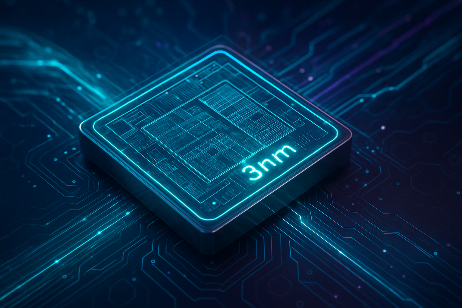
    The Technical Core: Unpacking the Next-Gen Semiconductor Innovations

    The semiconductor industry is undergoing a profound transformation driven by the escalating demands for higher performance, greater energy efficiency, and miniaturization beyond the limits of traditional silicon-based architectures. Emerging semiconductor technologies, encompassing novel materials, advanced transistor designs, and innovative packaging techniques, are poised to reshape the tech industry, particularly in the realm of artificial intelligence (AI).

    Wide-Bandgap Materials: Gallium Nitride (GaN) and Silicon Carbide (SiC)

    Gallium Nitride (GaN) and Silicon Carbide (SiC) are wide-bandgap (WBG) semiconductors that offer significant advantages over conventional silicon, especially in power electronics and high-frequency applications. Silicon has a bandgap of approximately 1.1 eV, while SiC boasts about 3.3 eV and GaN an even wider 3.4 eV. This larger energy difference allows WBG materials to sustain much higher electric fields before breakdown, handling nearly ten times higher voltages and operating at significantly higher temperatures (typically up to 200°C vs. silicon's 150°C). This improved thermal performance leads to better heat dissipation and allows for simpler, smaller, and lighter packaging. Both GaN and SiC exhibit higher electron mobility and saturation velocity, enabling switching frequencies up to 10 times higher than silicon, resulting in lower conduction and switching losses and efficiency improvements of up to 70%.

    While both offer significant improvements, GaN and SiC serve different power applications. SiC devices typically withstand higher voltages (1200V and above) and higher current-carrying capabilities, making them ideal for high-power applications such as automotive and locomotive traction inverters, large solar farms, and three-phase grid converters. GaN excels in high-frequency applications and lower power levels (up to a few kilowatts), offering superior switching speeds and lower losses, suitable for DC-DC converters and voltage regulators in consumer electronics and advanced computing.

    2D Materials: Graphene and Molybdenum Disulfide (MoS₂)

    Two-dimensional (2D) materials, only a few atoms thick, present unique properties for next-generation electronics. Graphene, a semimetal with a zero-electron bandgap, exhibits exceptional electrical and thermal conductivity, mechanical strength, flexibility, and optical transparency. Its high conductivity makes it promising for transparent conductive oxides and interconnects. However, its zero bandgap restricts its direct application in optoelectronics and field-effect transistors where a clear on/off switching characteristic is required.

    Molybdenum Disulfide (MoS₂), a transition metal dichalcogenide (TMDC), has a direct bandgap of 1.8 eV in its monolayer form. Unlike graphene, MoS₂'s natural bandgap makes it highly suitable for applications requiring efficient light absorption and emission, such as photodetectors, LEDs, and solar cells. MoS₂ monolayers have shown strong performance in 5nm electronic devices, including 2D MoS₂-based field-effect transistors and highly efficient photodetectors. Integrating MoS₂ and graphene creates hybrid systems that leverage the strengths of both, for instance, in high-efficiency solar cells or as ohmic contacts for MoS₂ transistors.

    Advanced Architectures: Gate-All-Around FETs (GAA-FETs) and Complementary FETs (CFETs)

    As traditional planar transistors reached their scaling limits, FinFETs emerged as 3D structures. FinFETs utilize a fin-shaped channel surrounded by the gate on three sides, offering improved electrostatic control and reduced leakage. However, at 3nm and below, FinFETs face challenges due to increasing variability and limitations in scaling metal pitch.

    Gate-All-Around FETs (GAA-FETs) overcome these limitations by having the gate fully enclose the entire channel on all four sides, providing superior electrostatic control and significantly reducing leakage and short-channel effects. GAA-FETs, typically constructed using stacked nanosheets, allow for a vertical form factor and continuous variation of channel width, offering greater design flexibility and improved drive current. They are emerging at 3nm and are expected to be dominant at 2nm and below.

    Complementary FETs (CFETs) are a potential future evolution beyond GAA-FETs, expected beyond 2030. CFETs dramatically reduce the footprint area by vertically stacking n-type MOSFET (nMOS) and p-type MOSFET (pMOS) transistors, allowing for much higher transistor density and promising significant improvements in power, performance, and area (PPA).

    Advanced Packaging: Chiplets, 3D Stacking, and Silicon Photonics

    Advanced packaging techniques are critical for continuing performance scaling as Moore's Law slows down, enabling heterogeneous integration and specialized functionalities, especially for AI workloads.

    Chiplets are small, specialized dies manufactured using optimal process nodes for their specific function. Multiple chiplets are assembled into a multi-chiplet module (MCM) or System-in-Package (SiP). This modular approach significantly improves manufacturing yields, allows for heterogeneous integration, and can lead to 30-40% lower energy consumption. It also optimizes cost by using cutting-edge nodes only where necessary.

    3D stacking involves vertically integrating multiple semiconductor dies or wafers using Through-Silicon Vias (TSVs) for vertical electrical connections. This dramatically shortens interconnect distances. 2.5D packaging places components side-by-side on an interposer, increasing bandwidth and reducing latency. True 3D packaging stacks active dies vertically using hybrid bonding, achieving even greater integration density, higher I/O density, reduced signal propagation delays, and significantly lower latency. These solutions can reduce system size by up to 70% and improve overall computing performance by up to 10 times.

    Silicon photonics integrates optical and electronic components on a single silicon chip, using light (photons) instead of electrons for data transmission. This enables extremely high bandwidth and low power consumption. In AI, silicon photonics, particularly through Co-Packaged Optics (CPO), is replacing copper interconnects to reduce power and latency in multi-rack AI clusters and data centers, addressing bandwidth bottlenecks for high-performance AI systems.

    Initial Reactions from the AI Research Community and Industry Experts

    The AI research community and industry experts have shown overwhelmingly positive reactions to these emerging semiconductor technologies. They are recognized as critical for fueling the next wave of AI innovation, especially given AI's increasing demand for computational power, vast memory bandwidth, and ultra-low latency. Experts acknowledge that traditional silicon scaling (Moore's Law) is reaching its physical limits, making advanced packaging techniques like 3D stacking and chiplets crucial solutions. These innovations are expected to profoundly impact various sectors, including autonomous vehicles, IoT, 5G/6G networks, cloud computing, and advanced robotics. Furthermore, AI itself is not only a consumer but also a catalyst for innovation in semiconductor design and manufacturing, with AI algorithms accelerating material discovery, speeding up design cycles, and optimizing power efficiency.

    Corporate Battlegrounds: How Emerging Semiconductors Reshape the Tech Industry

    The rapid evolution of Artificial Intelligence (AI) is heavily reliant on breakthroughs in semiconductor technology. Emerging technologies like wide-bandgap materials, 2D materials, Gate-All-Around FETs (GAA-FETs), Complementary FETs (CFETs), chiplets, 3D stacking, and silicon photonics are reshaping the landscape for AI companies, tech giants, and startups by offering enhanced performance, power efficiency, and new capabilities.

    Wide-Bandgap Materials: Powering the AI Infrastructure

    WBG materials (GaN, SiC) are crucial for power management in energy-intensive AI data centers, allowing for more efficient power delivery to AI accelerators and reducing operational costs. Companies like Nvidia (NASDAQ: NVDA) are already partnering to deploy GaN in 800V HVDC architectures for their next-generation AI processors. Tech giants like Google (NASDAQ: GOOGL), Meta (NASDAQ: META), and AMD (NASDAQ: AMD) will be major consumers for their custom silicon. Navitas Semiconductor (NASDAQ: NVTS) is a key beneficiary, validated as a critical supplier for AI infrastructure through its partnership with Nvidia. Other players like Wolfspeed (NYSE: WOLF), Infineon Technologies (FWB: IFX) (which acquired GaN Systems), ON Semiconductor (NASDAQ: ON), and STMicroelectronics (NYSE: STM) are solidifying their positions. Companies embracing WBG materials will have more energy-efficient and powerful AI systems, displacing silicon in power electronics and RF applications.

    2D Materials: Miniaturization and Novel Architectures

    2D materials (graphene, MoS2) promise extreme miniaturization, enabling ultra-low-power, high-density computing and in-sensor memory for AI. Major foundries like TSMC (NYSE: TSM) and Intel (NASDAQ: INTC) are heavily investing in their research and integration. Startups like Graphenea and Haydale Graphene Industries specialize in producing these nanomaterials. Companies successfully integrating 2D materials for ultra-fast, energy-efficient transistors will gain significant market advantages, although these are a long-term solution to scaling limits.

    Advanced Transistor Architectures: The Core of Future Chips

    GAA-FETs and CFETs are critical for continuing miniaturization and enhancing the performance and power efficiency of AI processors. Foundries like TSMC, Samsung (KRX: 005930), and Intel are at the forefront of developing and implementing these, making their ability to master these nodes a key competitive differentiator. Tech giants designing custom AI chips will leverage these advanced nodes. Startups may face high entry barriers due to R&D costs, but advanced EDA tools from companies like Siemens (FWB: SIE) and Synopsys (NASDAQ: SNPS) will be crucial. Foundries that successfully implement these earliest will attract top AI chip designers.

    Chiplets: Modular Innovation for AI

    Chiplets enable the creation of highly customized, powerful, and energy-efficient AI accelerators by integrating diverse, purpose-built processing units. This modular approach optimizes cost and improves energy efficiency. Tech giants like Google, Amazon (NASDAQ: AMZN), and Microsoft (NASDAQ: MSFT) are heavily reliant on chiplets for their custom AI chips. AMD has been a pioneer, and Intel is heavily invested with its IDM 2.0 strategy. Broadcom (NASDAQ: AVGO) is also developing 3.5D packaging. Chiplets significantly lower the barrier to entry for specialized AI hardware development for startups. This technology fosters an "infrastructure arms race," challenging existing monopolies like Nvidia's dominance.

    3D Stacking: Overcoming the Memory Wall

    3D stacking vertically integrates multiple layers of chips to enhance performance, reduce power, and increase storage capacity. This, especially with High Bandwidth Memory (HBM), is critical for AI accelerators, dramatically increasing bandwidth between processing units and memory. AMD (Instinct MI300 series), Intel (Foveros), Nvidia, Samsung, Micron (NASDAQ: MU), and SK Hynix (KRX: 000660) are heavily investing in this. Foundries like TSMC, Intel, and Samsung are making massive investments in advanced packaging, with TSMC dominating. Companies like Micron are becoming key memory suppliers for AI workloads. This is a foundational enabler for sustaining AI innovation beyond Moore's Law.

    Silicon Photonics: Ultra-Fast, Low-Power Interconnects

    Silicon photonics uses light for data transmission, enabling high-speed, low-power communication. This directly addresses the "bandwidth wall" for real-time AI processing and large language models. Tech giants like Google, Amazon, and Microsoft, invested in cloud AI services, benefit immensely for their data center interconnects. Startups focusing on optical I/O chiplets, like Ayar Labs, are emerging as leaders. Silicon photonics is positioned to solve the "twin crises" of power consumption and bandwidth limitations in AI, transforming the switching layer in AI networks.

    Overall Competitive Implications and Disruption

    The competitive landscape is being reshaped by an "infrastructure arms race" driven by advanced packaging and chiplet integration, challenging existing monopolies. Tech giants are increasingly designing their own custom AI chips, directly challenging general-purpose GPU providers. A severe talent shortage in semiconductor design and manufacturing is exacerbating competition for specialized talent. The industry is shifting from monolithic to modular chip designs, and the energy efficiency imperative is pushing existing inefficient products towards obsolescence. Foundries (TSMC, Intel Foundry Services, Samsung Foundry) and companies providing EDA tools (Arm (NASDAQ: ARM) for architectures, Siemens, Synopsys, Cadence (NASDAQ: CDNS)) are crucial. Memory innovators like Micron and SK Hynix are critical, and strategic partnerships are vital for accelerating adoption.

    The Broader Canvas: AI's Symbiotic Dance with Advanced Semiconductors

    Emerging semiconductor technologies are fundamentally reshaping the landscape of artificial intelligence, enabling unprecedented computational power, efficiency, and new application possibilities. These advancements are critical for overcoming the physical and economic limitations of traditional silicon-based architectures and fueling the current "AI Supercycle."

    Fitting into the Broader AI Landscape

    The relationship between AI and semiconductors is deeply symbiotic. AI's explosive growth, especially in generative AI and large language models (LLMs), is the primary catalyst driving unprecedented demand for smaller, faster, and more energy-efficient semiconductors. These emerging technologies are the engine powering the next generation of AI, enabling capabilities that would be impossible with traditional silicon. They fit into several key AI trends:

    • Beyond Moore's Law: As traditional transistor scaling slows, these technologies, particularly chiplets and 3D stacking, provide alternative pathways to continued performance gains.

    • Heterogeneous Computing: Combining different processor types with specialized memory and interconnects is crucial for optimizing diverse AI workloads, and emerging semiconductors enable this more effectively.

    • Energy Efficiency: The immense power consumption of AI necessitates hardware innovations that significantly improve energy efficiency, directly addressed by wide-bandbandgap materials and silicon photonics.

    • Memory Wall Breakthroughs: AI workloads are increasingly memory-bound. 3D stacking with HBM is directly addressing the "memory wall" by providing massive bandwidth, critical for LLMs.

    • Edge AI: The demand for real-time AI processing on devices with minimal power consumption drives the need for optimized chips using these advanced materials and packaging techniques.

    • AI for Semiconductors (AI4EDA): AI is not just a consumer but also a powerful tool in the design, manufacturing, and optimization of semiconductors themselves, creating a powerful feedback loop.

    Impacts and Potential Concerns

    Positive Impacts: These innovations deliver unprecedented performance, significantly faster processing, higher data throughput, and lower latency, directly translating to more powerful and capable AI models. They bring enhanced energy efficiency, greater customization and flexibility through chiplets, and miniaturization for widespread AI deployment. They also open new AI frontiers like neuromorphic computing and quantum AI, driving economic growth.

    Potential Concerns: The exorbitant costs of innovation, requiring billions in R&D and state-of-the-art fabrication facilities, create high barriers to entry. Physical and engineering challenges, such as heat dissipation and managing complexity at nanometer scales, remain difficult. Supply chain vulnerability, due to extreme concentration of advanced manufacturing, creates geopolitical risks. Data scarcity for AI in manufacturing, and integration/compatibility issues with new hardware architectures, also pose hurdles. Despite efficiency gains, the sheer scale of AI models means overall electricity consumption for AI is projected to rise dramatically, posing a significant sustainability challenge. Ethical concerns about workforce disruption, privacy, bias, and misuse of AI also become more pressing.

    Comparison to Previous AI Milestones

    The current advancements are ushering in an "AI Supercycle" comparable to previous transformative periods. Unlike past milestones often driven by software on existing hardware, this era is defined by deep co-design between AI algorithms and specialized hardware, representing a more profound shift. The relationship is deeply symbiotic, with AI driving hardware innovation and vice versa. These technologies are directly tackling fundamental physical and architectural bottlenecks (Moore's Law limits, memory wall, power consumption) that previous generations faced. The trend is towards highly specialized AI accelerators, often enabled by chiplets and 3D stacking, leading to unprecedented efficiency. The scale of modern AI is vastly greater, necessitating these innovations. A distinct difference is the emergence of AI being used to accelerate semiconductor development and manufacturing itself.

    The Horizon: Charting the Future of Semiconductor Innovation

    Emerging semiconductor technologies are rapidly advancing to meet the escalating demand for more powerful, energy-efficient, and compact electronic devices. These innovations are critical for driving progress in fields like artificial intelligence (AI), automotive, 5G/6G communication, and high-performance computing (HPC).

    Wide-Bandgap Materials (SiC and GaN)

    Near-Term (1-5 years): Continued optimization of manufacturing processes for SiC and GaN, increasing wafer sizes (e.g., to 200mm SiC wafers), and reducing production costs will enable broader adoption. SiC is expected to gain significant market share in EVs, power electronics, and renewable energy.
    Long-Term (Beyond 5 years): WBG semiconductors, including SiC and GaN, will largely replace traditional silicon in power electronics. Further integration with advanced packaging will maximize performance. Diamond (Dia) is emerging as a future ultrawide bandgap semiconductor.
    Applications: EVs (inverters, motor drives, fast charging), 5G/6G infrastructure, renewable energy systems, data centers, industrial power conversion, aerospace, and consumer electronics (fast chargers).
    Challenges: High production costs, material quality and reliability, lack of standardized norms, and limited production capabilities.
    Expert Predictions: SiC will become indispensable for electrification. The WBG technology market is expected to boom, projected to reach around $24.5 billion by 2034.

    2D Materials

    Near-Term (1-5 years): Continued R&D, with early adopters implementing them in niche applications. Hybrid approaches with silicon or WBG semiconductors might be initial commercialization pathways. Graphene is already used in thermal management.
    Long-Term (Beyond 5 years): 2D materials are expected to become standard components in high-performance and next-generation devices, enabling ultra-dense, energy-efficient transistors at atomic scales and monolithic 3D integration. They are crucial for logic applications.
    Applications: Ultra-fast, energy-efficient chips (graphene as optical-electronic translator), advanced transistors (MoS2, InSe), flexible and wearable electronics, high-performance sensors, neuromorphic computing, thermal management, and quantum photonics.
    Challenges: Scalability of high-quality production, compatible fabrication techniques, material stability (degradation by moisture/oxygen), cost, and integration with silicon.
    Expert Predictions: Crucial for future IT, enabling breakthroughs in device performance. The global 2D materials market is projected to reach $4,000 million by 2031, growing at a CAGR of 25.3%.

    Gate-All-Around FETs (GAA-FETs) and Complementary FETs (CFETs)

    Near-Term (1-5 years): GAA-FETs are critical for shrinking transistors beyond 3nm and 2nm nodes, offering superior electrostatic control and reduced leakage. The industry is transitioning to GAA-FETs.
    Long-Term (Beyond 5 years): Exploration of innovative designs like U-shaped FETs and CFETs as successors. CFETs are expected to offer even greater density and efficiency by vertically stacking n-type and p-type GAA-FETs. Research into alternative materials for channels is also on the horizon.
    Applications: HPC, AI processors, low-power logic systems, mobile devices, and IoT.
    Challenges: Fabrication complexities, heat dissipation, leakage currents, material compatibility, and scalability issues.
    Expert Predictions: GAA-FETs are pivotal for future semiconductor technologies, particularly for low-power logic systems, HPC, and AI domains.

    Chiplets

    Near-Term (1-5 years): Broader adoption beyond high-end CPUs and GPUs. The Universal Chiplet Interconnect Express (UCIe) standard is expected to mature, fostering a robust ecosystem. Advanced packaging (2.5D, 3D hybrid bonding) will become standard for HPC and AI, alongside intensified adoption of HBM4.
    Long-Term (Beyond 5 years): Fully modular semiconductor designs with custom chiplets optimized for specific AI workloads will dominate. Transition from 2.5D to more prevalent 3D heterogeneous computing. Co-packaged optics (CPO) are expected to replace traditional copper interconnects.
    Applications: HPC and AI hardware (specialized accelerators, breaking memory wall), CPUs and GPUs, data centers, autonomous vehicles, networking, edge computing, and smartphones.
    Challenges: Standardization (UCIe addressing this), complex thermal management, robust testing methodologies for multi-vendor ecosystems, design complexity, packaging/interconnect technology, and supply chain coordination.
    Expert Predictions: Chiplets will be found in almost all high-performance computing systems, becoming ubiquitous in AI hardware. The global chiplet market is projected to reach hundreds of billions of dollars.

    3D Stacking

    Near-Term (1-5 years): Rapid growth driven by demand for enhanced performance. TSMC (NYSE: TSM), Samsung, and Intel are leading this trend. Quick move towards glass substrates to replace current 2.5D and 3D packaging between 2026 and 2030.
    Long-Term (Beyond 5 years): Increasingly prevalent for heterogeneous computing, integrating different functional layers directly on a single chip. Further miniaturization and integration with quantum computing and photonics. More cost-effective solutions.
    Applications: HPC and AI (higher memory density, high-performance memory, quantum-optimized logic), mobile devices and wearables, data centers, consumer electronics, and automotive.
    Challenges: High manufacturing complexity, thermal management, yield challenges, high cost, interconnect technology, and supply chain.
    Expert Predictions: Rapid growth in the 3D stacking market, with projections ranging from reaching USD 9.48 billion by 2033 to USD 3.1 billion by 2028.

    Silicon Photonics

    Near-Term (1-5 years): Robust growth driven by AI and datacom transceiver demand. Arrival of 3.2Tbps transceivers by 2026. Innovation will involve monolithic integration using quantum dot lasers.
    Long-Term (Beyond 5 years): Pivotal role in next-generation computing, with applications in high-bandwidth chip-to-chip interconnects, advanced packaging, and co-packaged optics (CPO) replacing copper. Programmable photonics and photonic quantum computers.
    Applications: AI data centers, telecommunications, optical interconnects, quantum computing, LiDAR systems, healthcare sensors, photonic engines, and data storage.
    Challenges: Material limitations (achieving optical gain/lasing in silicon), integration complexity (high-powered lasers), cost management, thermal effects, lack of global standards, and production lead times.
    Expert Predictions: Market projected to grow significantly (44-45% CAGR between 2022-2028/2029). AI is a major driver. Key players will emerge, and China is making strides towards global leadership.

    The AI Supercycle: A Comprehensive Wrap-Up of Semiconductor's New Era

    Emerging semiconductor technologies are rapidly reshaping the landscape of modern computing and artificial intelligence, driving unprecedented innovation and projected market growth to a trillion dollars by the end of the decade. This transformation is marked by advancements across materials, architectures, packaging, and specialized processing units, all converging to meet the escalating demands for faster, more efficient, and intelligent systems.

    Key Takeaways

    The core of this revolution lies in several synergistic advancements: advanced transistor architectures like GAA-FETs and the upcoming CFETs, pushing density and efficiency beyond FinFETs; new materials such as Gallium Nitride (GaN) and Silicon Carbide (SiC), which offer superior power efficiency and thermal performance for demanding applications; and advanced packaging technologies including 2.5D/3D stacking and chiplets, enabling heterogeneous integration and overcoming traditional scaling limits by creating modular, highly customized systems. Crucially, specialized AI hardware—from advanced GPUs to neuromorphic chips—is being developed with these technologies to handle complex AI workloads. Furthermore, quantum computing, though nascent, leverages semiconductor breakthroughs to explore entirely new computational paradigms. The Universal Chiplet Interconnect Express (UCIe) standard is rapidly maturing to foster interoperability in the chiplet ecosystem, and High Bandwidth Memory (HBM) is becoming the "scarce currency of AI," with HBM4 pushing the boundaries of data transfer speeds.

    Significance in AI History

    Semiconductors have always been the bedrock of technological progress. In the context of AI, these emerging technologies mark a pivotal moment, driving an "AI Supercycle." They are not just enabling incremental gains but are fundamentally accelerating AI capabilities, pushing beyond the limits of Moore's Law through innovative architectural and packaging solutions. This era is characterized by a deep hardware-software symbiosis, where AI's immense computational demands directly fuel semiconductor innovation, and in turn, these hardware advancements unlock new AI models and applications. This also facilitates the democratization of AI, allowing complex models to run on smaller, more accessible edge devices. The intertwining evolution is so profound that AI is now being used to optimize semiconductor design and manufacturing itself.

    Long-Term Impact

    The long-term impact of these emerging semiconductor technologies will be transformative, leading to ubiquitous AI seamlessly integrated into every facet of life, from smart cities to personalized healthcare. A strong focus on energy efficiency and sustainability will intensify, driven by materials like GaN and SiC and eco-friendly production methods. Geopolitical factors will continue to reshape global supply chains, fostering more resilient and regionally focused manufacturing. New frontiers in computing, particularly quantum AI, promise to tackle currently intractable problems. Finally, enhanced customization and functionality through advanced packaging will broaden the scope of electronic devices across various industrial applications. The transition to glass substrates for advanced packaging between 2026 and 2030 is also a significant long-term shift to watch.

    What to Watch For in the Coming Weeks and Months

    The semiconductor landscape remains highly dynamic. Key areas to monitor include:

    • Manufacturing Process Node Updates: Keep a close eye on progress in the 2nm race and Angstrom-class (1.6nm, 1.8nm) technologies from leading foundries like TSMC (NYSE: TSM) and Intel (NASDAQ: INTC), focusing on their High Volume Manufacturing (HVM) timelines and architectural innovations like backside power delivery.
    • Advanced Packaging Capacity Expansion: Observe the aggressive expansion of advanced packaging solutions, such as TSMC's CoWoS and other 3D IC technologies, which are crucial for next-generation AI accelerators.
    • HBM Developments: High Bandwidth Memory remains critical. Watch for updates on new HBM generations (e.g., HBM4), customization efforts, and its increasing share of the DRAM market, with revenue projected to double in 2025.
    • AI PC and GenAI Smartphone Rollouts: The proliferation of AI-capable PCs and GenAI smartphones, driven by initiatives like Microsoft's (NASDAQ: MSFT) Copilot+ baseline, represents a substantial market shift for edge AI processors.
    • Government Incentives and Supply Chain Shifts: Monitor the impact of government incentives like the US CHIPS and Science Act, as investments in domestic manufacturing are expected to become more evident from 2025, reshaping global supply chains.
    • Neuromorphic Computing Progress: Look for breakthroughs and increased investment in neuromorphic chips that mimic brain-like functions, promising more energy-efficient and adaptive AI at the edge.

    The industry's ability to navigate the complexities of miniaturization, thermal management, power consumption, and geopolitical influences will determine the pace and direction of future innovations.


    This content is intended for informational purposes only and represents analysis of current AI developments.

    TokenRing AI delivers enterprise-grade solutions for multi-agent AI workflow orchestration, AI-powered development tools, and seamless remote collaboration platforms. For more information, visit https://www.tokenring.ai/.

  • Advanced Packaging Market Soars Towards $119.4 Billion by 2032, Igniting a New Era in Semiconductor Innovation

    Advanced Packaging Market Soars Towards $119.4 Billion by 2032, Igniting a New Era in Semiconductor Innovation

    The global Advanced Packaging Market is poised for an explosive growth trajectory, with estimations projecting it to reach an astounding $119.4 billion by 2032. This monumental valuation, a significant leap from an estimated $48.5 billion in 2023, underscores a profound transformation within the semiconductor industry. Far from being a mere protective casing, advanced packaging has emerged as a critical enabler of device performance, efficiency, and miniaturization, fundamentally reshaping how chips are designed, manufactured, and utilized in an increasingly connected and intelligent world.

    This rapid expansion, driven by a Compound Annual Growth Rate (CAGR) of 10.6% from 2024 to 2032, signifies a pivotal shift in the semiconductor value chain. It highlights the indispensable role of sophisticated assembly and interconnection technologies in powering next-generation innovations across diverse sectors. From the relentless demand for smaller, more powerful consumer electronics to the intricate requirements of Artificial Intelligence (AI), 5G, High-Performance Computing (HPC), and the Internet of Things (IoT), advanced packaging is no longer an afterthought but a foundational technology dictating the pace and possibilities of modern technological progress.

    The Engineering Marvels Beneath the Surface: Unpacking Technical Advancements

    The projected surge in the Advanced Packaging Market is intrinsically linked to a wave of groundbreaking technical innovations that are pushing the boundaries of semiconductor integration. These advancements move beyond traditional planar chip designs, enabling a "More than Moore" era where performance gains are achieved not just by shrinking transistors, but by ingeniously stacking and connecting multiple heterogeneous components within a single package.

    Key among these advancements are 2.5D and 3D packaging technologies, which represent a significant departure from conventional approaches. 2.5D packaging, often utilizing silicon interposers with Through-Silicon Vias (TSVs), allows multiple dies (e.g., CPU, GPU, High Bandwidth Memory – HBM) to be placed side-by-side on a single substrate, dramatically reducing the distance between components. This close proximity facilitates significantly faster data transfer rates—up to 35 times faster than traditional motherboards—and enhances overall system performance while improving power efficiency. 3D packaging takes this a step further by stacking dies vertically, interconnected by TSVs, creating ultra-compact, high-density modules. This vertical integration is crucial for applications demanding extreme miniaturization and high computational density, such as advanced AI accelerators and mobile processors.

    Other pivotal innovations include Fan-Out Wafer-Level Packaging (FOWLP) and Fan-Out Panel-Level Packaging (FOPLP). Unlike traditional packaging where the chip is encapsulated within a smaller substrate, FOWLP expands the packaging area beyond the die's dimensions, allowing for more I/O connections and better thermal management. This enables the integration of multiple dies or passive components within a single, thin package without the need for an interposer, leading to cost-effective, high-performance, and miniaturized solutions. FOPLP extends this concept to larger panels, promising even greater cost efficiencies and throughput. These techniques differ significantly from older wire-bonding and flip-chip methods by offering superior electrical performance, reduced form factors, and enhanced thermal dissipation, addressing critical bottlenecks in previous generations of semiconductor assembly. Initial reactions from the AI research community and industry experts highlight these packaging innovations as essential for overcoming the physical limitations of Moore's Law, enabling the complex architectures required for future AI models, and accelerating the deployment of edge AI devices.

    Corporate Chessboard: How Advanced Packaging Reshapes the Tech Landscape

    The burgeoning Advanced Packaging Market is creating a new competitive battleground and strategic imperative for AI companies, tech giants, and startups alike. Companies that master these sophisticated packaging techniques stand to gain significant competitive advantages, influencing market positioning and potentially disrupting existing product lines.

    Leading semiconductor manufacturers and foundries are at the forefront of this shift. Companies like Taiwan Semiconductor Manufacturing Company (TSMC) (NYSE: TSM), Samsung Electronics (KRX: 005930), and Intel Corporation (NASDAQ: INTC) are investing billions in advanced packaging R&D and manufacturing capabilities. TSMC's CoWoS (Chip-on-Wafer-on-Substrate) and InFO (Integrated Fan-Out) technologies, for instance, are critical for packaging high-performance AI chips and GPUs for clients like NVIDIA (NASDAQ: NVDA) and Advanced Micro Devices (NASDAQ: AMD). These investments are not merely about increasing capacity but about developing proprietary intellectual property and processes that differentiate their offerings and secure their role as indispensable partners in the AI supply chain.

    For AI companies and tech giants developing their own custom AI accelerators, such as Google (NASDAQ: GOOGL), Amazon (NASDAQ: AMZN), and Microsoft (NASDAQ: MSFT), access to and expertise in advanced packaging is paramount. It allows them to optimize their hardware for specific AI workloads, achieving unparalleled performance and power efficiency for their data centers and cloud services. Startups focusing on specialized AI hardware also stand to benefit immensely, provided they can leverage these advanced packaging ecosystems to bring their innovative chip designs to fruition. Conversely, companies reliant on older packaging technologies or lacking access to cutting-edge facilities may find themselves at a disadvantage, struggling to meet the performance, power, and form factor demands of next-generation AI applications, potentially leading to disruption of existing products and services. The ability to integrate diverse functionalities—logic, memory, sensors—into a single, compact, and high-performing package is becoming a key differentiator, influencing market share and strategic alliances across the tech industry.

    A New Pillar of the AI Revolution: Broader Significance and Trends

    The ascent of the Advanced Packaging Market to a $119.4 billion valuation by 2032 is not an isolated trend but a fundamental pillar supporting the broader AI landscape and its relentless march towards more powerful and pervasive intelligence. It represents a crucial answer to the increasing computational demands of AI, especially as traditional transistor scaling faces physical and economic limitations.

    This development fits seamlessly into the overarching trend of heterogeneous integration, where optimal performance is achieved by combining specialized processing units rather than relying on a single, monolithic chip. For AI, this means integrating powerful AI accelerators, high-bandwidth memory (HBM), and other specialized silicon into a single, tightly coupled package, minimizing latency and maximizing throughput for complex neural network operations. The impacts are far-reaching: from enabling more sophisticated AI models that demand massive parallel processing to facilitating the deployment of robust AI at the edge, in devices with stringent power and space constraints. Potential concerns, however, include the escalating complexity and cost of these advanced packaging techniques, which could create barriers to entry for smaller players and concentrate manufacturing expertise in a few key regions, raising supply chain resilience questions. This era of advanced packaging stands as a new milestone, comparable in significance to previous breakthroughs in semiconductor fabrication, ensuring that the performance gains necessary for the next wave of AI innovation can continue unabated.

    The Road Ahead: Future Horizons and Looming Challenges

    Looking towards the horizon, the Advanced Packaging Market is set for continuous evolution, driven by the insatiable demands of emerging technologies and the pursuit of even greater integration densities and efficiencies. Experts predict that near-term developments will focus on refining existing 2.5D/3D and fan-out technologies, improving thermal management solutions for increasingly dense packages, and enhancing the reliability and yield of these complex assemblies. The integration of optical interconnects within packages is also on the horizon, promising even faster data transfer rates and lower power consumption, particularly crucial for future data centers and AI supercomputers.

    Long-term developments are expected to push towards even more sophisticated heterogeneous integration, potentially incorporating novel materials and entirely new methods of chip-to-chip communication. Potential applications and use cases are vast, ranging from ultra-compact, high-performance AI modules for autonomous vehicles and robotics to highly specialized medical devices and advanced quantum computing components. However, significant challenges remain. These include the standardization of advanced packaging interfaces, the development of robust design tools that can handle the extreme complexity of 3D-stacked dies, and the need for new testing methodologies to ensure the reliability of these multi-chip systems. Furthermore, the escalating costs associated with advanced packaging R&D and manufacturing, along with the increasing geopolitical focus on semiconductor supply chain security, will be critical factors shaping the market's trajectory. Experts predict a continued arms race in packaging innovation, with a strong emphasis on co-design between chip architects and packaging engineers from the earliest stages of product development.

    A New Era of Integration: The Unfolding Future of Semiconductors

    The projected growth of the Advanced Packaging Market to $119.4 billion by 2032 marks a definitive turning point in the semiconductor industry, signifying that packaging is no longer a secondary process but a primary driver of innovation. The key takeaway is clear: as traditional silicon scaling becomes more challenging, advanced packaging offers a vital pathway to continue enhancing chip functionality, performance, and efficiency, directly enabling the next generation of AI and other transformative technologies.

    This development holds immense significance in AI history, providing the essential hardware foundation for increasingly complex and powerful AI models, from large language models to advanced robotics. It underscores a fundamental shift towards modularity and heterogeneous integration, allowing for specialized components to be optimally combined to create systems far more capable than monolithic designs. The long-term impact will be a sustained acceleration in technological progress, making AI more accessible, powerful, and integrated into every facet of our lives. In the coming weeks and months, industry watchers should keenly observe the continued investments from major semiconductor players, the emergence of new packaging materials and techniques, and the strategic partnerships forming to address the design and manufacturing complexities of this new era of integration. The future of AI, quite literally, is being packaged.

    This content is intended for informational purposes only and represents analysis of current AI developments.

    TokenRing AI delivers enterprise-grade solutions for multi-agent AI workflow orchestration, AI-powered development tools, and seamless remote collaboration platforms.
    For more information, visit https://www.tokenring.ai/.

  • Polysilicon’s Ascendant Reign: Fueling the AI Era and Green Revolution

    Polysilicon’s Ascendant Reign: Fueling the AI Era and Green Revolution

    The polysilicon market is experiencing an unprecedented boom, driven by the relentless expansion of the electronics and solar energy industries. This high-purity form of silicon, a fundamental building block for both advanced semiconductors and photovoltaic cells, is not merely a commodity; it is the bedrock upon which the future of artificial intelligence (AI) and the global transition to sustainable energy are being built. With market valuations projected to reach between USD 106.2 billion and USD 155.87 billion by 2030-2034, polysilicon's critical role in powering our digital world and decarbonizing our planet has never been more pronounced. Its rapid expansion underscores a pivotal moment where technological advancement and environmental imperatives converge, making its supply chain and production innovations central to global progress.

    This surge is predominantly fueled by the insatiable demand for solar panels, which account for a staggering 76% to 91.81% of polysilicon consumption, as nations worldwide push towards aggressive renewable energy targets. Concurrently, the burgeoning electronics sector, propelled by the proliferation of 5G, AI, IoT, and electric vehicles (EVs), continues to drive the need for ultra-high purity polysilicon essential for cutting-edge microchips. The intricate dance between supply, demand, and technological evolution in this market is shaping the competitive landscape for tech giants, influencing geopolitical strategies, and dictating the pace of innovation in critical sectors.

    The Micro-Mechanics of Purity: Siemens vs. FBR and the Quest for Perfection

    The production of polysilicon is a highly specialized and energy-intensive endeavor, primarily dominated by two distinct technologies: the established Siemens process and the emerging Fluidized Bed Reactor (FBR) technology. Each method strives to achieve the ultra-high purity levels required, albeit with different efficiencies and environmental footprints.

    The Siemens process, developed by Siemens AG (FWB: SIE) in 1954, remains the industry's workhorse, particularly for electronics-grade polysilicon. It involves reacting metallurgical-grade silicon with hydrogen chloride to produce trichlorosilane (SiHCl₃), which is then rigorously distilled to achieve exceptional purity (often 9N to 11N, or 99.9999999% to 99.999999999%). This purified gas then undergoes chemical vapor deposition (CVD) onto heated silicon rods, growing them into large polysilicon ingots. While highly effective in achieving stringent purity, the Siemens process is energy-intensive, consuming 100-200 kWh/kg of polysilicon, and operates in batches, making it less efficient than continuous methods. Companies like Wacker Chemie AG (FWB: WCH) and OCI Company Ltd. (KRX: 010060) have continuously refined the Siemens process, improving energy efficiency and yield over decades, proving it to be a "moving target" for alternatives. Wacker, for instance, developed a new ultra-pure grade in 2023 for sub-3nm chip production, with metallic contamination below 5 parts per trillion (ppt).

    Fluidized Bed Reactor (FBR) technology, on the other hand, represents a significant leap towards more sustainable and cost-effective production. In an FBR, silicon seed particles are suspended and agitated by a silicon-containing gas (like silane or trichlorosilane), allowing silicon to deposit continuously onto the particles, forming granules. FBR boasts significantly lower energy consumption (up to 80-90% less electricity than Siemens), a continuous production cycle, and higher output per reactor volume. Companies like GCL Technology Holdings Ltd. (HKG: 3800) and REC Silicon ASA (OSL: RECSI) have made substantial investments in FBR, with GCL-Poly announcing in 2021 that its FBR granular polysilicon achieved monocrystalline purity requirements, potentially outperforming the Siemens process in certain parameters. This breakthrough could drastically reduce the carbon footprint and energy consumption for high-efficiency solar cells. However, FBR still faces challenges such as managing silicon dust (fines), unwanted depositions, and ensuring consistent quality, which historically has limited its widespread adoption for the most demanding electronic-grade applications.

    The distinction between electronics-grade (EG-Si) and solar-grade (SoG-Si) polysilicon is paramount. EG-Si demands ultra-high purity (9N to 11N) to prevent even trace impurities from compromising the performance of sophisticated semiconductor devices. SoG-Si, while still requiring high purity (6N to 9N), has a slightly higher tolerance for certain impurities, balancing cost-effectiveness with solar cell efficiency. The shift towards more efficient solar cell architectures (e.g., N-type TOPCon, heterojunction) is pushing the purity requirements for SoG-Si closer to those of EG-Si, driving further innovation in both production methods. Initial reactions from the industry highlight a dual focus: continued optimization of the Siemens process for the most critical semiconductor applications, and aggressive development of FBR technology to meet the massive, growing demand for solar-grade material with a reduced environmental impact.

    Corporate Chessboard: Polysilicon's Influence on Tech Giants and AI Innovators

    The polysilicon market's dynamics profoundly impact a diverse ecosystem of companies, from raw material producers to chipmakers and renewable energy providers, with significant implications for the AI sector.

    Major Polysilicon Producers are at the forefront. Chinese giants like Tongwei Co., Ltd. (SHA: 600438), GCL Technology Holdings Ltd. (HKG: 3800), Daqo New Energy Corp. (NYSE: DQ), Xinte Energy Co., Ltd. (HKG: 1799), and Asia Silicon (Qinghai) Co., Ltd. dominate the solar-grade market, leveraging cost advantages in raw materials, electricity, and labor. Their rapid capacity expansion has led to China controlling approximately 89% of global solar-grade polysilicon production in 2022. For ultra-high purity electronic-grade polysilicon, companies like Wacker Chemie AG (FWB: WCH), Hemlock Semiconductor Operations LLC (a joint venture involving Dow Inc. (NYSE: DOW) and Corning Inc. (NYSE: GLW)), Tokuyama Corporation (TYO: 4043), and REC Silicon ASA (OSL: RECSI) are critical suppliers, catering to the exacting demands of the semiconductor industry. These firms benefit from premium pricing and long-term contracts for their specialized products.

    The Semiconductor Industry, the backbone of AI, is heavily reliant on a stable supply of high-purity polysilicon. Companies like Intel Corporation (NASDAQ: INTC), Samsung Electronics Co., Ltd. (KRX: 005930), and Taiwan Semiconductor Manufacturing Company Limited (NYSE: TSM) require vast quantities of electronic-grade polysilicon to produce the advanced silicon wafers that become microprocessors, GPUs, and memory chips essential for AI training and inference. Disruptions in polysilicon supply, such as those experienced during the COVID-19 pandemic, can cascade into global chip shortages, directly hindering AI development and deployment. The fact that China, despite its polysilicon dominance, currently lacks the equipment and expertise to produce semiconductor-grade polysilicon at scale creates a strategic vulnerability for non-Chinese chip manufacturers, fostering a push for diversified and localized supply chains, as seen with Hemlock Semiconductor securing a federal grant to expand U.S. production.

    For the Solar Energy Industry, which consumes the lion's share of polysilicon, price volatility and supply chain stability are critical. Solar panel manufacturers, including major players like Longi Green Energy Technology Co., Ltd. (SHA: 601012) and JinkoSolar Holding Co., Ltd. (NYSE: JKS), are directly impacted by polysilicon costs. Recent increases in polysilicon prices, driven by Chinese policy shifts and production cuts, are expected to lead to higher solar module prices, potentially affecting project economics. Companies with vertical integration, from polysilicon production to module assembly, like GCL-Poly, gain a competitive edge by controlling costs and ensuring supply.

    The implications for AI companies, tech giants, and startups are profound. The escalating demand for high-performance AI chips means a continuous and growing need for ultra-high purity electronic-grade polysilicon. This specialized demand, representing a smaller but crucial segment of the overall polysilicon market, could strain existing supply chains. Furthermore, the immense energy consumption of AI data centers (an "unsustainable trajectory") creates a bottleneck in power generation, making access to reliable and affordable energy, increasingly from solar, a strategic imperative. Companies that can secure stable supplies of high-purity polysilicon and leverage energy-efficient technologies (like silicon photonics) will gain a significant competitive advantage. The interplay between polysilicon supply, semiconductor manufacturing, and renewable energy generation directly influences the scalability and sustainability of AI development globally.

    A Foundational Pillar: Polysilicon's Broader Significance in the AI and Green Landscape

    Polysilicon's expanding market transcends mere industrial growth; it is a foundational pillar supporting two of the most transformative trends of our era: the proliferation of artificial intelligence and the global transition to clean energy. Its significance extends to sustainable technology, geopolitical dynamics, and environmental stewardship.

    In the broader AI landscape, polysilicon underpins the very hardware that enables intelligent systems. Every advanced AI model, from large language models to complex neural networks, relies on high-performance silicon-based semiconductors for processing, memory, and high-speed data transfer. The continuous evolution of AI demands increasingly powerful and efficient chips, which in turn necessitates ever-higher purity and quality of electronic-grade polysilicon. Innovations in silicon photonics, allowing light-speed data transmission on silicon chips, are directly tied to polysilicon advancements, promising to address the data transfer bottlenecks that limit AI's scalability and energy efficiency. Thus, the robust health and growth of the polysilicon market are not just relevant; they are critical enablers for the future of AI.

    For sustainable technology, polysilicon is indispensable. It is the core material for photovoltaic solar cells, which are central to decarbonizing global energy grids. As countries commit to aggressive renewable energy targets, the demand for solar panels, and consequently solar-grade polysilicon, will continue to soar. By facilitating the widespread adoption of solar power, polysilicon directly contributes to reducing greenhouse gas emissions and mitigating climate change. Furthermore, advancements in polysilicon recycling from decommissioned solar panels are fostering a more circular economy, reducing waste and the environmental impact of primary production.

    However, this vital material is not without its potential concerns. The most significant is the geopolitical concentration of its supply chain. China's overwhelming dominance in polysilicon production, particularly solar-grade, creates strategic dependencies and vulnerabilities. Allegations of forced labor in the Xinjiang region, a major polysilicon production hub, have led to international sanctions, such as the U.S. Uyghur Forced Labor Prevention Act (UFLPA), disrupting global supply chains and creating a bifurcated market. This geopolitical tension drives efforts by countries like the U.S. to incentivize domestic polysilicon and solar manufacturing to enhance supply chain resilience and reduce reliance on a single, potentially contentious, source.

    Environmental considerations are also paramount. While polysilicon enables clean energy, its production is notoriously energy-intensive, often relying on fossil fuels, leading to a substantial carbon footprint. The Siemens process, in particular, requires significant electricity and can generate toxic byproducts like silicon tetrachloride, necessitating careful management and recycling. The industry is actively pursuing "sustainable polysilicon production" through energy efficiency, waste heat recovery, and the integration of renewable energy sources into manufacturing processes, aiming to lower its environmental impact.

    Comparing polysilicon to other foundational materials, its dual role in both advanced electronics and mainstream renewable energy is unique. While rare-earth elements are vital for specialized magnets and lithium for batteries, silicon, and by extension polysilicon, forms the very substrate of digital intelligence and the primary engine of solar power. Its foundational importance is arguably unmatched, making its market dynamics a bellwether for both technological progress and global sustainability efforts.

    The Horizon Ahead: Navigating Polysilicon's Future

    The polysilicon market stands at a critical juncture, with near-term challenges giving way to long-term growth opportunities, driven by relentless innovation and evolving global priorities. Experts predict a dynamic landscape shaped by technological advancements, new applications, and persistent geopolitical and environmental considerations.

    In the near-term, the market is grappling with significant overcapacity, particularly from China's rapid expansion, which has led to polysilicon prices falling below cash costs for many manufacturers. This oversupply, coupled with seasonal slowdowns in solar installations, is creating inventory build-up. However, this period of adjustment is expected to pave the way for a more balanced market as demand continues its upward trajectory.

    Long-term developments will be characterized by a relentless pursuit of higher purity and efficiency. Fluidized Bed Reactor (FBR) technology is expected to gain further traction, with continuous improvements aimed at reducing manufacturing costs and energy consumption. Breakthroughs like GCL-Poly's (HKG: 3800) FBR granular polysilicon achieving monocrystalline purity requirements signal a shift towards more sustainable and efficient production methods for solar-grade material. For electronics, the demand for ultra-high purity polysilicon (11N or higher) for sub-3nm chip production will intensify, pushing the boundaries of existing Siemens process refinements, as demonstrated by Wacker Chemie AG's (FWB: WCH) recent innovations.

    Polysilicon recycling is also emerging as a crucial future development. As millions of solar panels reach the end of their operational life, closed-loop silicon recycling initiatives will become increasingly vital, offering both environmental benefits and enhancing supply chain resilience. While currently facing economic hurdles, especially for older p-type wafers, advancements in recycling technologies and the growth of n-type and tandem cells are expected to make polysilicon recovery a more viable and significant part of the supply chain by 2035.

    Potential new applications extend beyond traditional solar panels and semiconductors. Polysilicon is finding its way into advanced sensors, Microelectromechanical Systems (MEMS), and critical components for electric and hybrid vehicles. Innovations in thin-film solar cells using polycrystalline silicon are enabling new architectural integrations, such as bent or transparent solar modules, expanding possibilities for green building design and ubiquitous energy harvesting.

    Ongoing challenges include the high energy consumption and associated carbon footprint of polysilicon production, which will continue to drive innovation towards greener manufacturing processes and greater reliance on renewable energy sources for production facilities. Supply chain resilience remains a top concern, with geopolitical tensions and trade restrictions prompting significant investments in domestic polysilicon production in regions like North America and Europe to reduce dependence on concentrated foreign supply. Experts, such as Bernreuter Research, even predict a potential new shortage by 2028 if aggressive capacity elimination continues, underscoring the cyclical nature of this market and the critical need for strategic planning.

    A Future Forged in Silicon: Polysilicon's Enduring Legacy

    The rapid expansion of the polysilicon market is more than a fleeting trend; it is a profound testament to humanity's dual pursuit of advanced technology and a sustainable future. From the intricate circuits powering artificial intelligence to the vast solar farms harnessing the sun's energy, polysilicon is the silent, yet indispensable, enabler.

    The key takeaways are clear: polysilicon is fundamental to both the digital revolution and the green energy transition. Its market growth is driven by unprecedented demand from the semiconductor and solar industries, which are themselves experiencing explosive growth. While the established Siemens process continues to deliver ultra-high purity for cutting-edge electronics, emerging FBR technology promises more energy-efficient and sustainable production for the burgeoning solar sector. The market faces critical challenges, including geopolitical supply chain concentration, energy-intensive production, and price volatility, yet it is responding with continuous innovation in purity, efficiency, and recycling.

    This development's significance in AI history cannot be overstated. Without a stable and increasingly pure supply of polysilicon, the exponential growth of AI, which relies on ever more powerful and energy-efficient chips, would be severely hampered. Similarly, the global push for renewable energy, a critical component of AI's sustainability given its immense data center energy demands, hinges on the availability of affordable, high-quality solar-grade polysilicon. Polysilicon is, in essence, the physical manifestation of the digital and green future.

    Looking ahead, the long-term impact of the polysilicon market's trajectory will be monumental. It will shape the pace of AI innovation, determine the success of global decarbonization efforts, and influence geopolitical power dynamics through control over critical raw material supply chains. The drive for domestic production in Western nations and the continuous technological advancements, particularly in FBR and recycling, will be crucial in mitigating risks and ensuring a resilient supply.

    What to watch for in the coming weeks and months includes the evolution of polysilicon prices, particularly how the current oversupply resolves and whether new shortages emerge as predicted. Keep an eye on new announcements regarding FBR technology breakthroughs and commercial deployments, as these could dramatically shift the cost and environmental footprint of polysilicon production. Furthermore, monitor governmental policies and investments aimed at diversifying supply chains and incentivizing sustainable manufacturing practices outside of China. The story of polysilicon is far from over; it is a narrative of innovation, challenge, and profound impact, continuing to unfold at the very foundation of our technological world.

    This content is intended for informational purposes only and represents analysis of current AI developments.

    TokenRing AI delivers enterprise-grade solutions for multi-agent AI workflow orchestration, AI-powered development tools, and seamless remote collaboration platforms.
    For more information, visit https://www.tokenring.ai/.

  • Chain Reaction Unleashes EL3CTRUM E31: A New Era of Efficiency in Bitcoin Mining Driven by Specialized Semiconductors

    Chain Reaction Unleashes EL3CTRUM E31: A New Era of Efficiency in Bitcoin Mining Driven by Specialized Semiconductors

    The cryptocurrency mining industry is buzzing with the recent announcement from Chain Reaction regarding its EL3CTRUM E31, a new suite of Bitcoin miners poised to redefine the benchmarks for energy efficiency and operational flexibility. This launch, centered around the groundbreaking EL3CTRUM A31 ASIC (Application-Specific Integrated Circuit), signifies a pivotal moment for large-scale mining operations, promising to significantly reduce operational costs and enhance profitability in an increasingly competitive landscape. With its cutting-edge 3nm process node technology, the EL3CTRUM E31 is not just an incremental upgrade but a generational leap, setting new standards for power efficiency and adaptability in the relentless pursuit of Bitcoin.

    The immediate significance of the EL3CTRUM E31 lies in its bold claim of delivering "sub-10 Joules per Terahash (J/TH)" efficiency, a metric that directly translates to lower electricity consumption per unit of computational power. This level of efficiency is critical as the global energy market remains volatile and environmental scrutiny on Bitcoin mining intensifies. Beyond raw power, the EL3CTRUM E31 emphasizes modularity, allowing miners to customize their infrastructure from the chip level up, and integrates advanced features like power curtailment and remote management. These innovations are designed to provide miners with unprecedented control and responsiveness to dynamic power markets, making the EL3CTRUM E31 a frontrunner in the race for sustainable and profitable Bitcoin production.

    Unpacking the Technical Marvel: The EL3CTRUM E31's Core Innovations

    At the heart of Chain Reaction's EL3CTRUM E31 system is the EL3CTRUM A31 ASIC, fabricated using an advanced 3nm process node. This miniaturization of transistor size is the primary driver behind its superior performance and energy efficiency. While samples are anticipated in May 2026 and volume shipments in Q3 2026, the projected specifications are already turning heads.

    The EL3CTRUM E31 is offered in various configurations to suit diverse operational needs and cooling infrastructures:

    • EL3CTRUM E31 Air: Offers a hash rate of 310 TH/s with 3472 W power consumption, achieving an efficiency of 11.2 J/TH.
    • EL3CTRUM E31 Hydro: Designed for liquid cooling, it boasts an impressive 880 TH/s hash rate at 8712 W, delivering a remarkable 9.9 J/TH efficiency.
    • EL3CTRUM E31 Immersion: Provides 396 TH/s at 4356 W, with an efficiency of 11.0 J/TH.

    The specialized ASICs are custom-designed for the SHA-256 algorithm used by Bitcoin, allowing them to perform this specific task with vastly greater efficiency than general-purpose CPUs or GPUs. Chain Reaction's commitment to pushing these boundaries is further evidenced by their active development of 2nm ASICs, promising even greater efficiencies in future iterations. This modular architecture, offering standalone A31 ASIC chips, H31 hashboards, and complete E31 units, empowers miners to optimize their systems for maximum scalability and a lower total cost of ownership. This flexibility stands in stark contrast to previous generations of more rigid, integrated mining units, allowing for tailored solutions based on regional power strategies, climate conditions, and existing facility infrastructure.

    Industry Ripples: Impact on Companies and Competitive Landscape

    The introduction of the EL3CTRUM E31 is set to create significant ripples across the Bitcoin mining industry, benefiting some while presenting formidable challenges to others. Chain Reaction, as the innovator behind this advanced technology, is positioned for substantial growth, leveraging its cutting-edge 3nm ASIC design and a robust supply chain.

    Several key players stand to benefit directly from this development. Core Scientific (NASDAQ: CORZ), a leading North American digital asset infrastructure provider, has a longstanding collaboration with Chain Reaction, recognizing ASIC innovation as crucial for differentiated infrastructure. This partnership allows Core Scientific to integrate EL3CTRUM technology to achieve superior efficiency and scalability. Similarly, ePIC Blockchain Technologies and BIT Mining Limited have also announced collaborations, aiming to deploy next-generation Bitcoin mining systems with industry-leading performance and low power consumption. For large-scale data center operators and industrial miners, the EL3CTRUM E31's efficiency and modularity offer a direct path to reduced operational costs and sustained profitability, especially in dynamic energy markets.

    Conversely, other ASIC manufacturers, such as industry stalwarts Bitmain and Whatsminer, will face intensified competitive pressure. The EL3CTRUM E31's "sub-10 J/TH" efficiency sets a new benchmark, compelling competitors to accelerate their research and development into smaller process nodes and more efficient architectures. Manufacturers relying on older process nodes or less efficient designs risk seeing their market share diminish if they cannot match Chain Reaction's performance metrics. This launch will likely hasten the obsolescence of current and older-generation mining hardware, forcing miners to upgrade more frequently to remain competitive. The emphasis on modular and customizable solutions could also drive a shift in the market, with large operators increasingly opting for components to integrate into custom data center designs, rather than just purchasing complete, off-the-shelf units.

    Wider Significance: Beyond the Mining Farm

    The advancements embodied by the EL3CTRUM E31 extend far beyond the immediate confines of Bitcoin mining, signaling broader trends within the technology and semiconductor industries. The relentless pursuit of efficiency and computational power in specialized hardware design mirrors the trajectory of AI, where purpose-built chips are essential for processing massive datasets and complex algorithms. While Bitcoin ASICs are distinct from AI chips, both fields benefit from the cutting-edge semiconductor manufacturing processes (e.g., 3nm, 2nm) that are pushing the limits of performance per watt.

    Intriguingly, there's a growing convergence between these sectors. Bitcoin mining companies, having established significant energy infrastructure, are increasingly exploring and even pivoting towards hosting AI and High-Performance Computing (HPC) operations. This synergy is driven by the shared need for substantial power and robust data center facilities. The expertise in managing large-scale digital infrastructure, initially developed for Bitcoin mining, is proving invaluable for the energy-intensive demands of AI, suggesting that advancements in Bitcoin mining hardware can indirectly contribute to the overall expansion of the AI sector.

    However, these advancements also bring wider concerns. While the EL3CTRUM E31's efficiency reduces energy consumption per unit of hash power, the overall energy consumption of the Bitcoin network remains a significant environmental consideration. As mining becomes more profitable, miners are incentivized to deploy more powerful hardware, increasing the total hash rate and, consequently, the network's total energy demand. The rapid technological obsolescence of mining hardware also contributes to a growing e-waste problem. Furthermore, the increasing specialization and cost of ASICs contribute to the centralization of Bitcoin mining, making it harder for individual miners to compete with large farms and potentially raising concerns about the network's decentralized ethos. The semiconductor industry, meanwhile, benefits from the demand but also faces challenges from the volatile crypto market and geopolitical tensions affecting supply chains. This evolution can be compared to historical tech milestones like the shift from general-purpose CPUs to specialized GPUs for graphics, highlighting a continuous trend towards optimized hardware for specific, demanding computational tasks.

    The Road Ahead: Future Developments and Expert Predictions

    The future of Bitcoin mining technology, particularly concerning specialized semiconductors, promises continued rapid evolution. In the near term (1-3 years), the industry will see a sustained push towards even smaller and more efficient ASIC chips. While 3nm ASICs like the EL3CTRUM A31 are just entering the market, the development of 2nm chips is already underway, with TSMC planning manufacturing by 2025 and Chain Reaction targeting a 2nm ASIC release in 2027. These advancements, leveraging innovative technologies like Gate-All-Around Field-Effect Transistors (GAAFETs), are expected to deliver further reductions in energy consumption and increases in processing speed. The entry of major players like Intel into the custom cryptocurrency product group also signals increased competition, which is likely to drive further innovation and potentially stabilize hardware pricing. Enhanced cooling solutions, such as hydro and immersion cooling, will also become increasingly standard to manage the heat generated by these powerful chips.

    Longer term (beyond 3 years), while the pursuit of miniaturization will continue, the fundamental economics of Bitcoin mining will undergo a significant shift. With the final Bitcoin projected to be mined around 2140, miners will eventually rely solely on transaction fees for revenue. This necessitates a robust fee market to incentivize miners and maintain network security. Furthermore, AI integration into mining operations is expected to deepen, optimizing power usage, hash rate performance, and overall operational efficiency. Beyond Bitcoin, the underlying technology of advanced ASICs holds potential for broader applications in High-Performance Computing (HPC) and encrypted AI computing, fields where Chain Reaction is already making strides with its "privacy-enhancing processors (3PU)."

    However, significant challenges remain. The ever-increasing network hash rate and difficulty, coupled with Bitcoin halving events (which reduce block rewards), will continue to exert immense pressure on miners to constantly upgrade equipment. High energy costs, environmental concerns, and semiconductor supply chain vulnerabilities exacerbated by geopolitical tensions will also demand innovative solutions and diversified strategies. Experts predict an unrelenting focus on efficiency, a continued geographic redistribution of mining power towards regions with abundant renewable energy and supportive policies, and intensified competition driving further innovation. Bullish forecasts for Bitcoin's price in the coming years suggest continued institutional adoption and market growth, which will sustain the incentive for these technological advancements.

    A Comprehensive Wrap-Up: Redefining the Mining Paradigm

    Chain Reaction's launch of the EL3CTRUM E31 marks a significant milestone in the evolution of Bitcoin mining technology. By leveraging advanced 3nm specialized semiconductors, the company is not merely offering a new product but redefining the paradigm for efficiency, modularity, and operational flexibility in the industry. The "sub-10 J/TH" efficiency target, coupled with customizable configurations and intelligent management features, promises substantial cost reductions and enhanced profitability for large-scale miners.

    This development underscores the critical role of specialized hardware in the cryptocurrency ecosystem and highlights the relentless pace of innovation driven by the demands of Proof-of-Work networks. It sets a new competitive bar for other ASIC manufacturers and will accelerate the obsolescence of less efficient hardware, pushing the entire industry towards more sustainable and technologically advanced solutions. While concerns around energy consumption, centralization, and e-waste persist, the EL3CTRUM E31 also demonstrates how advancements in mining hardware can intersect with and potentially benefit other high-demand computing fields like AI and HPC.

    Looking ahead, the industry will witness a continued "Moore's Law" effect in mining, with 2nm and even smaller chips on the horizon, alongside a growing emphasis on renewable energy integration and AI-driven operational optimization. The strategic partnerships forged by Chain Reaction with industry leaders like Core Scientific signal a collaborative approach to innovation that will be vital in navigating the challenges of increasing network difficulty and fluctuating market conditions. The EL3CTRUM E31 is more than just a miner; it's a testament to the ongoing technological arms race that defines the digital frontier, and its long-term impact will be keenly watched by tech journalists, industry analysts, and cryptocurrency enthusiasts alike in the weeks and months to come.

    This content is intended for informational purposes only and represents analysis of current AI developments.

    TokenRing AI delivers enterprise-grade solutions for multi-agent AI workflow orchestration, AI-powered development tools, and seamless remote collaboration platforms.
    For more information, visit https://www.tokenring.ai/.