Tag: Semiconductors

  • Neuromorphic Dawn: Brain-Inspired Chips Ignite a New Era for AI Hardware

    Neuromorphic Dawn: Brain-Inspired Chips Ignite a New Era for AI Hardware

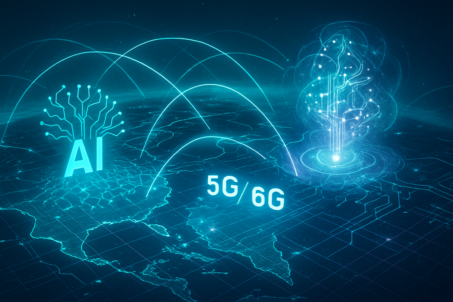
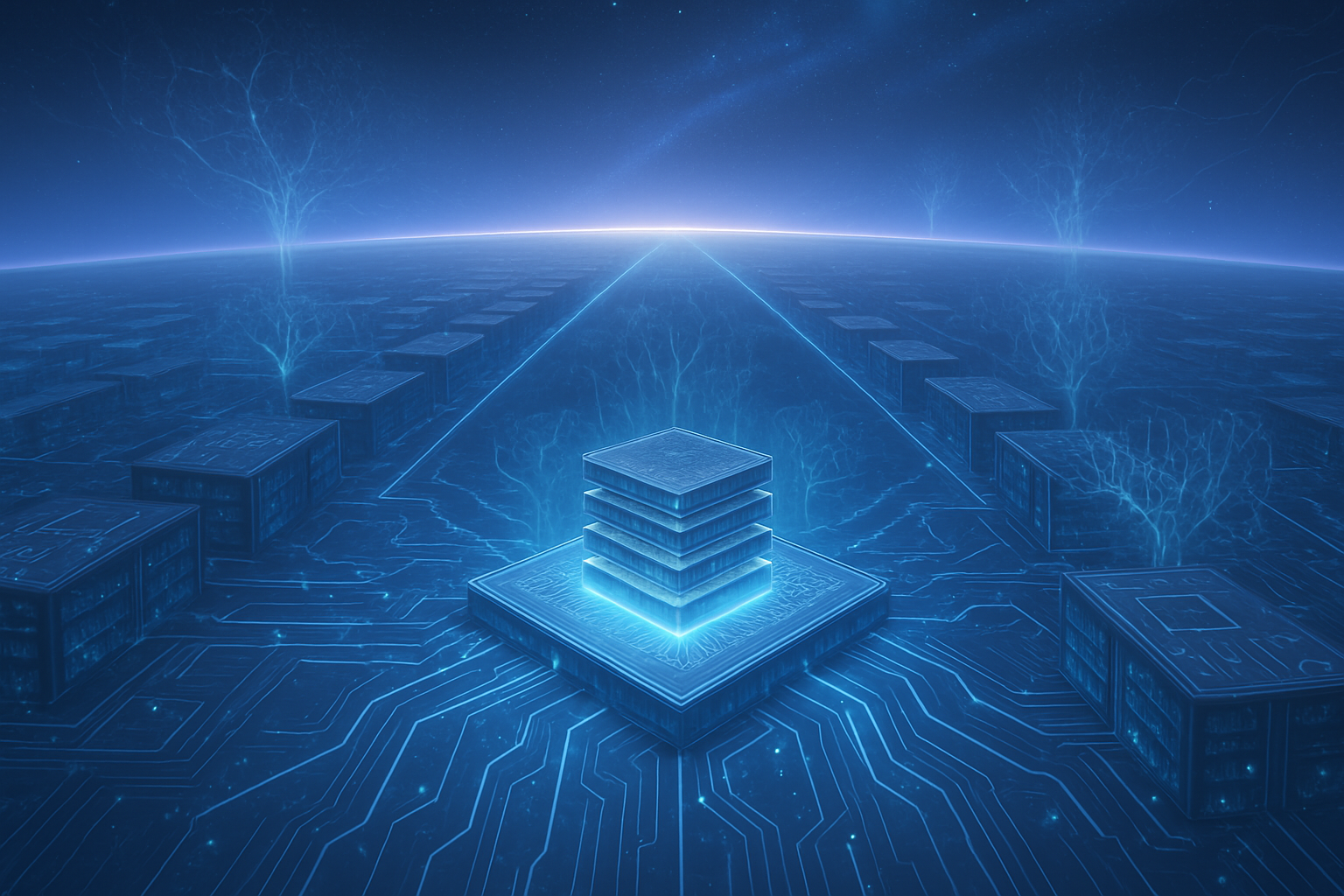
    The artificial intelligence landscape is on the cusp of a profound transformation, driven by unprecedented breakthroughs in neuromorphic computing. As of October 2025, this cutting-edge field, which seeks to mimic the human brain's structure and function, is rapidly transitioning from academic research to commercial viability. These advancements in AI-specific semiconductor architectures promise to redefine computational efficiency, real-time processing, and adaptability for AI workloads, addressing the escalating energy demands and performance bottlenecks of conventional computing.

    The immediate significance of this shift is nothing short of revolutionary. Neuromorphic systems offer radical energy efficiency, often orders of magnitude greater than traditional CPUs and GPUs, making powerful AI accessible in power-constrained environments like edge devices, IoT sensors, and mobile applications. This paradigm shift not only enables more sustainable AI but also unlocks possibilities for real-time inference, on-device learning, and enhanced autonomy, paving the way for a new generation of intelligent systems that are faster, smarter, and significantly more power-efficient.

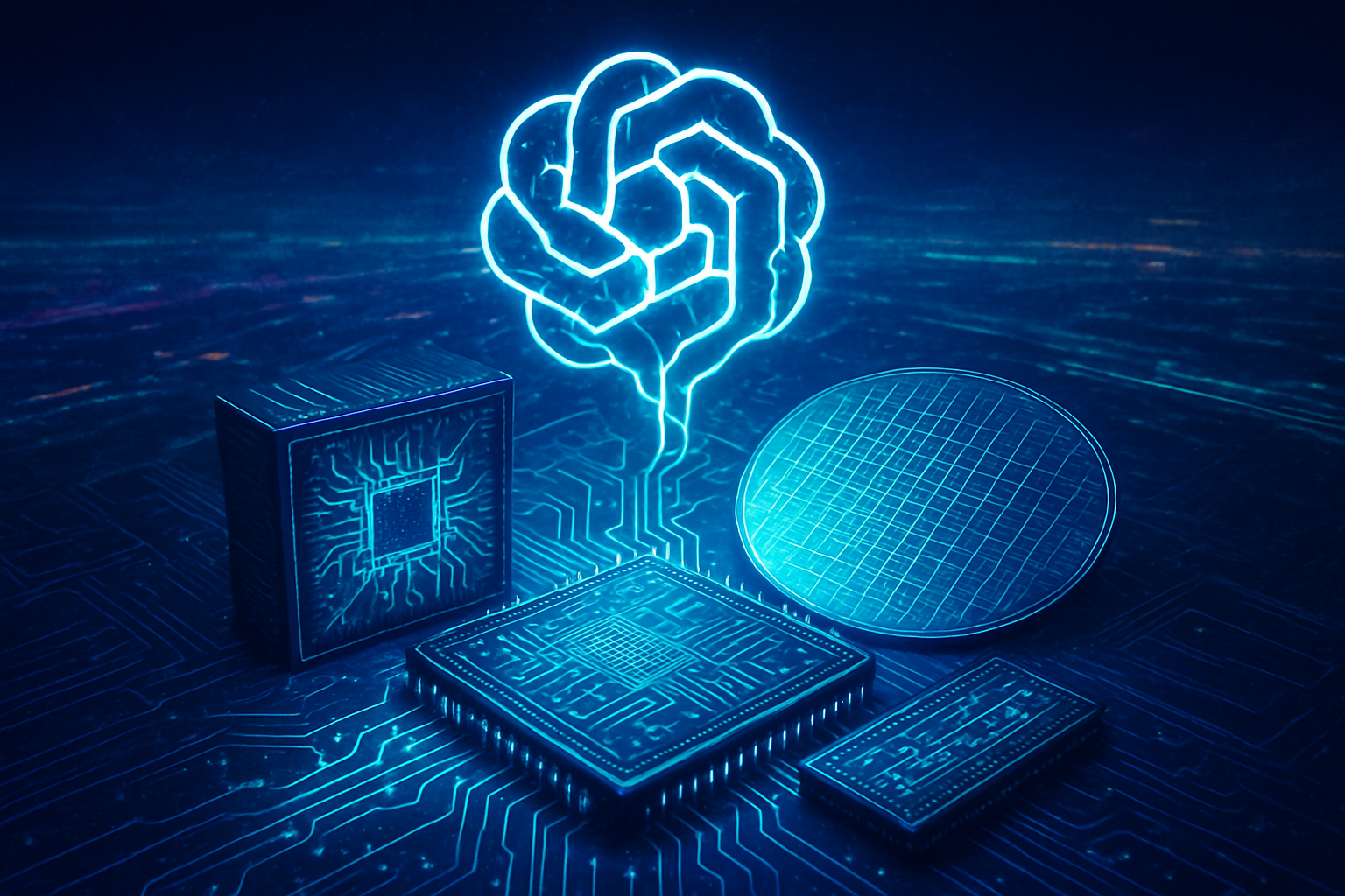
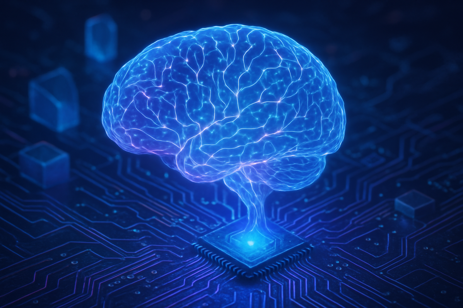
    Technical Marvels: Inside the Brain-Inspired Revolution

    The current wave of neuromorphic innovation is characterized by the deployment of large-scale systems and the commercialization of specialized chips. Intel (NASDAQ: INTC) stands at the forefront with its Hala Point, the largest neuromorphic system to date, housing 1,152 Loihi 2 processors. Deployed at Sandia National Laboratories, this behemoth boasts 1.15 billion neurons and 128 billion synapses across 140,544 neuromorphic processing cores. It delivers state-of-the-art computational efficiencies, achieving over 15 TOPS/W and offering up to 50 times faster processing while consuming 100 times less energy than conventional CPU/GPU systems for certain AI tasks. Intel is further nurturing the ecosystem with its open-source Lava framework.

    Not to be outdone, SpiNNaker 2, a collaboration between SpiNNcloud Systems GmbH, the University of Manchester, and TU Dresden, represents a second-generation brain-inspired supercomputer. TU Dresden has constructed a 5 million core SpiNNaker 2 system, while SpiNNcloud has delivered systems capable of simulating billions of neurons, demonstrating up to 18 times more energy efficiency than current GPUs for AI and high-performance computing (HPC) workloads. Meanwhile, BrainChip (ASX: BRN) is making significant commercial strides with its Akida Pulsar, touted as the world's first mass-market neuromorphic microcontroller for sensor edge applications, boasting 500 times lower energy consumption and 100 times latency reduction compared to conventional AI cores.

    These neuromorphic architectures fundamentally differ from previous approaches by abandoning the traditional von Neumann architecture, which separates memory and processing. Instead, they integrate computation directly into memory, enabling event-driven processing akin to the brain. This "in-memory computing" eliminates the bottleneck of data transfer between processor and memory, drastically reducing latency and power consumption. Companies like IBM (NYSE: IBM) are advancing with their NS16e and NorthPole chips, optimized for neural inference with groundbreaking energy efficiency. Startups like Innatera unveiled their sub-milliwatt, sub-millisecond latency SNP (Spiking Neural Processor) at CES 2025, targeting ambient intelligence, while SynSense offers ultra-low power vision sensors like Speck that mimic biological information processing. Initial reactions from the AI research community are overwhelmingly positive, recognizing 2025 as a "breakthrough year" for neuromorphic computing's transition from academic pursuit to tangible commercial products, backed by significant venture funding.

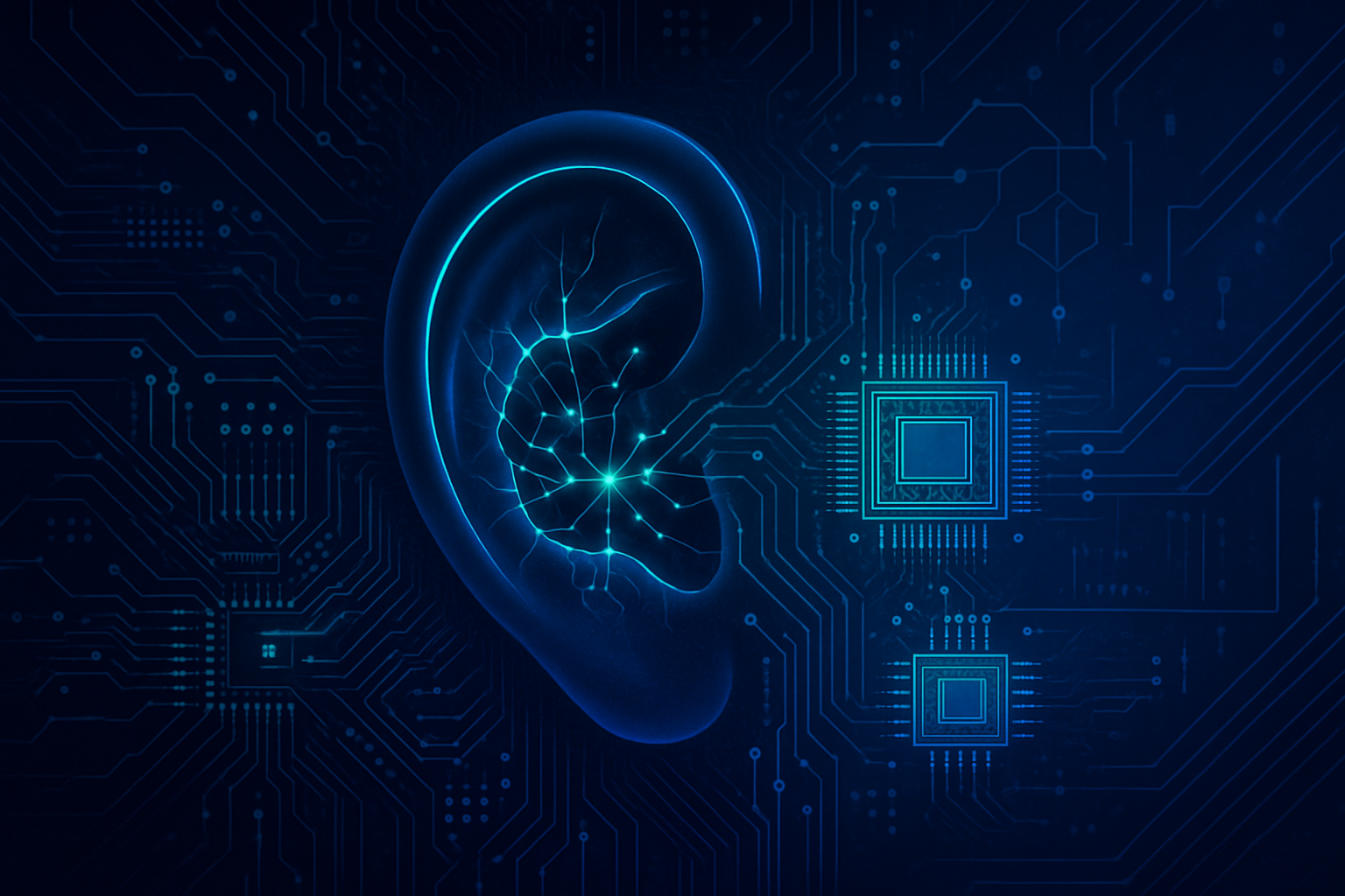
    Event-based sensing, exemplified by Prophesee's Metavision technology, is another critical differentiator. Unlike traditional frame-based vision systems, event-based sensors record only changes in a scene, mirroring human vision. This approach yields exceptionally high temporal resolution, dramatically reduced data bandwidth, and lower power consumption, making it ideal for real-time applications in robotics, autonomous vehicles, and industrial automation. Furthermore, breakthroughs in materials science, such as the discovery that standard CMOS transistors can exhibit neural and synaptic behaviors, and the development of memristive oxides, are crucial for mimicking synaptic plasticity and enabling the energy-efficient in-memory computation that defines this new era of AI hardware.

    Reshaping the AI Industry: A New Competitive Frontier

    The rise of neuromorphic computing promises to profoundly reshape the competitive landscape for AI companies, tech giants, and startups alike. Companies like Intel, IBM, and Samsung (KRX: 005930), with their deep pockets and research capabilities, are well-positioned to leverage their foundational work in chip design and manufacturing to dominate the high-end and enterprise segments. Their large-scale systems and advanced architectures could become the backbone for next-generation AI data centers and supercomputing initiatives.

    However, this field also presents immense opportunities for specialized startups. BrainChip, with its focus on ultra-low power edge AI and on-device learning, is carving out a significant niche in the rapidly expanding IoT and automotive sectors. SpiNNcloud Systems is commercializing large-scale brain-inspired supercomputing, targeting mainstream AI and hybrid models with unparalleled energy efficiency. Prophesee is revolutionizing computer vision with its event-based sensors, creating new markets in industrial automation, robotics, and AR/VR. These agile players can gain significant strategic advantages by specializing in specific applications or hardware configurations, potentially disrupting existing products and services that rely on power-hungry, latency-prone conventional AI hardware.

    The competitive implications extend beyond hardware. As neuromorphic chips enable powerful AI at the edge, there could be a shift away from exclusive reliance on massive cloud-based AI services. This decentralization could empower new business models and services, particularly in industries requiring real-time decision-making, data privacy, and robust security. Companies that can effectively integrate neuromorphic hardware with user-friendly software frameworks, like those being developed by Accenture (NYSE: ACN) and open-source communities, will gain a significant market positioning. The ability to deliver AI solutions with dramatically lower total cost of ownership (TCO) due to reduced energy consumption and infrastructure needs will be a major competitive differentiator.

    Wider Significance: A Sustainable and Ubiquitous AI Future

    The advancements in neuromorphic computing fit perfectly within the broader AI landscape and current trends, particularly the growing emphasis on sustainable AI, decentralized intelligence, and the demand for real-time processing. As AI models become increasingly complex and data-intensive, the energy consumption of training and inference on traditional hardware is becoming unsustainable. Neuromorphic chips offer a compelling solution to this environmental challenge, enabling powerful AI with a significantly reduced carbon footprint. This aligns with global efforts towards greener technology and responsible AI development.

    The impacts of this shift are multifaceted. Economically, neuromorphic computing is poised to unlock new markets and drive innovation across various sectors, from smart cities and autonomous systems to personalized healthcare and industrial IoT. The ability to deploy sophisticated AI capabilities directly on devices reduces reliance on cloud infrastructure, potentially leading to cost savings and improved data security for enterprises. Societally, it promises a future with more pervasive, responsive, and intelligent edge devices that can interact with their environment in real-time, leading to advancements in areas like assistive technologies, smart prosthetics, and safer autonomous vehicles.

    However, potential concerns include the complexity of developing and programming these new architectures, the maturity of the software ecosystem, and the need for standardization across different neuromorphic platforms. Bridging the gap between traditional artificial neural networks (ANNs) and spiking neural networks (SNNs) – the native language of neuromorphic chips – remains a challenge for broader adoption. Compared to previous AI milestones, such as the deep learning revolution which relied on massive parallel processing of GPUs, neuromorphic computing represents a fundamental architectural shift towards efficiency and biological inspiration, potentially ushering in an era where intelligence is not just powerful but also inherently sustainable and ubiquitous.

    The Road Ahead: Anticipating Future Developments

    Looking ahead, the near-term will see continued scaling of neuromorphic systems, with Intel's Loihi platform and SpiNNcloud Systems' SpiNNaker 2 likely reaching even greater neuron and synapse counts. We can expect more commercial products from BrainChip, Innatera, and SynSense to integrate into a wider array of consumer and industrial edge devices. Further advancements in materials science, particularly in memristive technologies and novel transistor designs, will continue to enhance the efficiency and density of neuromorphic chips. The software ecosystem will also mature, with open-source frameworks like Lava, Nengo, and snnTorch gaining broader adoption and becoming more accessible for developers.

    On the horizon, potential applications are vast and transformative. Neuromorphic computing is expected to be a cornerstone for truly autonomous systems, enabling robots and drones to learn and adapt in real-time within dynamic environments. It will power next-generation AR/VR devices with ultra-low latency and power consumption, creating more immersive experiences. In healthcare, it could lead to advanced prosthetics that seamlessly integrate with the nervous system or intelligent medical devices capable of real-time diagnostics and personalized treatments. Ambient intelligence, where environments respond intuitively to human needs, will also be a key beneficiary.

    Challenges that need to be addressed include the development of more sophisticated and standardized programming models for spiking neural networks, making neuromorphic hardware easier to integrate into existing AI pipelines. Cost-effective manufacturing processes for these specialized chips will also be critical for widespread adoption. Experts predict continued significant investment in the sector, with market valuations for neuromorphic-powered edge AI devices projected to reach $8.3 billion by 2030. They anticipate a gradual but steady integration of neuromorphic capabilities into a diverse range of products, initially in specialized domains where energy efficiency and real-time processing are paramount, before broader market penetration.

    Conclusion: A Pivotal Moment for AI

    The breakthroughs in neuromorphic computing mark a pivotal moment in the history of artificial intelligence. We are witnessing the maturation of a technology that moves beyond brute-force computation towards brain-inspired intelligence, offering a compelling solution to the energy and performance demands of modern AI. From large-scale supercomputers like Intel's Hala Point and SpiNNcloud Systems' SpiNNaker 2 to commercial edge chips like BrainChip's Akida Pulsar and IBM's NS16e, the landscape is rich with innovation.

    The significance of this development cannot be overstated. It represents a fundamental shift in how we design and deploy AI, prioritizing sustainability, real-time responsiveness, and on-device intelligence. This will not only enable a new wave of applications in robotics, autonomous systems, and ambient intelligence but also democratize access to powerful AI by reducing its energy footprint and computational overhead. Neuromorphic computing is poised to reshape AI infrastructure, fostering a future where intelligent systems are not only ubiquitous but also environmentally conscious and highly adaptive.

    In the coming weeks and months, industry observers should watch for further product announcements from key players, the expansion of the neuromorphic software ecosystem, and increasing adoption in specialized industrial and consumer applications. The continued collaboration between academia and industry will be crucial in overcoming remaining challenges and fully realizing the immense potential of this brain-inspired revolution.


    This content is intended for informational purposes only and represents analysis of current AI developments.

    TokenRing AI delivers enterprise-grade solutions for multi-agent AI workflow orchestration, AI-powered development tools, and seamless remote collaboration platforms. For more information, visit https://www.tokenring.ai/.

  • US-Taiwan Alliance Forges a New Era in Secure AI, 5G/6G, and Quantum Computing

    US-Taiwan Alliance Forges a New Era in Secure AI, 5G/6G, and Quantum Computing

    The United States and Taiwan are solidifying a strategic technological alliance, marking a pivotal moment in global innovation and geopolitical strategy. This partnership, focusing intently on secure 5G/6G networks, advanced Artificial Intelligence (AI), and groundbreaking Quantum Computing, is designed to enhance supply chain resilience, foster next-generation technological leadership, and counter the influence of authoritarian regimes. This collaboration is particularly significant given Taiwan's indispensable role in advanced semiconductor manufacturing, which underpins much of the world's high-tech industry. The alliance aims to create a robust, democratic technology ecosystem, ensuring that critical future technologies are developed and deployed with shared values of transparency, open competition, and the rule of law.

    Deepening Technical Synergies in Critical Future Tech

    The US-Taiwan collaboration in secure 5G/6G, AI, and Quantum Computing represents a sophisticated technical partnership, moving beyond traditional engagements to prioritize resilient supply chains and advanced research.

    In secure 5G/6G networks, the alliance is championing Open Radio Access Network (Open RAN) architectures to diversify suppliers and reduce reliance on single vendors. Taiwanese hardware manufacturers are crucial in this effort, supplying components for Open RAN deployments globally. Research into 6G technologies is already underway, focusing on AI-native networks, Non-Terrestrial Networks (NTN), Integrated Sensing and Communications (ISAC), and Reconfigurable Intelligent Surfaces (RIS). Taiwan's Industrial Technology Research Institute (ITRI) leads the FORMOSA-6G initiative, encompassing AI-RAN and chip development. A significant push is also seen in Low Earth Orbit (LEO) satellite communications, with Taiwan investing in a "2+4" satellite configuration to enhance communication resilience, particularly against potential disruptions to submarine cables. The Ministry of Digital Affairs (MODA) is encouraging US telecom software and cloud service providers to partner with Taiwanese firms for 5G Private Network Projects. This approach differs from previous ones by explicitly excluding untrusted vendors and focusing on open, interoperable architectures.

    For Artificial Intelligence (AI), the cooperation leverages Taiwan's semiconductor manufacturing prowess and the US's high-performance computing expertise. Key technical areas include Heterogeneous Integration and Advanced Packaging for AI chips, with collaborations between ITRI, the Artificial Intelligence on Chip Taiwan Alliance (AITA), and the UCLA Center for Heterogeneous Integration and Performance Scaling (CHIPS). These efforts are vital for improving die-to-die (D2D) interconnection bandwidth, critical for high-bandwidth applications like 8K imaging and 5G communications. Taiwan's "Taiwan Artificial Intelligence Action Plan 2.0" and "Ten Major AI Infrastructure Projects" aim to establish the island as an AI powerhouse by 2040. Taiwanese companies like Taiwan Semiconductor Manufacturing Company (TSMC) (NYSE: TSM), Foxconn (TWSE: 2317), Quanta (TWSE: 2382), Pegatron (TWSE: 4938), and Wistron (TWSE: 3231) dominate AI server production, and there's a strategic push to shift some AI hardware manufacturing closer to North America to mitigate geopolitical risks. This collaboration ensures Taiwan's unrestricted access to US AI technology, a stark contrast to restrictions faced by other nations.

    In Quantum Computing, the alliance builds on Taiwan's robust semiconductor foundation. Taiwan has already introduced its first five-qubit superconducting quantum computer and researchers at National Tsing Hua University have developed a photonic quantum computer that operates at room temperature, a significant advancement over traditional cryogenic systems. The National Science and Technology Council (NSTC) has established the "National Quantum Team" with a substantial investment to accelerate quantum capabilities, including quantum algorithms and communication. The Taiwan Semiconductor Research Institute (TSRI) is also spearheading a project to fast-track quantum computer subsystem development. US companies like NVIDIA (NASDAQ: NVDA) are forming quantum computing alliances with Taiwanese firms such as Quanta Computing, Compal Electronics (TWSE: 2324), and Supermicro (NASDAQ: SMCI) for hardware testing and optimization. This focus on developing practical, energy-efficient quantum systems, alongside strong international collaboration, aims to position Taiwan as a key player in the global quantum ecosystem.

    Industry Impact: Reshaping Competition and Driving Innovation

    The US-Taiwan tech alliance has profound implications for the global AI and tech industry, creating a landscape of both immense opportunity and heightened competition.

    Taiwan Semiconductor Manufacturing Company (TSMC) (NYSE: TSM) stands as the primary beneficiary. As the world's largest contract chipmaker, its unparalleled advanced manufacturing capabilities (3nm, 2nm, and upcoming 1.6nm processes) are indispensable for AI accelerators, GPUs, and high-performance computing. TSMC's significant investments in the US, including an additional $100 billion in its Arizona operations, aim to bolster the US semiconductor sector while maintaining its core manufacturing strength in Taiwan. This ensures continued access to cutting-edge chip technology for US tech giants.

    Major US tech companies with deep ties to TSMC, such as NVIDIA (NASDAQ: NVDA), Apple (NASDAQ: AAPL), Advanced Micro Devices (AMD) (NASDAQ: AMD), and Qualcomm (NASDAQ: QCOM), are reinforced in their market positions. Their reliance on TSMC for advanced AI accelerators, GPUs, CPUs, and mobile chips is solidified by this alliance, guaranteeing access to leading-edge technology and high yield rates. Google (NASDAQ: GOOGL) also benefits, with its extensive footprint in Taiwan and reliance on TSMC for its AI accelerators. Microsoft (NASDAQ: MSFT) is actively engaging with Taiwanese companies through initiatives like its Azure AI Foundry, fostering co-development, particularly in AI healthcare solutions. Intel (NASDAQ: INTC), through its OpenLab with Quanta Computer Inc. (TWSE: 2382) and strategic investments, is also positioning itself in the 6G and AI PC markets.

    For Taiwanese hardware manufacturers and AI software enablers like ASE Technology Holding Co. Ltd. (NYSE: ASX), MediaTek Inc. (TWSE: 2454), Quanta Computer Inc. (TWSE: 2382), Inventec Corp. (TWSE: 2356), and Delta Electronics, Inc. (TWSE: 2308), the alliance opens doors to increased demand for AI-related technology and strategic collaboration. Taiwan's "IC Taiwan Grand Challenge" in 2025 further aims to foster an IC startup cluster focused on AI chips and high-speed transmission technologies.

    However, the alliance also presents competitive implications and potential disruptions. The emphasis on a "democratic semiconductor supply chain" could lead to technological bipolarity, creating a more fragmented global tech ecosystem. Companies seeking rapid diversification away from Taiwan for advanced chip manufacturing may face higher costs, as US-based manufacturing is estimated to be 30-50% more expensive. Geopolitical risks in the Taiwan Strait remain a significant concern; any disruption could have a devastating impact on the global economy, potentially affecting trillions of dollars in global GDP. Trade conflicts, tariffs, and talent shortages in both the US and Taiwan also pose ongoing challenges. Taiwan's rejection of a "50-50 chip sourcing plan" with the US underscores its intent to protect its "silicon shield" and domestic technological leadership, highlighting potential friction points even within the alliance.

    Broader Implications: Geopolitics, Trends, and the Future of AI

    The US-Taiwan tech alliance for secure 5G/6G, AI, and Quantum Computing extends far beyond bilateral relations, reshaping the broader AI landscape and global geopolitical trends. Taiwan's strategic importance, rooted in its control of over 90% of advanced semiconductor manufacturing (under 7nm), makes it an indispensable player in the global economy and a critical component in the US strategy to counter China's technological rise.

    This alliance profoundly impacts secure 5G/6G. Both nations are committed to developing and deploying networks based on principles of free and fair competition, transparency, and the rule of law. Taiwan's active participation in the US "Clean Network" initiative and its focus on open, interoperable architectures serve as a direct challenge to state-controlled technology models. By strengthening its position in the global 5G supply chain through smart semiconductors and collaborating on resilient infrastructure, Taiwan contributes to a more secure and diversified global telecommunications ecosystem.

    For AI, Taiwan's role is foundational. The alliance ensures a critical supply of high-end chips necessary for training massive AI models and powering edge devices. Companies like NVIDIA (NASDAQ: NVDA) and Google (NASDAQ: GOOGL) are heavily reliant on Taiwan Semiconductor Manufacturing Company (TSMC) (NYSE: TSM) for their AI accelerators. Taiwan's projected control of up to 90% of AI server manufacturing capacity by 2025 underscores its indispensable role in the AI revolution. This partnership fosters a "democratic AI alignment," aiming to develop AI in accordance with democratic values and establishing "trustworthy AI" by ensuring the integrity of data and hardware.

    In Quantum Computing, Taiwan is rapidly emerging as a significant player, building on its semiconductor foundation. Its development of a five-qubit superconducting quantum computer and a room-temperature photonic quantum computer represents major breakthroughs. The substantial investments in the "National Quantum Team" and collaborations with US companies like NVIDIA (NASDAQ: NVDA) aim to accelerate joint research, development, and standardization efforts in this critical field, essential for future secure communications and advanced computation.

    The alliance fits into a broader trend of geopolitical balancing in AI development, where partnerships reflect strategic national interests. Taiwan's "silicon shield" strategy, leveraging its indispensable role in the global tech supply chain, acts as a deterrent against potential aggression. The US CHIPS Act, while aiming to boost domestic production, still relies heavily on Taiwan's expertise, illustrating the complex interdependence. This dynamic contributes to a more regionalized global tech ecosystem, where "trusted technology" based on shared democratic values is prioritized.

    However, potential concerns persist. The concentration of advanced semiconductor manufacturing in Taiwan makes the global supply chain vulnerable to geopolitical instability. The intensified US-China tensions, fueled by this deepened alliance, could increase the risk of conflict. Taiwan's rejection of a "50-50 chip sourcing plan" with the US highlights its determination to protect its technological preeminence and "silicon shield," potentially leading to friction even within the alliance. Furthermore, the economic sovereignty of Taiwan and the potential for rising manufacturing costs due to diversification efforts are ongoing considerations.

    Comparisons to previous AI milestones and technological competitions reveal recurring patterns. Similar to the dot-com boom, AI's economic integration is expanding rapidly. The current race for AI dominance mirrors historical "format wars" (e.g., VHS vs. Betamax), where strategic alliances and ecosystem building are crucial for establishing industry standards. The US-Taiwan alliance is fundamentally about shaping the foundational hardware ecosystem for AI, ensuring it aligns with the interests of democratic nations.

    The Road Ahead: Expected Developments and Emerging Challenges

    The US-Taiwan tech alliance is poised for dynamic evolution, with both near-term and long-term developments shaping the future of secure 5G/6G, AI, and Quantum Computing.

    In the near term (2025-2027), intensified collaboration and strategic investments are expected. The US will continue to encourage Taiwanese semiconductor companies, particularly Taiwan Semiconductor Manufacturing Company (TSMC) (NYSE: TSM), to invest in US manufacturing capacity, building on existing commitments like the $100 billion expansion in Arizona. However, Taiwan will firmly maintain its "silicon shield," prioritizing domestic technological dominance. Taiwan's "AI Action Plan 2.0" and "Ten Major AI Infrastructure Projects" will accelerate AI infrastructure and research, aiming for over $510 billion in economic value by 2040 through initiatives like the Taiwan-Texas AI Innovation Forum and Foxconn's (TWSE: 2317) AI Robotics Industry Grand Alliance. Secure 5G/6G network deployment will deepen, building on the "Clean Network" initiative, with US-based chip designer Qualcomm (NASDAQ: QCOM) joining Taiwan's 5G technology development alliance. Foundational quantum computing initiatives will see Taiwan's "National Quantum Team" progress its $259 million investment, with companies like NVIDIA (NASDAQ: NVDA) forming quantum computing alliances with Taiwanese firms for hardware testing and optimization.

    Looking at long-term developments (beyond 2027), the alliance aims for deeper integration and strategic autonomy. While Taiwan will retain its indispensable role in advanced chip production, the US seeks to significantly increase its domestic chip capacity, potentially reaching 20% globally by the end of the decade, fostering a shared US-Taiwan resilience. Taiwan aspires to become a global AI powerhouse by 2040, focusing on silicon photonics, quantum computing, and AI robotics to establish "Sovereign AI." Both nations will work to lead in 6G and next-generation communication standards, critical for national security and economic prosperity. The advanced quantum ecosystem will see sustained investments in practical quantum computing systems, reliable quantum communication networks, and talent cultivation, with quantum science being a top US R&D priority for 2027.

    Potential applications stemming from this alliance are vast. Secure communications will be enhanced through 5G/6G networks, crucial for critical infrastructure and military operations. Advanced AI capabilities powered by Taiwanese semiconductors will accelerate scientific discovery, nuclear energy research, quantum science, and autonomous systems like drones and robotics. Cybersecurity and national defense will benefit from quantum computing applications and AI integration into defense technologies, providing resilience against future cyberthreats.

    However, challenges persist. Geopolitical tensions in the Taiwan Strait and China's aggressive expansion in semiconductors remain significant risks, potentially impacting the "silicon shield." "America First" policies and potential tariffs on Taiwan-made chips could create friction, although experts advocate for cooperation over tariffs. Balancing supply chain diversification with efficiency, safeguarding Taiwan's technological edge and intellectual property, and addressing growing energy demands for new fabs and AI data centers are ongoing hurdles.

    Expert predictions suggest that technology cooperation and supply chain resilience will remain paramount in US-Taiwan economic relations. The alliance is viewed as critical for maintaining American technological leadership and ensuring Taiwan's security. While the US will boost domestic chip capacity, Taiwan is predicted to retain its indispensable role as the world's epicenter for advanced chip production, vital for the global AI revolution.

    A Strategic Imperative: Concluding Thoughts

    The US-Taiwan alliance for secure 5G/6G, AI, and Quantum Computing represents a monumental strategic pivot in the global technological landscape. At its core, this partnership is a concerted effort to forge a resilient, democratic technology ecosystem, underpinned by Taiwan's unparalleled dominance in advanced semiconductor manufacturing. Key takeaways include the unwavering commitment to "Clean Networks" for 5G/6G, ensuring secure and open telecommunications infrastructure; the deep integration of Taiwan's chip manufacturing prowess with US AI innovation, driving advancements in AI accelerators and servers; and significant joint investments in quantum computing research and development, positioning both nations at the forefront of this transformative field.

    This development holds profound significance in AI history. It marks a decisive move towards "democratic AI alignment," where the development and deployment of critical technologies are guided by shared values of transparency, ethical governance, and human rights, in direct contrast to authoritarian models. The alliance is a proactive strategy for "de-risking" global supply chains, fostering resilience by diversifying manufacturing and R&D within trusted partnerships, rather than a full decoupling. By championing secure networks and hardware integrity, it implicitly defines and promotes "trustworthy AI," setting a precedent for future global standards. Furthermore, it creates interconnected innovation hubs, pooling intellectual capital and manufacturing capabilities to accelerate AI breakthroughs.

    The long-term impact of this alliance is poised to reorder geopolitical dynamics and drive significant economic transformation. It reinforces Taiwan's strategic importance, potentially enhancing its security through its indispensable technological contributions. While fostering a more diversified global technology supply chain, Taiwan is expected to maintain its central role as a high-value R&D and advanced manufacturing hub. This collaboration will accelerate technological advancement in AI, quantum computing, and 6G, setting global standards through joint development of secure protocols and applications. Ultimately, both the US and Taiwan are pursuing "technological sovereignty," aiming to control and develop critical technologies with trusted partners, thereby reducing dependence on potential adversaries.

    In the coming weeks and months, several critical indicators bear watching. The outcomes of future U.S.-Taiwan Economic Prosperity Partnership Dialogues (EPPD) will reveal new initiatives or investment pledges. Progress on tariff negotiations and the implementation of Taiwan's proposed "Taiwan model" for a high-tech strategic partnership, which aims to expand US production without relocating Taiwan's core supply chains, will be crucial. Updates on Taiwan Semiconductor Manufacturing Company's (TSMC) (NYSE: TSM) Arizona fabs and other US CHIPS Act investments will signal the pace of semiconductor supply chain resilience. Developments in Taiwan's AI policy and regulatory frameworks, particularly their alignment with international AI governance principles, will shape the ethical landscape. Finally, milestones from Taiwan's "National Quantum Team" and NVIDIA's (NASDAQ: NVDA) quantum computing alliances, alongside any growing momentum for a broader "T7" alliance of democratic tech powers, will underscore the evolving trajectory of this pivotal technological partnership.

    This content is intended for informational purposes only and represents analysis of current AI developments.

    TokenRing AI delivers enterprise-grade solutions for multi-agent AI workflow orchestration, AI-powered development tools, and seamless remote collaboration platforms.
    For more information, visit https://www.tokenring.ai/.

  • Germany’s €10 Billion Bet: Intel’s Magdeburg Megafab to Anchor European Semiconductor Independence

    Germany’s €10 Billion Bet: Intel’s Magdeburg Megafab to Anchor European Semiconductor Independence

    Berlin, Germany – October 2, 2025 – Over two years ago, on June 19, 2023, a landmark agreement was forged in Berlin, fundamentally reshaping the future of Europe's semiconductor landscape. Intel Corporation (NASDAQ: INTC) officially secured an unprecedented €10 billion (over $10 billion USD at the time of the agreement) in German state subsidies, cementing its commitment to build two state-of-the-art semiconductor manufacturing facilities in Magdeburg. This colossal investment, initially estimated at €30 billion, represented the single largest foreign direct investment in Germany's history and signaled a decisive move by the German government and the European Union to bolster regional semiconductor manufacturing capabilities and reduce reliance on volatile global supply chains.

    The immediate significance of this announcement was profound. For Intel, it solidified a critical pillar in CEO Pat Gelsinger's ambitious "IDM 2.0" strategy, aiming to regain process leadership and expand its global manufacturing footprint. For Germany and the broader European Union, it was a monumental leap towards achieving the goals of the European Chips Act, which seeks to double the EU's share of global chip production to 20% by 2030. This strategic partnership underscored a growing global trend of governments actively incentivizing domestic and regional semiconductor production, driven by geopolitical concerns and the harsh lessons learned from recent chip shortages that crippled industries worldwide.

    A New Era of Advanced Manufacturing: Intel's German Fabs Detailed

    The planned "megafab" complex in Magdeburg is not merely an expansion; it represents a generational leap in European semiconductor manufacturing capabilities. Intel's investment, now projected to exceed €30 billion, will fund two highly advanced fabrication plants (fabs) designed to produce chips utilizing cutting-edge process technologies. These fabs are expected to manufacture chips down to the Angstrom era, including Intel's 20A (equivalent to 2nm class) and 18A (1.8nm class) process nodes, positioning Europe at the forefront of semiconductor innovation. This marks a significant departure from much of Europe's existing, more mature process technology manufacturing, bringing the continent into direct competition with leading-edge foundries in Asia and the United States.

    Technically, these facilities will incorporate extreme ultraviolet (EUV) lithography, a highly complex and expensive technology essential for producing the most advanced chips. The integration of EUV will enable the creation of smaller, more power-efficient, and higher-performing transistors, crucial for next-generation AI accelerators, high-performance computing (HPC), and advanced mobile processors. This differs significantly from older fabrication methods that rely on deep ultraviolet (DUV) lithography, which cannot achieve the same level of precision or transistor density. The initial reactions from the AI research community and industry experts were overwhelmingly positive, viewing the investment as a critical step towards diversifying the global supply of advanced chips, which are increasingly vital for AI development and deployment. The prospect of having a robust, leading-edge foundry ecosystem within Europe is seen as a de-risking strategy against potential geopolitical disruptions and a catalyst for local innovation.

    The Magdeburg fabs are envisioned as a cornerstone of an integrated European semiconductor ecosystem, complementing Intel's existing operations in Ireland (Leixlip) and its planned assembly and test facility in Poland (Wrocław). This multi-site strategy aims to create an end-to-end manufacturing chain within the EU, from wafer fabrication to packaging and testing. The sheer scale and technological ambition of the Magdeburg project are unprecedented for Europe, signaling a strategic intent to move beyond niche manufacturing and become a significant player in the global production of advanced logic chips. This initiative is expected to attract a vast ecosystem of suppliers, research institutions, and skilled talent, further solidifying Europe's position in the global tech landscape.

    Reshaping the AI and Tech Landscape: Competitive Implications and Strategic Advantages

    The establishment of Intel's advanced manufacturing facilities in Germany carries profound implications for AI companies, tech giants, and startups across the globe. Primarily, companies relying on cutting-edge semiconductors for their AI hardware, from training supercomputers to inference engines, stand to benefit immensely. A diversified and geographically resilient supply chain for advanced chips reduces the risks associated with relying on a single region or foundry, potentially leading to more stable pricing, shorter lead times, and greater innovation capacity. This particularly benefits European AI startups and research institutions, granting them closer access to leading-edge process technology.

    The competitive landscape for major AI labs and tech companies will undoubtedly shift. While Intel (NASDAQ: INTC) itself aims to be a leading foundry service provider (Intel Foundry Services), this investment also strengthens its position as a primary supplier of processors and accelerators crucial for AI workloads. Other tech giants like NVIDIA (NASDAQ: NVDA), AMD (NASDAQ: AMD), and even hyperscalers developing their own custom AI silicon could potentially leverage Intel's European fabs for manufacturing, though the primary goal for Intel is to produce its own chips and offer foundry services. The presence of such advanced manufacturing capabilities in Europe could spur a new wave of hardware innovation, as proximity to fabs often fosters closer collaboration between chip designers and manufacturers.

    Potential disruption to existing products or services could arise from increased competition and the availability of more diverse manufacturing options. Companies currently tied to specific foundries might explore new partnerships, leading to a more dynamic and competitive market for chip manufacturing services. Furthermore, the strategic advantage for Intel is clear: by establishing a significant manufacturing presence in Europe, it aligns with governmental incentives, diversifies its global footprint, and positions itself as a critical enabler of European technological sovereignty. This move enhances its market positioning, not just as a chip designer, but as a foundational partner in the continent's digital future, potentially attracting more design wins and long-term contracts from European and international clients.

    Wider Significance: A Cornerstone of European Tech Sovereignty

    Intel's Magdeburg megafab, buoyed by over €10 billion in German subsidies, represents far more than just a factory; it is a cornerstone in Europe's ambitious quest for technological sovereignty and a critical component of the broader global recalibration of semiconductor supply chains. This initiative fits squarely into the overarching trend of "reshoring" or "friend-shoring" critical manufacturing capabilities, a movement accelerated by the COVID-19 pandemic and escalating geopolitical tensions. It signifies a collective recognition that an over-reliance on a geographically concentrated semiconductor industry, particularly in East Asia, poses significant economic and national security risks.

    The impacts of this investment are multifaceted. Economically, it promises thousands of high-tech jobs, stimulates local economies, and attracts a vast ecosystem of ancillary industries and research. Strategically, it provides Europe with a much-needed degree of independence in producing the advanced chips essential for everything from defense systems and critical infrastructure to next-generation AI and automotive technology. This directly addresses the vulnerabilities exposed during the recent global chip shortages, which severely impacted European industries, most notably the automotive sector. The initiative is a direct manifestation of the European Chips Act, a legislative package designed to mobilize over €43 billion in public and private investment to boost the EU's chip-making capacity.

    While the benefits are substantial, potential concerns include the immense scale of the subsidies, raising questions about market distortion and the long-term sustainability of such state aid. There are also challenges related to securing a highly skilled workforce and navigating the complex regulatory environment. Nevertheless, comparisons to previous AI and tech milestones highlight the significance. Just as the development of the internet or the rise of cloud computing fundamentally reshaped industries, the establishment of robust, regional advanced semiconductor manufacturing is a foundational step that underpins all future technological progress, especially in AI. It ensures that Europe will not merely be a consumer of advanced technology but a producer, capable of shaping its own digital destiny.

    The Road Ahead: Anticipated Developments and Lingering Challenges

    The journey for Intel's Magdeburg megafab is still unfolding, with significant developments expected in the near-term and long-term. In the immediate future, focus will remain on the construction phase, with thousands of construction jobs already underway and the complex process of installing highly specialized equipment. We can expect regular updates on construction milestones and potential adjustments to timelines, given the sheer scale and technical complexity of the project. Furthermore, as the facilities near operational readiness, there will be an intensified push for workforce development and training, collaborating with local universities and vocational schools to cultivate the necessary talent pool.

    Longer-term developments include the eventual ramp-up of production, likely commencing in 2027 or 2028, initially focusing on Intel's own leading-edge processors and eventually expanding to offer foundry services to external clients. The potential applications and use cases on the horizon are vast, ranging from powering advanced AI research and supercomputing clusters to enabling autonomous vehicles, sophisticated industrial automation, and cutting-edge consumer electronics. The presence of such advanced manufacturing capabilities within Europe could also foster a boom in local hardware startups, providing them with unprecedented access to advanced fabrication.

    However, significant challenges need to be addressed. Securing a continuous supply of skilled engineers, technicians, and researchers will be paramount. The global competition for semiconductor talent is fierce, and Germany will need robust strategies to attract and retain top-tier professionals. Furthermore, the operational costs of running such advanced facilities are enormous, and maintaining competitiveness against established Asian foundries will require ongoing innovation and efficiency. Experts predict that while the initial investment is a game-changer, the long-term success will hinge on the sustained commitment from both Intel and the German government, as well as the ability to adapt to rapidly evolving technological landscapes. The interplay of geopolitical factors, global economic conditions, and further technological breakthroughs will also shape the trajectory of this monumental undertaking.

    A New Dawn for European Tech: Securing the Future of AI

    Intel's strategic investment in Magdeburg, underpinned by over €10 billion in German subsidies, represents a pivotal moment in the history of European technology and a critical step towards securing the future of AI. The key takeaway is the profound commitment by both a global technology leader and a major European economy to build a resilient, cutting-edge semiconductor ecosystem within the continent. This initiative moves Europe from being primarily a consumer of advanced chips to a significant producer, directly addressing vulnerabilities in global supply chains and fostering greater technological independence.

    This development's significance in AI history cannot be overstated. Advanced semiconductors are the bedrock upon which all AI progress is built. By ensuring a robust, geographically diversified supply of leading-edge chips, Europe is laying the foundation for sustained innovation in AI research, development, and deployment. It mitigates risks associated with geopolitical instability and enhances the continent's capacity to develop and control its own AI hardware infrastructure, a crucial element for national security and economic competitiveness. The long-term impact will likely see a more integrated and self-sufficient European tech industry, capable of driving innovation from silicon to software.

    In the coming weeks and months, all eyes will be on the construction progress in Magdeburg, the ongoing recruitment efforts, and any further announcements regarding partnerships or technological advancements at the site. The success of this megafab will serve as a powerful testament to the effectiveness of government-industry collaboration in addressing strategic technological imperatives. As the world continues its rapid embrace of AI, the ability to manufacture the very components that power this revolution will be a defining factor, and with its Magdeburg investment, Germany and Europe are positioning themselves at the forefront of this new industrial era.

    This content is intended for informational purposes only and represents analysis of current AI developments.

    TokenRing AI delivers enterprise-grade solutions for multi-agent AI workflow orchestration, AI-powered development tools, and seamless remote collaboration platforms.
    For more information, visit https://www.tokenring.ai/.

  • KOSPI Soars Past 3,500 Milestone as Samsung and SK Hynix Power OpenAI’s Ambitious ‘Stargate’ Initiative

    KOSPI Soars Past 3,500 Milestone as Samsung and SK Hynix Power OpenAI’s Ambitious ‘Stargate’ Initiative

    Seoul, South Korea – October 2, 2025 – The Korea Composite Stock Price Index (KOSPI) achieved a historic milestone today, surging past the 3,500-point barrier for the first time ever, closing at an unprecedented 3,549.21. This monumental leap, representing a 2.70% increase on the day and a nearly 48% rise year-to-date, was overwhelmingly fueled by the groundbreaking strategic partnerships between South Korean technology titans Samsung and SK Hynix with artificial intelligence powerhouse OpenAI. The collaboration, central to OpenAI's colossal $500 billion 'Stargate' initiative, has ignited investor confidence, signaling South Korea's pivotal role in the global AI infrastructure race and cementing the critical convergence of advanced semiconductors and artificial intelligence.

    The immediate market reaction was nothing short of euphoric. Foreign investors poured an unprecedented 3.1396 trillion won (approximately $2.3 billion USD) into the South Korean stock market, marking the largest single-day net purchase since 2000. This record influx was a direct response to the heightened expectations for domestic semiconductor stocks, with both Samsung Electronics (KRX: 005930) and SK Hynix (KRX: 000660) experiencing significant share price rallies. SK Hynix shares surged by as much as 12% to an all-time high, while Samsung Electronics climbed up to 5%, reaching a near four-year peak. This collective rally added over $30 billion to their combined market capitalization, propelling the KOSPI to its historic close and underscoring the immense value investors place on securing the hardware backbone for the AI revolution.

    The Technical Backbone of AI's Next Frontier: Stargate and Advanced Memory

    The core of this transformative partnership lies in securing an unprecedented volume of advanced semiconductor solutions, primarily High-Bandwidth Memory (HBM) chips, for OpenAI's 'Stargate' initiative. This colossal undertaking, estimated at $500 billion over the next few years, aims to construct a global network of hyperscale AI data centers to support the development and deployment of next-generation AI models.

    Both Samsung Electronics and SK Hynix have signed letters of intent to supply critical HBM semiconductors, with a particular focus on the latest iterations like HBM3E and the upcoming HBM4. HBM chips are vertically stacked DRAM dies that offer significantly higher bandwidth and lower power consumption compared to traditional DRAM, making them indispensable for powering AI accelerators like GPUs. SK Hynix, a recognized market leader in HBM, is poised to be a key supplier, also collaborating with TSMC (NYSE: TSM) on HBM4 development. Samsung, while aggressively developing HBM4, will also leverage its broader semiconductor portfolio, including logic and foundry services, advanced chip packaging technologies, and heterogeneous integration, to provide end-to-end solutions for OpenAI. OpenAI's projected memory demand for Stargate is staggering, anticipated to reach up to 900,000 DRAM wafers per month by 2029 – a volume that more than doubles the current global HBM industry capacity and roughly 40% of the total global DRAM output.

    This collaboration signifies a fundamental departure from previous AI infrastructure approaches. Instead of solely relying on general-purpose GPUs and their integrated memory from vendors like Nvidia (NASDAQ: NVDA), OpenAI is moving towards greater vertical integration and direct control over its underlying hardware. This involves securing a direct and stable supply of critical memory components and exploring its own custom AI application-specific integrated circuit (ASIC) chip design. The partnership extends beyond chip supply, encompassing the design, construction, and operation of AI data centers, with Samsung SDS (KRX: 018260) and SK Telecom (KRX: 017670) involved in various aspects, including the exploration of innovative floating data centers by Samsung C&T (KRX: 028260) and Samsung Heavy Industries (KRX: 010140). This holistic, strategic alliance ensures a critical pipeline of memory chips and infrastructure for OpenAI, providing a more optimized and efficient hardware stack for its demanding AI workloads.

    Initial reactions from the AI research community and industry experts have been largely positive, acknowledging the "undeniable innovation and market leadership" demonstrated by OpenAI and its partners. Many see the securing of such massive, dedicated supply lines as absolutely critical for sustaining the rapid pace of AI innovation. However, some analysts have expressed cautious skepticism regarding the sheer scale of the projected memory demand, with some questioning the feasibility of 900,000 wafers per month, and raising concerns about potential speculative bubbles in the AI sector. Nevertheless, the consensus generally leans towards recognizing these partnerships as crucial for the future of AI development.

    Reshaping the AI Landscape: Competitive Implications and Market Shifts

    The Samsung/SK Hynix-OpenAI partnership is set to dramatically reshape the competitive landscape for AI companies, tech giants, and even startups. OpenAI stands as the primary beneficiary, gaining an unparalleled strategic advantage by securing direct access to an immense and stable supply of cutting-edge HBM and DRAM chips. This mitigates significant supply chain risks and is expected to accelerate the development of its next-generation AI models and custom AI accelerators, vital for its pursuit of artificial general intelligence (AGI).

    The Samsung Group and SK Group affiliates are also poised for massive gains. Samsung Electronics and SK Hynix will experience a guaranteed, substantial revenue stream from the burgeoning AI sector, solidifying their leadership in the advanced memory market. Samsung SDS will benefit from providing expertise in AI data center design and operations, while Samsung C&T and Samsung Heavy Industries will lead innovative floating offshore data center development. SK Telecom will collaborate on building AI data centers in Korea, leveraging its telecommunications infrastructure. Furthermore, South Korea itself stands to benefit immensely, positioning itself as a critical hub for global AI infrastructure, attracting significant investment and promoting economic growth.

    For OpenAI's rivals, such as Google DeepMind (NASDAQ: GOOGL), Anthropic, and Meta AI (NASDAQ: META), this partnership intensifies the "AI arms race." OpenAI's secured access to vast HBM volumes could make it harder or more expensive for competitors to acquire necessary high-performance memory chips, potentially creating an uneven playing field. While Nvidia's GPUs remain dominant, OpenAI's move towards custom silicon, supported by these memory alliances, signals a long-term strategy for diversification that could eventually temper Nvidia's near-monopoly. Other tech giants like Google (NASDAQ: GOOGL), Microsoft (NASDAQ: MSFT), and Amazon (NASDAQ: AMZN), already developing their own proprietary AI chips, will face increased pressure to accelerate their custom hardware development efforts to secure their AI compute supply chains. Memory market competitors like Micron Technology (NASDAQ: MU) will find it challenging to expand their market share against the solidified duopoly of Samsung and SK Hynix in the HBM market.

    The immense demand from OpenAI could lead to several disruptions, including potential supply shortages and price increases for HBM and DRAM, disproportionately affecting smaller companies. It will also force memory manufacturers to reconfigure production lines, traditionally tied to cyclical PC and smartphone demand, to prioritize the consistent, high-growth demand from the AI sector. Ultimately, this partnership grants OpenAI greater control over its hardware destiny, reduces reliance on third-party suppliers, and accelerates its ability to innovate. It cements Samsung and SK Hynix's market positioning as indispensable suppliers, transforming the historically cyclical memory business into a more stable growth engine, and reinforces South Korea's ambition to become a global AI hub.

    A New Era: Wider Significance and Geopolitical Currents

    This alliance between OpenAI, Samsung, and SK Hynix marks a profound development within the broader AI landscape, signaling a critical shift towards deeply integrated hardware-software strategies. It highlights a growing trend where leading AI developers are exerting greater control over their fundamental hardware infrastructure, recognizing that software advancements must be paralleled by breakthroughs and guaranteed access to underlying hardware. This aims to mitigate supply chain risks and accelerate the development of next-generation AI models and potentially Artificial General Intelligence (AGI).

    The partnership will fundamentally reshape global technology supply chains, particularly within the memory chip market. OpenAI's projected demand of 900,000 DRAM wafers per month by 2029 could account for as much as 40% of the total global DRAM output, straining and redefining industry capacities. This immense demand from a single entity could lead to price increases or shortages for other industries and create an uneven playing field. Samsung and SK Hynix, with their combined 70% share of the global DRAM market and nearly 80% of the HBM market, are indispensable partners. This collaboration also emphasizes a broader trend of prioritizing supply chain resilience and regionalization, often driven by geopolitical considerations.

    The escalating energy consumption of AI data centers is a major concern, and this partnership seeks to address it through innovative solutions. The exploration of floating offshore data centers by Samsung C&T and Samsung Heavy Industries offers potential benefits such as lower cooling costs, reduced carbon emissions, and a solution to land scarcity. More broadly, memory subsystems can account for up to 50% of the total system power in modern AI clusters, making energy efficiency a strategic imperative as power becomes a limiting factor for scaling AI infrastructure. Innovations like computational random-access memory (CRAM) and in-memory computing (CIM) are being explored to dramatically reduce power demands.

    This partnership significantly bolsters South Korea's national competitiveness in the global AI race, reinforcing its position as a critical global AI hub. For the United States, the alliance with South Korean chipmakers aligns with its strategic interest in securing access to advanced semiconductors crucial for AI leadership. Countries worldwide are investing heavily in domestic chip production and forming strategic alliances, recognizing that technological leadership translates into national security and economic prosperity.

    However, concerns regarding market concentration and geopolitical implications are also rising. The AI memory market is already highly concentrated, and OpenAI's unprecedented demand could further intensify this, potentially leading to price increases or supply shortages for other companies. Geopolitically, this partnership occurs amidst escalating "techno-nationalism" and a "Silicon Curtain" scenario, where advanced semiconductors are strategic assets fueling intense competition between global powers. South Korea's role as a vital supplier to the US-led tech ecosystem is elevated but also complex, navigating these geopolitical tensions.

    While previous AI milestones often focused on algorithmic advancements (like AlphaGo's victory), this alliance represents a foundational shift in how the infrastructure for AI development is approached. It signals a recognition that the physical limitations of hardware, particularly memory, are now a primary bottleneck for achieving increasingly ambitious AI goals, including AGI. It is a strategic move to secure the computational "fuel" for the next generation of AI, indicating that the era of relying solely on incremental improvements in general-purpose hardware is giving way to highly customized and secured supply chains for AI-specific infrastructure.

    The Horizon of AI: Future Developments and Challenges Ahead

    The Samsung/SK Hynix-OpenAI partnership is set to usher in a new era of AI capabilities and infrastructure, with significant near-term and long-term developments on the horizon. In the near term, the immediate focus will be on ramping up the supply of cutting-edge HBM and high-performance DRAM to meet OpenAI's projected demand of 900,000 DRAM wafers per month by 2029. Samsung SDS will actively collaborate on the design and operation of Stargate AI data centers, with SK Telecom exploring a "Stargate Korea" initiative. Samsung SDS will also extend its expertise to provide enterprise AI services and act as an official reseller of OpenAI's services in Korea, facilitating the adoption of ChatGPT Enterprise.

    Looking further ahead, the long-term vision includes the development of next-generation global AI data centers, notably the ambitious joint development of floating data centers by Samsung C&T and Samsung Heavy Industries. These innovative facilities aim to address land scarcity, reduce cooling costs, and lower carbon emissions. Samsung Electronics will also contribute its differentiated capabilities in advanced chip packaging and heterogeneous integration, while both companies intensify efforts to develop and mass-produce next-generation HBM4 products. This holistic innovation across the entire AI stack—from memory semiconductors and data centers to energy solutions and networks—is poised to solidify South Korea's role as a critical global AI hub.

    The enhanced computational power and optimized infrastructure resulting from this partnership are expected to unlock unprecedented AI applications. We can anticipate the training and deployment of even larger, more sophisticated generative AI models, leading to breakthroughs in natural language processing, image generation, video creation, and multimodal AI. This could dramatically accelerate scientific discovery in fields like drug discovery and climate modeling, and lead to more robust autonomous systems. By expanding infrastructure and enterprise services, cutting-edge AI could also become more accessible, fostering innovation across various industries and potentially enabling more powerful and efficient AI processing at the edge.

    However, significant challenges must be addressed. The sheer manufacturing scale required to meet OpenAI's demand, which more than doubles current HBM industry capacity, presents a massive hurdle. The immense energy consumption of hyperscale AI data centers remains a critical environmental and operational challenge, even with innovative solutions like floating data centers. Technical complexities associated with advanced chip packaging, heterogeneous integration, and floating data center deployment are substantial. Geopolitical factors, including international trade policies and export controls, will continue to influence supply chains and resource allocation, particularly as nations pursue "sovereign AI" capabilities. Finally, the estimated $500 billion cost of the Stargate project highlights the immense financial investment required.

    Industry experts view this semiconductor alliance as a "defining moment" for the AI landscape, signifying a critical convergence of AI development and semiconductor manufacturing. They predict a growing trend of vertical integration, with AI developers seeking greater control over their hardware destiny. The partnership is expected to fundamentally reshape the memory chip market for years to come, emphasizing the need for deeper hardware-software co-design. While focused on memory, the long-term collaboration hints at future custom AI chip development beyond general-purpose GPUs, with Samsung's foundry capabilities potentially playing a key role.

    A Defining Moment for AI and Global Tech

    The KOSPI's historic surge past the 3,500-point mark, driven by the Samsung/SK Hynix-OpenAI partnerships, encapsulates a defining moment in the trajectory of artificial intelligence and the global technology industry. It vividly illustrates the unprecedented demand for advanced computing hardware, particularly High-Bandwidth Memory, that is now the indispensable fuel for the AI revolution. South Korean chipmakers have cemented their pivotal role as the enablers of this new era, their technological prowess now intrinsically linked to the future of AI.

    The key takeaways from this development are clear: the AI industry's insatiable demand for HBM is reshaping the semiconductor market, South Korea is emerging as a critical global AI infrastructure hub, and the future of AI development hinges on broad, strategic collaborations that span hardware and software. This alliance is not merely a supplier agreement; it represents a deep, multifaceted partnership aimed at building the foundational infrastructure for artificial general intelligence.

    In the long term, this collaboration promises to accelerate AI development, redefine the memory market from cyclical to consistently growth-driven, and spur innovation in data center infrastructure, including groundbreaking solutions like floating data centers. Its geopolitical implications are also significant, intensifying the global competition for AI leadership and highlighting the strategic importance of controlling advanced semiconductor supply chains. The South Korean economy, heavily reliant on semiconductor exports, stands to benefit immensely, solidifying its position on the global tech stage.

    As the coming weeks and months unfold, several key aspects warrant close observation. We will be watching for the detailed definitive agreements that solidify the letters of intent, including specific supply volumes and financial terms. The progress of SK Hynix and Samsung in rapidly expanding HBM production capacity, particularly Samsung's push in next-generation HBM4, will be crucial. Milestones in the construction and operational phases of OpenAI's Stargate data centers, especially the innovative floating designs, will provide tangible evidence of the partnership's execution. Furthermore, the responses from other memory manufacturers (like Micron Technology) and major AI companies to this significant alliance will indicate how the competitive landscape continues to evolve. Finally, the KOSPI index and the broader performance of related semiconductor and technology stocks will serve as a barometer of market sentiment and the realization of the anticipated growth and impact of this monumental collaboration.

    This content is intended for informational purposes only and represents analysis of current AI developments.

    TokenRing AI delivers enterprise-grade solutions for multi-agent AI workflow orchestration, AI-powered development tools, and seamless remote collaboration platforms.
    For more information, visit https://www.tokenring.ai/.

  • MIJ’s ‘Physical AI’ Breaks Barriers: From Tinnitus Care to Semiconductors and Defense

    MIJ’s ‘Physical AI’ Breaks Barriers: From Tinnitus Care to Semiconductors and Defense

    In a striking display of cross-industry innovation, MIJ Co., Ltd., a pioneering firm initially recognized for its advanced tinnitus care solutions, has announced a significant strategic expansion of its 'Physical AI' Healthcare Platform into the high-stakes sectors of semiconductors and defense. This audacious move, unveiled in 2025, positions MIJ as a unique player at the intersection of medical technology, advanced hardware design, and national security, leveraging its core competencies in real-world AI applications.

    This expansion transcends traditional industry silos, illustrating a burgeoning trend where specialized AI capabilities developed for one domain find powerful new applications in seemingly disparate fields. MIJ's journey from addressing a pervasive health issue like tinnitus to contributing to critical infrastructure and defense capabilities highlights the adaptable and transformative potential of 'Physical AI'—AI systems designed to directly interact with and adapt to the physical environment through tangible hardware solutions.

    The Technical Backbone of Cross-Sector AI Innovation

    At the heart of MIJ's (MIJ Co., Ltd.) 'Physical AI' platform is a sophisticated blend of hardware and software engineering, initially honed through its ETEREOCARE management platform and the ETEREO TC Square headset. This system, designed for tinnitus management, utilizes bone conduction technology at the mastoid to deliver personalized adaptation sounds, minimizing ear fatigue and promoting user adherence. The platform's ability to track hearing data and customize therapies showcases MIJ's foundational expertise in real-time physiological data processing and adaptive AI.

    The technical specifications underpinning MIJ's broader 'Physical AI' ambitions are robust. The company boasts in-house fabless design capabilities, culminating in its proprietary AI Edge Board dubbed "PotatoPi." This edge board signifies a commitment to on-device AI processing, reducing latency and reliance on cloud infrastructure—a critical requirement for real-time applications in defense and medical imaging. Furthermore, MIJ's extensive portfolio of 181 Intellectual Property (IP) cores, encompassing high-speed interfaces, audio/video processing, analog-to-digital (AD) and digital-to-analog (DA) conversion, and various communication protocols, provides a versatile toolkit for developing diverse semiconductor solutions. This broad IP base enables the creation of specialized hardware for medical devices, FPGA (Field-Programmable Gate Array) solutions, and System-on-Chip (SoC) designs. The company's future plans include next-generation AI-driven models for hearing devices, suggesting advanced algorithms for personalized sound adaptation and sophisticated hearing health management. This approach significantly differs from traditional AI, which often operates purely in digital or virtual environments; 'Physical AI' directly bridges the gap between digital intelligence and physical action, enabling machines to perform complex tasks in unpredictable real-world conditions. Initial reactions from the AI research community emphasize the growing importance of edge AI and hardware-software co-design, recognizing MIJ's move as a practical demonstration of these theoretical advancements.

    Reshaping the Competitive Landscape: Implications for AI, Tech, and Startups

    MIJ's strategic pivot carries significant implications for a diverse array of companies across the AI, tech, and defense sectors. MIJ itself stands to benefit immensely by diversifying its revenue streams and expanding its market reach beyond specialized healthcare. Its comprehensive IP core portfolio and fabless design capabilities position it as a formidable contender in the embedded AI and custom semiconductor markets, directly competing with established FPGA and SoC providers.

    For major AI labs and tech giants, MIJ's expansion highlights the increasing value of specialized, real-world AI applications. While large tech companies often focus on broad AI platforms and cloud services, MIJ's success in 'Physical AI' demonstrates the competitive advantage of deeply integrated hardware-software solutions. This could prompt tech giants to either acquire companies with similar niche expertise or accelerate their own development in edge AI and custom silicon. Startups specializing in embedded AI, sensor technology, and custom chip design might find new opportunities for partnerships or face increased competition from MIJ's proven capabilities. The defense sector, typically dominated by large contractors, could see disruption as agile, AI-first companies like MIJ introduce more efficient and intelligent solutions for military communications, surveillance, and operational support. The company's entry into the Defense Venture Center in Korea is a clear signal of its intent to carve out a significant market position.

    Broader Significance: AI's March Towards Tangible Intelligence

    MIJ's cross-industry expansion is a microcosm of a larger, transformative trend in the AI landscape: the shift from purely digital intelligence to 'Physical AI.' This development fits squarely within the broader movement towards edge computing, where AI processing moves closer to the data source, enabling real-time decision-making crucial for autonomous systems, smart infrastructure, and critical applications. It underscores the growing recognition that AI's ultimate value often lies in its ability to interact intelligently with the physical world.

    The impacts are far-reaching. In healthcare, it could accelerate the development of personalized, adaptive medical devices. In semiconductors, it demonstrates the demand for highly specialized, AI-optimized hardware. For the defense sector, it promises more intelligent, responsive, and efficient systems, from advanced communication equipment to sophisticated sensor interfaces. Potential concerns, however, also emerge, particularly regarding the ethical implications of deploying advanced AI in defense applications. The dual-use nature of technologies like AI edge cards and FPGA solutions necessitates careful consideration of their societal and military impacts. This milestone draws comparisons to previous AI breakthroughs that moved AI from laboratories to practical applications, such as the development of early expert systems or the integration of machine learning into consumer products. MIJ's approach, however, represents a deeper integration of AI into the physical fabric of technology, moving beyond software algorithms to tangible, intelligent hardware.

    The Horizon: Future Developments and Expert Predictions

    Looking ahead, MIJ's trajectory suggests several exciting near-term and long-term developments. In the short term, the company aims for FDA clearance for its ETEREOCARE platform by 2026, paving the way for a global release and broader adoption of its tinnitus solution. Concurrently, its semiconductor division plans to actively license individual IP cores and commercialize FPGA modules and boards, targeting medical imaging, military communications, and bio/IoT devices. The development of a specialized hearing-health program for service members further illustrates the synergy between its healthcare origins and defense aspirations.

    In the long term, experts predict a continued convergence of AI with specialized hardware, driven by companies like MIJ. The challenges will include scaling production, navigating complex regulatory environments (especially in defense and global healthcare), and attracting top-tier talent in both AI and hardware engineering. The ability to seamlessly integrate AI algorithms with custom silicon will be a key differentiator. Experts anticipate that 'Physical AI' will become increasingly prevalent in robotics, autonomous vehicles, smart manufacturing, and critical infrastructure, with MIJ's model potentially serving as a blueprint for other specialized AI firms looking to diversify. What experts predict next is a rapid acceleration in the development of purpose-built AI chips and integrated systems that can perform complex tasks with minimal power consumption and maximum efficiency at the edge.

    A New Era for Applied AI: A Comprehensive Wrap-Up

    MIJ's expansion marks a pivotal moment in the evolution of applied artificial intelligence. The key takeaway is the profound potential of 'Physical AI'—AI systems intricately woven into hardware—to transcend traditional industry boundaries and address complex challenges across diverse sectors. From its foundational success in personalized tinnitus care, MIJ has demonstrated that its expertise in real-time data processing, embedded AI, and custom silicon design is highly transferable and strategically valuable.

    This development holds significant historical importance in AI, showcasing a practical and impactful shift towards intelligent hardware that can directly interact with and shape the physical world. It underscores the trend of specialized AI companies leveraging their deep technical competencies to create new markets and disrupt existing ones. The long-term impact could redefine how industries approach technological innovation, fostering greater collaboration between hardware and software developers and encouraging more cross-pollination of ideas and technologies. In the coming weeks and months, industry watchers will be keenly observing MIJ's progress in securing FDA clearance, its initial semiconductor licensing deals, and its growing presence within the defense industry. Its success or challenges will offer valuable insights into the future trajectory of 'Physical AI' and its role in shaping our increasingly intelligent physical world.

    This content is intended for informational purposes only and represents analysis of current AI developments.

    TokenRing AI delivers enterprise-grade solutions for multi-agent AI workflow orchestration, AI-powered development tools, and seamless remote collaboration platforms.
    For more information, visit https://www.tokenring.ai/.

  • Foreign Investors Pour Trillions into Samsung and SK Hynix, Igniting AI Semiconductor Supercycle with OpenAI’s Stargate

    Foreign Investors Pour Trillions into Samsung and SK Hynix, Igniting AI Semiconductor Supercycle with OpenAI’s Stargate

    SEOUL, South Korea – October 2, 2025 – A staggering 9 trillion Korean won (approximately $6.4 billion USD) in foreign investment has flooded into South Korea's semiconductor titans, Samsung Electronics (KRX: 005930) and SK Hynix (KRX: 000660), marking a pivotal moment in the global artificial intelligence (AI) race. This unprecedented influx of capital, peaking with a dramatic surge on October 2, 2025, is a direct response to the insatiable demand for advanced AI hardware, spearheaded by OpenAI's ambitious "Stargate Project." The investment underscores a profound shift in market confidence towards AI-driven semiconductor growth, positioning South Korea at the epicenter of the next technological frontier.

    The massive capital injection follows OpenAI CEO Sam Altman's visit to South Korea on October 1, 2025, where he formalized partnerships through letters of intent with both Samsung Group and SK Group. The Stargate Project, a monumental undertaking by OpenAI, aims to establish global-scale AI data centers and secure an unparalleled supply of cutting-edge semiconductors. This collaboration is set to redefine the memory chip market, transforming the South Korean semiconductor industry and accelerating the pace of global AI development to an unprecedented degree.

    The Technical Backbone of AI's Future: HBM and Stargate's Demands

    At the heart of this investment surge lies the critical role of High Bandwidth Memory (HBM) chips, indispensable for powering the complex computations of advanced AI models. OpenAI's Stargate Project alone projects a staggering demand for up to 900,000 DRAM wafers per month – a figure that more than doubles the current global HBM production capacity. This monumental requirement highlights the technical intensity and scale of infrastructure needed to realize next-generation AI. Both Samsung Electronics and SK Hynix, holding an estimated 80% collective market share in HBM, are positioned as the indispensable suppliers for this colossal undertaking.

    SK Hynix, currently the market leader in HBM technology, has committed to a significant boost in its AI-chip production capacity. Concurrently, Samsung is aggressively intensifying its research and development efforts, particularly in its next-generation HBM4 products, to meet the burgeoning demand. The partnerships extend beyond mere memory chip supply; Samsung affiliates like Samsung SDS (KRX: 018260) will contribute expertise in data center design and operations, while Samsung C&T (KRX: 028260) and Samsung Heavy Industries (KRX: 010140) are exploring innovative concepts such as joint development of floating data centers. SK Telecom (KRX: 017670), an SK Group affiliate, will also collaborate with OpenAI on a domestic initiative dubbed "Stargate Korea." This holistic approach to AI infrastructure, encompassing not just chip manufacturing but also data center innovation, marks a significant departure from previous investment cycles, signaling a sustained, rather than cyclical, growth trajectory for advanced semiconductors. The initial reaction from the AI research community and industry experts has been overwhelmingly positive, with the stock market reflecting immediate confidence. On October 2, 2025, shares of Samsung Electronics and SK Hynix experienced dramatic rallies, pushing them to multi-year and all-time highs, respectively, adding over $30 billion to their combined market capitalization and propelling South Korea's benchmark KOSPI index to a record close. Foreign investors were net buyers of a record 3.14 trillion Korean won worth of stocks on this single day.

    Impact on AI Companies, Tech Giants, and Startups

    The substantial foreign investment into Samsung and SK Hynix, fueled by OpenAI’s Stargate Project, is poised to send ripples across the entire AI ecosystem, profoundly affecting companies of all sizes. OpenAI itself emerges as a primary beneficiary, securing a crucial strategic advantage by locking in a vast and stable supply of High Bandwidth Memory for its ambitious project. This guaranteed access to foundational hardware is expected to significantly accelerate its AI model development and deployment cycles, strengthening its competitive position against rivals like Google DeepMind, Anthropic, and Meta AI. The projected demand for up to 900,000 DRAM wafers per month by 2029 for Stargate, more than double the current global HBM capacity, underscores the critical nature of these supply agreements for OpenAI's future.

    For other tech giants, including those heavily invested in AI such as NVIDIA (NASDAQ: NVDA), Google (NASDAQ: GOOGL), Microsoft (NASDAQ: MSFT), Amazon (NASDAQ: AMZN), and Meta (NASDAQ: META), this intensifies the ongoing "AI arms race." Companies like NVIDIA, whose GPUs are cornerstones of AI infrastructure, will find their strategic positioning increasingly intertwined with memory suppliers. The assured supply for OpenAI will likely compel other tech giants to pursue similar long-term supply agreements with memory manufacturers or accelerate investments in their own custom AI hardware initiatives, such as Google’s TPUs and Amazon’s Trainium, to reduce external reliance. While increased HBM production from Samsung and SK Hynix, initially tied to specific deals, could eventually ease overall supply, it may come at potentially higher prices due to HBM’s critical role.

    The implications for AI startups are complex. While a more robust HBM supply chain could eventually benefit them by making advanced memory more accessible, the immediate effect could be a heightened "AI infrastructure arms race." Well-resourced entities might further consolidate their advantage by locking in supply, potentially making it harder for smaller startups to secure the necessary high-performance memory chips for their innovative projects. However, the increased investment in memory technology could also foster specialized innovation in smaller firms focusing on niche AI hardware solutions or software optimization for existing memory architectures. Samsung and SK Hynix, for their part, solidify their leadership in the advanced memory market, particularly in HBM, and guarantee massive, stable revenue streams from the burgeoning AI sector. SK Hynix has held an early lead in HBM, capturing approximately 70% of the global HBM market share and 36% of the global DRAM market share in Q1 2025. Samsung is aggressively investing in HBM4 development to catch up, aiming to surpass 30% market share by 2026. Both companies are reallocating resources to prioritize AI-focused production, with SK Hynix planning to double its HBM output in 2025. The upcoming HBM4 generation will introduce client-specific "base die" layers, strengthening supplier-client ties and allowing for performance fine-tuning. This transforms memory providers from mere commodity suppliers into critical partners that differentiate the final solution and exert greater influence on product development and pricing. OpenAI’s accelerated innovation, fueled by a secure HBM supply, could lead to the rapid development and deployment of more powerful and accessible AI applications, potentially disrupting existing market offerings and accelerating the obsolescence of less capable AI solutions. While Micron Technology (NASDAQ: MU) is also a key player in the HBM market, having sold out its HBM capacity for 2025 and much of 2026, the aggressive capacity expansion by Samsung and SK Hynix could lead to a potential oversupply by 2027, which might shift pricing power. Micron is strategically building new fabrication facilities in the U.S. to ensure a domestic supply of leading-edge memory.

    Wider Significance: Reshaping the Global AI and Economic Landscape

    This monumental investment signifies a transformative period in AI technology and implementation, marking a definitive shift towards an industrial scale of AI development and deployment. The massive capital injection into HBM infrastructure is foundational for unlocking advanced AI capabilities, representing a profound commitment to next-generation AI that will permeate every sector of the global economy.

    Economically, the impact is multifaceted. For South Korea, the investment significantly bolsters its national ambition to become a global AI hub and a top-three global AI nation, positioning its memory champions as critical enablers of the AI economy. It is expected to lead to significant job creation and expansion of exports, particularly in advanced semiconductors, contributing substantially to overall economic growth. Globally, these partnerships contribute significantly to the burgeoning AI market, which is projected to reach $190.61 billion by 2025. Furthermore, the sustained and unprecedented demand for HBM could fundamentally transform the historically cyclical memory business into a more stable growth engine, potentially mitigating the boom-and-bust patterns seen in previous decades and ushering in a prolonged "supercycle" for the semiconductor industry.

    However, this rapid expansion is not without its concerns. Despite strong current demand, the aggressive capacity expansion by Samsung and SK Hynix in anticipation of continued AI growth introduces the classic risk of oversupply by 2027, which could lead to price corrections and market volatility. The construction and operation of massive AI data centers demand enormous amounts of power, placing considerable strain on existing energy grids and necessitating continuous advancements in sustainable technologies and energy infrastructure upgrades. Geopolitical factors also loom large; while the investment aims to strengthen U.S. AI leadership through projects like Stargate, it also highlights the reliance on South Korean chipmakers for critical hardware. U.S. export policy and ongoing trade tensions could introduce uncertainties and challenges to global supply chains, even as South Korea itself implements initiatives like the "K-Chips Act" to enhance its semiconductor self-sufficiency. Moreover, despite the advancements in HBM, memory remains a critical bottleneck for AI performance, often referred to as the "memory wall." Challenges persist in achieving faster read/write latency, higher bandwidth beyond current HBM standards, super-low power consumption, and cost-effective scalability for increasingly large AI models. The current investment frenzy and rapid scaling in AI infrastructure have drawn comparisons to the telecom and dot-com booms of the late 1990s and early 2000s, reflecting a similar urgency and intense capital commitment in a rapidly evolving technological landscape.

    The Road Ahead: Future Developments in AI and Semiconductors

    Looking ahead, the AI semiconductor market is poised for continued, transformative growth in the near-term, from 2025 to 2030. Data centers and cloud computing will remain the primary drivers for high-performance GPUs, HBM, and other advanced memory solutions. The HBM market alone is projected to nearly double in revenue in 2025 to approximately $34 billion and continue growing by 30% annually until 2030, potentially reaching $130 billion. The HBM4 generation is expected to launch in 2025, promising higher capacity and improved performance, with Samsung and SK Hynix actively preparing for mass production. There will be an increased focus on customized HBM chips tailored to specific AI workloads, further strengthening supplier-client relationships. Major hyperscalers will likely continue to develop custom AI ASICs, which could shift market power and create new opportunities for foundry services and specialized design firms. Beyond the data center, AI's influence will expand rapidly into consumer electronics, with AI-enabled PCs expected to constitute 43% of all shipments by the end of 2025.

    In the long-term, extending from 2030 to 2035 and beyond, the exponential demand for HBM is forecast to continue, with unit sales projected to increase 15-fold by 2035 compared to 2024 levels. This sustained growth will drive accelerated research and development in emerging memory technologies like Resistive Random Access Memory (ReRAM) and Magnetoresistive RAM (MRAM). These non-volatile memories offer potential solutions to overcome current memory limitations, such as power consumption and latency, and could begin to replace traditional memories within the next decade. Continued advancements in advanced semiconductor packaging technologies, such as CoWoS, and the rapid progression of sub-2nm process nodes will be critical for future AI hardware performance and efficiency. This robust infrastructure will accelerate AI research and development across various domains, including natural language processing, computer vision, and reinforcement learning. It is expected to drive the creation of new markets for AI-powered products and services in sectors like autonomous vehicles, smart home technologies, and personalized digital assistants, as well as addressing global challenges such as optimizing energy consumption and improving climate forecasting.

    However, significant challenges remain. Scaling manufacturing to meet extraordinary demand requires substantial capital investment and continuous technological innovation from memory makers. The energy consumption and environmental impact of massive AI data centers will remain a persistent concern, necessitating significant advancements in sustainable technologies and energy infrastructure upgrades. Overcoming the inherent "memory wall" by developing new memory architectures that provide even higher bandwidth, lower latency, and greater energy efficiency than current HBM technologies will be crucial for sustained AI performance gains. The rapid evolution of AI also makes predicting future memory requirements difficult, posing a risk for long-term memory technology development. Experts anticipate an "AI infrastructure arms race" as major AI players strive to secure similar long-term hardware commitments. There is a strong consensus that the correlation between AI infrastructure expansion and HBM demand is direct and will continue to drive growth. The AI semiconductor market is viewed as undergoing an infrastructural overhaul rather than a fleeting trend, signaling a sustained era of innovation and expansion.

    Comprehensive Wrap-up

    The 9 trillion Won foreign investment into Samsung and SK Hynix, propelled by the urgent demands of AI and OpenAI's Stargate Project, marks a watershed moment in technological history. It underscores the critical role of advanced semiconductors, particularly HBM, as the foundational bedrock for the next generation of artificial intelligence. This event solidifies South Korea's position as an indispensable global hub for AI hardware, while simultaneously catapulting its semiconductor giants into an unprecedented era of growth and strategic importance.

    The immediate significance is evident in the historic stock market rallies and the cementing of long-term supply agreements that will power OpenAI's ambitious endeavors. Beyond the financial implications, this investment signals a fundamental shift in the semiconductor industry, potentially transforming the cyclical memory business into a sustained growth engine driven by constant AI innovation. While concerns about oversupply, energy consumption, and geopolitical dynamics persist, the overarching narrative is one of accelerated progress and an "AI infrastructure arms race" that will redefine global technological leadership.

    In the coming weeks and months, the industry will be watching closely for further details on the Stargate Project's development, the pace of HBM capacity expansion from Samsung and SK Hynix, and how other tech giants respond to OpenAI's strategic moves. The long-term impact of this investment is expected to be profound, fostering new applications, driving continuous innovation in memory technologies, and reshaping the very fabric of our digital world. This is not merely an investment; it is a declaration of intent for an AI-powered future, with South Korean semiconductors at its core.

    This content is intended for informational purposes only and represents analysis of current AI developments.

    TokenRing AI delivers enterprise-grade solutions for multi-agent AI workflow orchestration, AI-powered development tools, and seamless remote collaboration platforms.
    For more information, visit https://www.tokenring.ai/.

  • Samsung and SK Hynix Ignite OpenAI’s $500 Billion ‘Stargate’ Ambition, Forging the Future of AI

    Samsung and SK Hynix Ignite OpenAI’s $500 Billion ‘Stargate’ Ambition, Forging the Future of AI

    Seoul, South Korea – October 2, 2025 – In a monumental stride towards realizing the next generation of artificial intelligence, OpenAI's audacious 'Stargate' project, a $500 billion initiative to construct unprecedented AI infrastructure, has officially secured critical backing from two of the world's semiconductor titans: Samsung Electronics (KRX: 005930) and SK Hynix (KRX: 000660). Formalized through letters of intent signed yesterday, October 1, 2025, with OpenAI CEO Sam Altman, these partnerships underscore the indispensable role of advanced semiconductors in the relentless pursuit of AI supremacy and mark a pivotal moment in the global AI race.

    This collaboration is not merely a supply agreement; it represents a strategic alliance designed to overcome the most significant bottlenecks in advanced AI development – access to vast computational power and high-bandwidth memory. As OpenAI embarks on building a network of hyperscale data centers with an estimated capacity of 10 gigawatts, the expertise and cutting-edge chip production capabilities of Samsung and SK Hynix are set to be the bedrock upon which the future of AI is constructed, solidifying their position at the heart of the burgeoning AI economy.

    The Technical Backbone: High-Bandwidth Memory and Hyperscale Infrastructure

    OpenAI's 'Stargate' project is an ambitious, multi-year endeavor aimed at creating dedicated, hyperscale data centers exclusively for its advanced AI models. This infrastructure is projected to cost an staggering $500 billion over four years, with an immediate deployment of $100 billion, making it one of the largest infrastructure projects in history. The goal is to provide the sheer scale of computing power and data throughput necessary to train and operate AI models far more complex and capable than those existing today. The project, initially announced on January 21, 2025, has seen rapid progression, with OpenAI recently announcing five new data center sites on September 23, 2025, bringing planned capacity to nearly 7 gigawatts.

    At the core of Stargate's technical requirements are advanced semiconductors, particularly High-Bandwidth Memory (HBM). Both Samsung and SK Hynix, commanding nearly 80% of the global HBM market, are poised to be primary suppliers of these crucial chips. HBM technology stacks multiple memory dies vertically on a base logic die, significantly increasing bandwidth and reducing power consumption compared to traditional DRAM. This is vital for AI accelerators that process massive datasets and complex neural networks, as data transfer speed often becomes the limiting factor. OpenAI's projected demand is immense, potentially reaching up to 900,000 DRAM wafers per month by 2029, a staggering figure that could account for approximately 40% of global DRAM output, encompassing both specialized HBM and commodity DDR5 memory.

    Beyond memory supply, Samsung's involvement extends to critical infrastructure expertise. Samsung SDS Co. will lend its proficiency in data center design and operations, acting as OpenAI's enterprise service partner in South Korea. Furthermore, Samsung C&T Corp. and Samsung Heavy Industries Co. are exploring innovative solutions like floating offshore data centers, a novel approach to mitigate cooling costs and carbon emissions, demonstrating a commitment to sustainable yet powerful AI infrastructure. SK Telecom Co. (KRX: 017670), an SK Group mobile unit, will collaborate with OpenAI on a domestic data center initiative dubbed "Stargate Korea," further decentralizing and strengthening the global AI network. The initial reaction from the AI research community has been one of cautious optimism, recognizing the necessity of such colossal investments to push the boundaries of AI, while also prompting discussions around the implications of such concentrated power.

    Reshaping the AI Landscape: Competitive Shifts and Strategic Advantages

    This colossal investment and strategic partnership have profound implications for the competitive landscape of the AI industry. OpenAI, backed by SoftBank and Oracle (NYSE: ORCL) (which has a reported $300 billion partnership with OpenAI for 4.5 gigawatts of Stargate capacity starting in 2027), is making a clear move to secure its leadership position. By building its dedicated infrastructure and direct supply lines for critical components, OpenAI aims to reduce its reliance on existing cloud providers and chip manufacturers like NVIDIA (NASDAQ: NVDA), which currently dominate the AI hardware market. This could lead to greater control over its development roadmap, cost efficiencies, and potentially faster iteration cycles for its AI models.

    For Samsung and SK Hynix, these agreements represent a massive, long-term revenue stream and a validation of their leadership in advanced memory technology. Their strategic positioning as indispensable suppliers for the leading edge of AI development provides a significant competitive advantage over other memory manufacturers. While NVIDIA remains a dominant force in AI accelerators, OpenAI's move towards custom AI accelerators, enabled by direct HBM supply, suggests a future where diverse hardware solutions could emerge, potentially opening doors for other chip designers like AMD (NASDAQ: AMD).

    Major tech giants such as Google (NASDAQ: GOOGL), Microsoft (NASDAQ: MSFT), Meta (NASDAQ: META), and Amazon (NASDAQ: AMZN) are all heavily invested in their own AI infrastructure. OpenAI's Stargate project, however, sets a new benchmark for scale and ambition, potentially pressuring these companies to accelerate their own infrastructure investments to remain competitive. Startups in the AI space may find it even more challenging to compete for access to high-end computing resources, potentially leading to increased consolidation or a greater reliance on the major cloud providers for AI development. This could disrupt existing cloud service offerings by shifting a significant portion of AI-specific workloads to dedicated, custom-built environments.

    The Wider Significance: A New Era of AI Infrastructure

    The 'Stargate' project, fueled by the advanced semiconductors of Samsung and SK Hynix, signifies a critical inflection point in the broader AI landscape. It underscores the undeniable trend that the future of AI is not just about algorithms and data, but fundamentally about the underlying physical infrastructure that supports them. This massive investment highlights the escalating "arms race" in AI, where nations and corporations are vying for computational supremacy, viewing it as a strategic asset for economic growth and national security.

    The project's scale also raises important discussions about global supply chains. The immense demand for HBM chips could strain existing manufacturing capacities, emphasizing the need for diversification and increased investment in semiconductor production worldwide. While the project is positioned to strengthen American leadership in AI, the involvement of South Korean companies like Samsung and SK Hynix, along with potential partnerships in regions like the UAE and Norway, showcases the inherently global nature of AI development and the interconnectedness of the tech industry.

    Potential concerns surrounding such large-scale AI infrastructure include its enormous energy consumption, which could place significant demands on power grids and contribute to carbon emissions, despite explorations into sustainable solutions like floating data centers. The concentration of such immense computational power also sparks ethical debates around accessibility, control, and the potential for misuse of advanced AI. Compared to previous AI milestones like the development of GPT-3 or AlphaGo, which showcased algorithmic breakthroughs, Stargate represents a milestone in infrastructure – a foundational step that enables these algorithmic advancements to scale to unprecedented levels, pushing beyond current limitations.

    Gazing into the Future: Expected Developments and Looming Challenges

    Looking ahead, the 'Stargate' project is expected to accelerate the development of truly general-purpose AI and potentially even Artificial General Intelligence (AGI). The near-term will likely see continued rapid construction and deployment of data centers, with an initial facility now targeted for completion by the end of 2025. This will be followed by the ramp-up of HBM production from Samsung and SK Hynix to meet the immense demand, which is projected to continue until at least 2029. We can anticipate further announcements regarding the geographical distribution of Stargate facilities and potentially more partnerships for specialized components or energy solutions.

    The long-term developments include the refinement of custom AI accelerators, optimized for OpenAI's specific workloads, potentially leading to greater efficiency and performance than off-the-shelf solutions. Potential applications and use cases on the horizon are vast, ranging from highly advanced scientific discovery and drug design to personalized education and sophisticated autonomous systems. With unprecedented computational power, AI models could achieve new levels of understanding, reasoning, and creativity.

    However, significant challenges remain. Beyond the sheer financial investment, engineering hurdles related to cooling, power delivery, and network architecture at this scale are immense. Software optimization will be critical to efficiently utilize these vast resources. Experts predict a continued arms race in both hardware and software, with a focus on energy efficiency and novel computing paradigms. The regulatory landscape surrounding such powerful AI also needs to evolve, addressing concerns about safety, bias, and societal impact.

    A New Dawn for AI Infrastructure: The Enduring Impact

    The collaboration between OpenAI, Samsung, and SK Hynix on the 'Stargate' project marks a defining moment in AI history. It unequivocally establishes that the future of advanced AI is inextricably linked to the development of massive, dedicated, and highly specialized infrastructure. The key takeaways are clear: semiconductors, particularly HBM, are the new oil of the AI economy; strategic partnerships across the global tech ecosystem are paramount; and the scale of investment required to push AI boundaries is reaching unprecedented levels.

    This development signifies a shift from purely algorithmic innovation to a holistic approach that integrates cutting-edge hardware, robust infrastructure, and advanced software. The long-term impact will likely be a dramatic acceleration in AI capabilities, leading to transformative applications across every sector. The competitive landscape will continue to evolve, with access to compute power becoming a primary differentiator.

    In the coming weeks and months, all eyes will be on the progress of Stargate's initial data center deployments, the specifics of HBM supply, and any further strategic alliances. This project is not just about building data centers; it's about laying the physical foundation for the next chapter of artificial intelligence, a chapter that promises to redefine human-computer interaction and reshape our world.


    This content is intended for informational purposes only and represents analysis of current AI developments.

    TokenRing AI delivers enterprise-grade solutions for multi-agent AI workflow orchestration, AI-powered development tools, and seamless remote collaboration platforms. For more information, visit https://www.tokenring.ai/.

  • Korean Semiconductor Titans Samsung and SK Hynix Power OpenAI’s $500 Billion ‘Stargate’ AI Ambition

    Korean Semiconductor Titans Samsung and SK Hynix Power OpenAI’s $500 Billion ‘Stargate’ AI Ambition

    In a monumental development poised to redefine the future of artificial intelligence infrastructure, South Korean semiconductor behemoths Samsung (KRX: 005930) and SK Hynix (KRX: 000660) have formally aligned with OpenAI to supply cutting-edge semiconductor technology for the ambitious "Stargate" project. These strategic partnerships, unveiled on October 1st and 2nd, 2025, during OpenAI CEO Sam Altman's pivotal visit to South Korea, underscore the indispensable role of advanced chip technology in the burgeoning AI era and represent a profound strategic alignment for all entities involved. The collaborations are not merely supply agreements but comprehensive initiatives aimed at building a robust global AI infrastructure, signaling a new epoch of integrated hardware-software synergy in AI development.

    The Stargate project, a colossal $500 billion undertaking jointly spearheaded by OpenAI, Oracle (NYSE: ORCL), and SoftBank (TYO: 9984), is designed to establish a worldwide network of hyperscale AI data centers by 2029. Its overarching objective is to develop unprecedentedly sophisticated AI supercomputing and data center systems, specifically engineered to power OpenAI's next-generation AI models, including future iterations of ChatGPT. This unprecedented demand for computational muscle places advanced semiconductors, particularly High-Bandwidth Memory (HBM), at the very core of OpenAI's audacious vision.

    Unpacking the Technical Foundation: How Advanced Semiconductors Fuel Stargate

    At the heart of OpenAI's Stargate project lies an insatiable and unprecedented demand for advanced semiconductor technology, with High-Bandwidth Memory (HBM) standing out as a critical component. OpenAI's projected memory requirements are staggering, estimated to reach up to 900,000 DRAM wafers per month by 2029. To put this into perspective, this figure represents more than double the current global HBM production capacity and could account for as much as 40% of the total global DRAM output. This immense scale necessitates a fundamental re-evaluation of current semiconductor manufacturing and supply chain strategies.

    Samsung Electronics will serve as a strategic memory partner, committing to a stable supply of high-performance and energy-efficient DRAM solutions, with HBM being a primary focus. Samsung's unique position, encompassing capabilities across memory, system semiconductors, and foundry services, allows it to offer end-to-end solutions for the entire AI workflow, from the intensive training phases to efficient inference. The company also brings differentiated expertise in advanced chip packaging and heterogeneous integration, crucial for maximizing the performance and power efficiency of AI accelerators. These technologies are vital for stacking multiple memory layers directly onto or adjacent to processor dies, significantly reducing data transfer bottlenecks and improving overall system throughput.

    SK Hynix, a recognized global leader in HBM technology, is set to be a core supplier for the Stargate project. The company has publicly committed to significantly scaling its production capabilities to meet OpenAI's massive demand, a commitment that will require substantial capital expenditure and technological innovation. Beyond the direct supply of HBM, SK Hynix will also engage in strategic discussions regarding GPU supply strategies and the potential co-development of new memory-computing architectures. These architectural innovations are crucial for overcoming the persistent memory wall bottleneck that currently limits the performance of next-generation AI models, by bringing computation closer to memory.

    Initial reactions from the AI research community and industry experts have been overwhelmingly positive, albeit with a healthy dose of caution regarding the sheer scale of the undertaking. Dr. Anya Sharma, a leading AI infrastructure analyst, commented, "This partnership is a clear signal that the future of AI is as much about hardware innovation as it is about algorithmic breakthroughs. OpenAI is essentially securing its computational runway for the next decade, and in doing so, is forcing the semiconductor industry to accelerate its roadmap even further." Others have highlighted the engineering challenges involved in scaling HBM production to such unprecedented levels while maintaining yield and quality, suggesting that this will drive significant innovation in manufacturing processes and materials science.

    Reshaping the AI Landscape: Competitive Implications and Market Shifts

    The strategic alliances between Samsung (KRX: 005930), SK Hynix (KRX: 000660), and OpenAI for the Stargate project are set to profoundly reshape the competitive landscape for AI companies, tech giants, and startups alike. The most immediate beneficiaries are, of course, Samsung and SK Hynix, whose dominant positions in the global HBM market are now solidified with guaranteed, massive demand for years to come. Analysts estimate this incremental HBM demand alone could exceed 100 trillion won (approximately $72 billion) over the next four years, providing significant revenue streams and reinforcing their technological leadership against competitors like Micron Technology (NASDAQ: MU). The immediate market reaction saw shares of both companies surge, adding over $30 billion to their combined market value, reflecting investor confidence in this long-term growth driver.

    For OpenAI, this partnership is a game-changer, securing a vital and stable supply chain for the cutting-edge memory chips indispensable for its Stargate initiative. This move is crucial for accelerating the development and deployment of OpenAI's advanced AI models, reducing its reliance on a single supplier for critical components, and potentially mitigating future supply chain disruptions. By locking in access to high-performance memory, OpenAI gains a significant strategic advantage over other AI labs and tech companies that may struggle to secure similar volumes of advanced semiconductors. This could widen the performance gap between OpenAI's models and those of its rivals, setting a new benchmark for AI capabilities.

    The competitive implications for major AI labs and tech companies are substantial. Companies like Google (NASDAQ: GOOGL), Meta (NASDAQ: META), and Microsoft (NASDAQ: MSFT), which are also heavily investing in their own AI hardware infrastructure, will now face intensified competition for advanced memory resources. While these tech giants have their own semiconductor design efforts, their reliance on external manufacturers for HBM will likely lead to increased pressure on supply and potentially higher costs. Startups in the AI space, particularly those focused on large-scale model training, might find it even more challenging to access the necessary hardware, potentially creating a "haves and have-nots" scenario in AI development.

    Beyond memory, the collaboration extends to broader infrastructure. Samsung SDS will collaborate on the design, development, and operation of Stargate AI data centers. Furthermore, Samsung C&T and Samsung Heavy Industries will explore innovative solutions like jointly developing floating data centers, which offer advantages in terms of land scarcity, cooling efficiency, and reduced carbon emissions. These integrated approaches signify a potential disruption to traditional data center construction and operation models. SK Telecom (KRX: 017670) will partner with OpenAI to establish a dedicated AI data center in South Korea, dubbed "Stargate Korea," positioning it as an AI innovation hub for Asia. This comprehensive ecosystem approach, from chip to data center to model deployment, sets a new precedent for strategic partnerships in the AI industry, potentially forcing other players to forge similar deep alliances to remain competitive.

    Broader Significance: A New Era for AI Infrastructure

    The Stargate initiative, fueled by the strategic partnerships with Samsung (KRX: 005930) and SK Hynix (KRX: 000660), marks a pivotal moment in the broader AI landscape, signaling a shift towards an era dominated by hyper-scaled, purpose-built AI infrastructure. This development fits squarely within the accelerating trend of "AI factories," where massive computational resources are aggregated to train and deploy increasingly complex and capable AI models. The sheer scale of Stargate's projected memory demand—up to 40% of global DRAM output by 2029—underscores that the bottleneck for future AI progress is no longer solely algorithmic innovation, but critically, the physical infrastructure capable of supporting it.

    The impacts of this collaboration are far-reaching. Economically, it solidifies South Korea's position as an indispensable global hub for advanced semiconductor manufacturing, attracting further investment and talent. For OpenAI, securing such a robust supply chain mitigates the significant risks associated with hardware scarcity, which has plagued many AI developers. This move allows OpenAI to accelerate its research and development timelines, potentially bringing more advanced AI capabilities to market sooner. Environmentally, the exploration of innovative solutions like floating data centers by Samsung Heavy Industries, aimed at improving cooling efficiency and reducing carbon emissions, highlights a growing awareness of the massive energy footprint of AI and a proactive approach to sustainable infrastructure.

    Potential concerns, however, are also significant. The concentration of such immense computational power in the hands of a few entities raises questions about AI governance, accessibility, and potential misuse. The "AI compute divide" could widen, making it harder for smaller research labs or startups to compete with the resources of tech giants. Furthermore, the immense capital expenditure required for Stargate—$500 billion—illustrates the escalating cost of cutting-edge AI, potentially creating higher barriers to entry for new players. The reliance on a few key semiconductor suppliers, while strategic for OpenAI, also introduces a single point of failure risk if geopolitical tensions or unforeseen manufacturing disruptions were to occur.

    Comparing this to previous AI milestones, Stargate represents a quantum leap in infrastructural commitment. While the development of large language models like GPT-3 and GPT-4 were algorithmic breakthroughs, Stargate is an infrastructural breakthrough, akin to the early internet's build-out of fiber optic cables and data centers. It signifies a maturation of the AI industry, where the foundational layer of computing is being meticulously engineered to support the next generation of intelligent systems. Previous milestones focused on model architectures; this one focuses on the very bedrock upon which those architectures will run, setting a new precedent for integrated hardware-software strategy in AI development.

    The Horizon of AI: Future Developments and Expert Predictions

    Looking ahead, the Stargate initiative, bolstered by the Samsung (KRX: 005930) and SK Hynix (KRX: 000660) partnerships, heralds a new era of expected near-term and long-term developments in AI. In the near term, we anticipate an accelerated pace of innovation in HBM technology, driven directly by OpenAI's unprecedented demand. This will likely lead to higher densities, faster bandwidths, and improved power efficiency in subsequent HBM generations. We can also expect to see a rapid expansion of manufacturing capabilities from both Samsung and SK Hynix, with significant capital investments in new fabrication plants and advanced packaging facilities over the next 2-3 years to meet the Stargate project's aggressive timelines.

    Longer-term, the collaboration is poised to foster the development of entirely new AI-specific hardware architectures. The discussions between SK Hynix and OpenAI regarding the co-development of new memory-computing architectures point towards a future where processing and memory are much more tightly integrated, potentially leading to novel chip designs that dramatically reduce the "memory wall" bottleneck. This could involve advanced 3D stacking technologies, in-memory computing, or even neuromorphic computing approaches that mimic the brain's structure. Such innovations would be critical for efficiently handling the massive datasets and complex models envisioned for future AI systems, potentially unlocking capabilities currently beyond reach.

    The potential applications and use cases on the horizon are vast and transformative. With the computational power of Stargate, OpenAI could develop truly multimodal AI models that seamlessly integrate and reason across text, image, audio, and video with human-like fluency. This could lead to hyper-personalized AI assistants, advanced scientific discovery tools capable of simulating complex phenomena, and even fully autonomous AI systems capable of managing intricate industrial processes or smart cities. The sheer scale of Stargate suggests a future where AI is not just a tool, but a pervasive, foundational layer of global infrastructure.

    However, significant challenges need to be addressed. Scaling production of cutting-edge semiconductors to the levels required by Stargate without compromising quality or increasing costs will be an immense engineering and logistical feat. Energy consumption will remain a critical concern, necessitating continuous innovation in power-efficient hardware and cooling solutions, including the exploration of novel concepts like floating data centers. Furthermore, the ethical implications of deploying such powerful AI systems at a global scale will demand robust governance frameworks, transparency, and accountability. Experts predict that the success of Stargate will not only depend on technological prowess but also on effective international collaboration and responsible AI development practices. The coming years will be a test of humanity's ability to build and manage AI infrastructure of unprecedented scale and power.

    A New Dawn for AI: The Stargate Legacy and Beyond

    The strategic partnerships between Samsung (KRX: 005930), SK Hynix (KRX: 000660), and OpenAI for the Stargate project represent far more than a simple supply agreement; they signify a fundamental re-architecture of the global AI ecosystem. The key takeaway is the undeniable shift towards a future where the scale and sophistication of AI models are directly tethered to the availability and advancement of hyper-scaled, dedicated AI infrastructure. This is not merely about faster chips, but about a holistic integration of hardware manufacturing, data center design, and AI model development on an unprecedented scale.

    This development's significance in AI history cannot be overstated. It marks a clear inflection point where the industry moves beyond incremental improvements in general-purpose computing to a concerted effort in building purpose-built, exascale AI supercomputers. It underscores the maturity of AI as a field, demanding foundational investments akin to the early days of the internet or the space race. By securing the computational backbone for its future AI endeavors, OpenAI is not just building a product; it's building the very foundation upon which the next generation of AI will stand. This move solidifies South Korea's role as a critical enabler of global AI, leveraging its semiconductor prowess to drive innovation worldwide.

    Looking at the long-term impact, Stargate is poised to accelerate the timeline for achieving advanced artificial general intelligence (AGI) by providing the necessary computational horsepower. It will likely spur a new wave of innovation in materials science, chip design, and energy efficiency, as the demands of these massive AI factories push the boundaries of current technology. The integrated approach, involving not just chip supply but also data center design and operation, points towards a future where AI infrastructure is designed from the ground up to be energy-efficient, scalable, and resilient.

    What to watch for in the coming weeks and months includes further details on the specific technological roadmaps from Samsung and SK Hynix, particularly regarding their HBM production ramp-up and any new architectural innovations. We should also anticipate announcements regarding the locations and construction timelines for the initial Stargate data centers, as well as potential new partners joining the initiative. The market will closely monitor the competitive responses from other major tech companies and AI labs, as they strategize to secure their own computational resources in this rapidly evolving landscape. The Stargate project is not just a news story; it's a blueprint for the future of AI, and its unfolding will shape the technological narrative for decades to come.

    This content is intended for informational purposes only and represents analysis of current AI developments.

    TokenRing AI delivers enterprise-grade solutions for multi-agent AI workflow orchestration, AI-powered development tools, and seamless remote collaboration platforms.
    For more information, visit https://www.tokenring.ai/.

  • Meta Unveils Custom AI Chips, Igniting a New Era for Metaverse and AI Infrastructure

    Meta Unveils Custom AI Chips, Igniting a New Era for Metaverse and AI Infrastructure

    Menlo Park, CA – October 2, 2025 – In a strategic move poised to redefine the future of artificial intelligence infrastructure and solidify its ambitious metaverse vision, Meta Platforms (NASDAQ: META) has significantly accelerated its investment in custom AI chips. This commitment, underscored by recent announcements and a pivotal acquisition, signals a profound shift in how the tech giant plans to power its increasingly demanding AI workloads, from sophisticated generative AI models to the intricate, real-time computational needs of immersive virtual worlds. The initiative not only highlights Meta's drive for greater operational efficiency and control but also marks a critical inflection point in the broader semiconductor industry, where vertical integration and specialized hardware are becoming paramount.

    Meta's intensified focus on homegrown silicon, particularly with the deployment of its second-generation Meta Training and Inference Accelerator (MTIA) chips and the strategic acquisition of chip startup Rivos, illustrates a clear intent to reduce reliance on external suppliers like Nvidia (NASDAQ: NVDA). This move carries immediate and far-reaching implications, promising to optimize performance and cost-efficiency for Meta's vast AI operations while simultaneously intensifying the "hardware race" among tech giants. For the metaverse, these custom chips are not merely an enhancement but a fundamental building block, essential for delivering the scale, responsiveness, and immersive experiences that Meta envisions for its next-generation virtual environments.

    Technical Prowess: Unpacking Meta's Custom Silicon Strategy

    Meta's journey into custom silicon has been a deliberate and escalating endeavor, evolving from its foundational AI Research SuperCluster (RSC) in 2022 to the sophisticated chips being deployed today. The company's first-generation AI inference accelerator, MTIA v1, debuted in 2023. Building on this, Meta announced in February 2024 the deployment of its second-generation custom silicon chips, code-named "Artemis," into its data centers. These "Artemis" chips are specifically engineered to accelerate Meta's diverse AI capabilities, working in tandem with its existing array of commercial GPUs. Further refining its strategy, Meta unveiled the latest generation of its MTIA chips in April 2024, explicitly designed to bolster generative AI products and services, showcasing a significant performance leap over their predecessors.

    The technical specifications of these custom chips underscore Meta's tailored approach to AI acceleration. While specific transistor counts and clock speeds are often proprietary, the MTIA series is optimized for Meta's unique AI models, focusing on efficient inference for large language models (LLMs) and recommendation systems, which are central to its social media platforms and emerging metaverse applications. These chips feature specialized tensor processing units and memory architectures designed to handle the massive parallel computations inherent in deep learning, often exhibiting superior energy efficiency and throughput for Meta's specific workloads compared to general-purpose GPUs. This contrasts sharply with previous approaches that relied predominantly on off-the-shelf GPUs, which, while powerful, are not always perfectly aligned with the nuanced demands of Meta's proprietary AI algorithms.

    A key differentiator lies in the tight hardware-software co-design. Meta's engineers develop these chips in conjunction with their AI frameworks, allowing for unprecedented optimization. This synergistic approach enables the chips to execute Meta's AI models with greater efficiency, reducing latency and power consumption—critical factors for scaling AI across billions of users and devices in real-time metaverse environments. Initial reactions from the AI research community and industry experts have largely been positive, recognizing the strategic necessity of such vertical integration for companies operating at Meta's scale. Analysts have highlighted the potential for significant cost savings and performance gains, although some caution about the immense upfront investment and the complexities of managing a full-stack hardware and software ecosystem.

    The recent acquisition of chip startup Rivos, publicly confirmed around October 1, 2025, further solidifies Meta's commitment to in-house silicon development. While details of the acquisition's specific technologies remain under wraps, Rivos was known for its work on custom RISC-V based server chips, which could provide Meta with additional architectural flexibility and a pathway to further diversify its chip designs beyond its current MTIA and "Artemis" lines. This acquisition is a clear signal that Meta intends to control its destiny in the AI hardware space, ensuring it has the computational muscle to realize its most ambitious AI and metaverse projects without being beholden to external roadmaps or supply chain constraints.

    Reshaping the AI Landscape: Competitive Implications and Market Dynamics

    Meta's aggressive foray into custom AI chip development represents a strategic gambit with far-reaching consequences for the entire technology ecosystem. The most immediate and apparent impact is on dominant AI chip suppliers like Nvidia (NASDAQ: NVDA). While Meta's substantial AI infrastructure budget, which includes significant allocations for Nvidia GPUs, ensures continued demand in the near term, Meta's long-term intent to reduce reliance on external hardware poses a substantial challenge to Nvidia's future revenue streams from one of its largest customers. This shift underscores a broader trend of vertical integration among hyperscalers, signaling a nuanced, rather than immediate, restructuring of the AI chip market.

    For other tech giants, Meta's deepened commitment to in-house silicon intensifies an already burgeoning "hardware race." Companies such as Alphabet (NASDAQ: GOOGL), with its Tensor Processing Units (TPUs); Apple (NASDAQ: AAPL), with its M-series chips; Amazon (NASDAQ: AMZN), with its AWS Inferentia and Trainium; and Microsoft (NASDAQ: MSFT), with its proprietary AI chips, are all pursuing similar strategies. Meta's move accelerates this trend, putting pressure on these players to further invest in their own internal chip development or fortify partnerships with chip designers to ensure access to optimized solutions. The competitive landscape for AI innovation is increasingly defined by who controls the underlying hardware.

    Startups in the AI and semiconductor space face a dual reality. On one hand, Meta's acquisition of Rivos highlights the potential for specialized startups with valuable intellectual property and engineering talent to be absorbed by tech giants seeking to accelerate their custom silicon efforts. This provides a clear exit strategy for some. On the other hand, the growing trend of major tech companies designing their own silicon could limit the addressable market for certain high-volume AI accelerators for other startups. However, new opportunities may emerge for companies providing complementary services, tools that leverage Meta's new AI capabilities, or alternative privacy-preserving ad solutions, particularly in the evolving AI-powered advertising technology sector.

    Ultimately, Meta's custom AI chip strategy is poised to reshape the AI hardware market, making it less dependent on external suppliers and fostering a more diverse ecosystem of specialized solutions. By gaining greater control over its AI processing power, Meta aims to secure a strategic edge, potentially accelerating its efforts in AI-driven services and solidifying its position in the "AI arms race" through more sophisticated models and services. Should Meta successfully demonstrate a significant uplift in ad effectiveness through its optimized AI infrastructure, it could trigger an "arms race" in AI-powered ad tech across the digital advertising industry, compelling competitors to innovate rapidly or risk falling behind in attracting advertising spend.

    Broader Significance: Meta's Chips in the AI Tapestry

    Meta's deep dive into custom AI silicon is more than just a corporate strategy; it's a significant indicator of the broader trajectory of artificial intelligence and its infrastructural demands. This move fits squarely within the overarching trend of "AI industrialization," where leading tech companies are no longer just consuming AI, but are actively engineering the very foundations upon which future AI will be built. It signifies a maturation of the AI landscape, moving beyond generic computational power to highly specialized, purpose-built hardware designed for specific AI workloads. This vertical integration mirrors historical shifts in computing, where companies like IBM (NYSE: IBM) and later Apple (NASDAQ: AAPL) gained competitive advantages by controlling both hardware and software.

    The impacts of this strategy are multifaceted. Economically, it represents a massive capital expenditure by Meta, but one projected to yield hundreds of millions in cost savings over time by reducing reliance on expensive, general-purpose GPUs. Operationally, it grants Meta unparalleled control over its AI roadmap, allowing for faster iteration, greater efficiency, and a reduced vulnerability to supply chain disruptions or pricing pressures from external vendors. Environmentally, custom chips, optimized for specific tasks, often consume less power than their general-purpose counterparts for the same workload, potentially contributing to more sustainable AI operations at scale – a critical consideration given the immense energy demands of modern AI.

    Potential concerns, however, also accompany this trend. The concentration of AI hardware development within a few tech giants could lead to a less diverse ecosystem, potentially stifling innovation from smaller players who lack the resources for custom silicon design. There's also the risk of further entrenching the power of these large corporations, as control over foundational AI infrastructure translates to significant influence over the direction of AI development. Comparisons to previous AI milestones, such as the development of Google's (NASDAQ: GOOGL) TPUs or Apple's (NASDAQ: AAPL) M-series chips, are apt. These past breakthroughs demonstrated the immense benefits of specialized hardware for specific computational paradigms, and Meta's MTIA and "Artemis" chips are the latest iteration of this principle, specifically targeting the complex, real-time demands of generative AI and the metaverse. This development solidifies the notion that the next frontier in AI is as much about silicon as it is about algorithms.

    Future Developments: The Road Ahead for Custom AI and the Metaverse

    The unveiling of Meta's custom AI chips heralds a new phase of intense innovation and competition in the realm of artificial intelligence and its applications, particularly within the nascent metaverse. In the near term, we can expect to see an accelerated deployment of these MTIA and "Artemis" chips across Meta's data centers, leading to palpable improvements in the performance and efficiency of its existing AI-powered services, from content recommendation algorithms on Facebook and Instagram to the responsiveness of Meta AI's generative capabilities. The immediate goal will be to fully integrate these custom solutions into Meta's AI stack, demonstrating tangible returns on investment through reduced operational costs and enhanced user experiences.

    Looking further ahead, the long-term developments are poised to be transformative. Meta's custom silicon will be foundational for the creation of truly immersive and persistent metaverse environments. We can anticipate more sophisticated AI-powered avatars with realistic expressions and conversational abilities, dynamic virtual worlds that adapt in real-time to user interactions, and hyper-personalized experiences that are currently beyond the scope of general-purpose hardware. These chips will enable the massive computational throughput required for real-time physics simulations, advanced computer vision for spatial understanding, and complex natural language processing for seamless communication within the metaverse. Potential applications extend beyond social interaction, encompassing AI-driven content creation, virtual commerce, and highly realistic training simulations.

    However, significant challenges remain. The continuous demand for ever-increasing computational power means Meta must maintain a relentless pace of innovation, developing successive generations of its custom chips that offer exponential improvements. This involves overcoming hurdles in chip design, manufacturing processes, and the intricate software-hardware co-optimization required for peak performance. Furthermore, the interoperability of metaverse experiences across different platforms and hardware ecosystems will be a crucial challenge, potentially requiring industry-wide standards. Experts predict that the success of Meta's metaverse ambitions will be inextricably linked to its ability to scale this custom silicon strategy, suggesting a future where specialized AI hardware becomes as diverse and fragmented as the AI models themselves.

    A New Foundation: Meta's Enduring AI Legacy

    Meta's unveiling of custom AI chips marks a watershed moment in the company's trajectory and the broader evolution of artificial intelligence. The key takeaway is clear: for tech giants operating at the bleeding edge of AI and metaverse development, off-the-shelf hardware is no longer sufficient. Vertical integration, with a focus on purpose-built silicon, is becoming the imperative for achieving unparalleled performance, cost efficiency, and strategic autonomy. This development solidifies Meta's commitment to its long-term vision, demonstrating that its metaverse ambitions are not merely conceptual but are being built on a robust and specialized hardware foundation.

    This move's significance in AI history cannot be overstated. It places Meta firmly alongside other pioneers like Google (NASDAQ: GOOGL) and Apple (NASDAQ: AAPL) who recognized early on the strategic advantage of owning their silicon stack. It underscores a fundamental shift in the AI arms race, where success increasingly hinges on a company's ability to design and deploy highly optimized, energy-efficient hardware tailored to its specific AI workloads. This is not just about faster processing; it's about enabling entirely new paradigms of AI, particularly those required for the real-time, persistent, and highly interactive environments envisioned for the metaverse.

    Looking ahead, the long-term impact of Meta's custom AI chips will ripple through the industry for years to come. It will likely spur further investment in custom silicon across the tech landscape, intensifying competition and driving innovation in chip design and manufacturing. What to watch for in the coming weeks and months includes further details on the performance benchmarks of the MTIA and "Artemis" chips, Meta's expansion plans for their deployment, and how these chips specifically enhance the capabilities of its generative AI products and early metaverse experiences. The success of this strategy will be a critical determinant of Meta's leadership position in the next era of computing.

    This content is intended for informational purposes only and represents analysis of current AI developments.

    TokenRing AI delivers enterprise-grade solutions for multi-agent AI workflow orchestration, AI-powered development tools, and seamless remote collaboration platforms.
    For more information, visit https://www.tokenring.ai/.

  • Beyond Moore’s Law: Chiplets and Heterogeneous Integration Reshape the Future of Semiconductor Performance

    Beyond Moore’s Law: Chiplets and Heterogeneous Integration Reshape the Future of Semiconductor Performance

    The semiconductor industry is undergoing its most significant architectural transformation in decades, moving beyond the traditional monolithic chip design to embrace a modular future driven by chiplets and heterogeneous integration. This paradigm shift is not merely an incremental improvement but a fundamental re-imagining of how high-performance computing, artificial intelligence, and next-generation devices will be built. As the physical and economic limits of Moore's Law become increasingly apparent, chiplets and heterogeneous integration offer a critical pathway to continue advancing performance, power efficiency, and functionality, heralding a new era of innovation in silicon.

    This architectural evolution is particularly significant as it addresses the escalating challenges of fabricating increasingly complex and larger chips on a single silicon die. By breaking down intricate functionalities into smaller, specialized "chiplets" and then integrating them into a single package, manufacturers can achieve unprecedented levels of customization, yield improvements, and performance gains. This strategy is poised to unlock new capabilities across a vast array of applications, from cutting-edge AI accelerators to robust data center infrastructure and advanced mobile platforms, fundamentally altering the competitive landscape for chip designers and technology giants alike.

    A Modular Revolution: Unpacking the Technical Core of Chiplet Design

    At its heart, the rise of chiplets represents a departure from the monolithic System-on-Chip (SoC) design, where all functionalities—CPU cores, GPU, memory controllers, I/O—are squeezed onto a single piece of silicon. While effective for decades, this approach faces severe limitations as transistor sizes shrink and designs grow more complex, leading to diminishing returns in terms of cost, yield, and power. Chiplets, in contrast, are smaller, self-contained functional blocks, each optimized for a specific task (e.g., a CPU core, a GPU tile, a memory controller, an I/O hub).

    The true power of chiplets is unleashed through heterogeneous integration (HI), which involves assembling these diverse chiplets—often manufactured using different, optimal process technologies—into a single, advanced package. This integration can take various forms, including 2.5D integration (where chiplets are placed side-by-side on an interposer, effectively a silicon bridge) and 3D integration (where chiplets are stacked vertically, connected by through-silicon vias, or TSVs). This multi-die approach allows for several critical advantages:

    • Improved Yield and Cost Efficiency: Manufacturing smaller chiplets significantly increases the likelihood of producing defect-free dies, boosting overall yield. This allows for the use of advanced, more expensive process nodes only for the most performance-critical chiplets, while other components can be fabricated on more mature, cost-effective nodes.
    • Enhanced Performance and Power Efficiency: By allowing each chiplet to be designed and fabricated with the most suitable process technology for its function, overall system performance can be optimized. The close proximity of chiplets within advanced packages, facilitated by high-bandwidth, low-latency interconnects, dramatically reduces signal travel time and power consumption compared to traditional board-level interconnections.
    • Greater Scalability and Customization: Chiplets enable a "lego-block" approach to chip design. Designers can mix and match various chiplets to create highly customized solutions tailored to specific performance, power, and cost requirements for diverse applications, from high-performance computing (HPC) to edge AI.
    • Overcoming Reticle Limits: Monolithic designs are constrained by the physical size limits of lithography reticles. Chiplets bypass this by distributing functionality across multiple smaller dies, allowing for the creation of systems far larger and more complex than a single, monolithic chip could achieve.

    Initial reactions from the AI research community and industry experts have been overwhelmingly positive, recognizing chiplets and heterogeneous integration as the definitive path forward for scaling performance in the post-Moore's Law era. The establishment of industry standards like the Universal Chiplet Interconnect Express (UCIe), backed by major players, further solidifies this shift, ensuring interoperability and fostering a robust ecosystem for chiplet-based designs. This collaborative effort is crucial for enabling a future where chiplets from different vendors can seamlessly communicate within a single package, driving innovation and competition.

    Reshaping the Competitive Landscape: Strategic Implications for Tech Giants and Startups

    The strategic implications of chiplets and heterogeneous integration are profound, fundamentally reshaping the competitive dynamics across the AI and semiconductor industries. This modular approach empowers certain players, disrupts traditional market structures, and creates new avenues for innovation, particularly for those at the forefront of AI development.

    Advanced Micro Devices (NASDAQ: AMD) stands out as a pioneer and significant beneficiary of this architectural shift. Having embraced chiplets in its Ryzen and EPYC processors since 2017/2019, and more recently in its Instinct MI300A and MI300X AI accelerators, AMD has demonstrated the cost-effectiveness and flexibility of the approach. By integrating CPU, GPU, FPGA, and high-bandwidth memory (HBM) chiplets onto a single substrate, AMD can offer highly customized and scalable solutions for a wide range of AI workloads, providing a strong competitive alternative to NVIDIA in segments like large language model inference. This strategy has allowed AMD to achieve higher yields and lower marginal costs, bolstering its market position.

    Intel Corporation (NASDAQ: INTC) is also heavily invested in chiplet technology through its ambitious IDM 2.0 strategy. Leveraging advanced packaging technologies like Foveros and EMIB, Intel is deploying multiple "tiles" (chiplets) in its Meteor Lake and upcoming Arrow Lake processors for different functions. This allows for CPU and GPU performance scaling by upgrading or swapping individual chiplets rather than redesigning an entire monolithic processor. Intel's Programmable Solutions Group (PSG) has utilized chiplets in its Agilex FPGAs since 2016, and the company is actively fostering a broader ecosystem through its "Chiplet Alliance" with industry leaders like Ansys, Arm, Cadence, Siemens, and Synopsys. A notable partnership with NVIDIA Corporation (NASDAQ: NVDA) to build x86 SoCs integrating NVIDIA RTX GPU chiplets for personal computing further underscores this collaborative and modular future.

    While NVIDIA has historically focused on maximizing performance through monolithic designs for its high-end GPUs, the company is also making a strategic pivot. Its Blackwell platform, featuring the B200 chip with two chiplets for its 208 billion transistors, marks a significant step towards a chiplet-based future. As lithographic limits are reached, even NVIDIA, the dominant force in AI acceleration, recognizes the necessity of chiplets to continue pushing performance boundaries, exploring designs with specialized accelerator chiplets for different workloads.

    Beyond traditional chipmakers, hyperscalers like Alphabet Inc. (NASDAQ: GOOGL) (Google), Amazon.com, Inc. (NASDAQ: AMZN) (AWS), and Microsoft Corporation (NASDAQ: MSFT) are making substantial investments in designing their own custom AI chips. Google's Tensor Processing Units (TPUs), Amazon's Graviton, Inferentia, and Trainium chips, and Microsoft's custom AI silicon all leverage heterogeneous integration to optimize for their specific cloud workloads. This vertical integration allows these tech giants to tightly optimize hardware with their software stacks and cloud infrastructure, reducing reliance on external suppliers and offering improved price-performance and lower latency for their machine learning services.

    The competitive landscape is further shaped by the critical role of foundry and packaging providers like Taiwan Semiconductor Manufacturing Company (NYSE: TSM) (TSMC) with its CoWoS technology, and Intel Foundry Services (IFS) with EMIB/Foveros. These companies provide the advanced manufacturing capabilities and packaging technologies essential for heterogeneous integration. Electronic Design Automation (EDA) companies such as Synopsys, Cadence, and Ansys are also indispensable, offering the tools required to design and verify these complex multi-die systems. For startups, chiplets present both immense opportunities and challenges. While the high cost of advanced packaging and access to cutting-edge fabs remain hurdles, chiplets lower the barrier to entry for designing specialized silicon. Startups can now focus on creating highly optimized chiplets for niche AI functions or developing innovative interconnect technologies, fostering a vibrant ecosystem of specialized IP and accelerating hardware development cycles for specific, smaller volume applications without the prohibitive costs of a full monolithic SoC.

    A Foundational Shift for AI: Broader Significance and Historical Parallels

    The architectural revolution driven by chiplets and heterogeneous integration extends far beyond mere silicon manufacturing; it represents a foundational shift that will profoundly influence the trajectory of Artificial Intelligence. This paradigm is crucial for sustaining the rapid pace of AI innovation in an era where traditional scaling benefits are diminishing, echoing and, in some ways, surpassing the impact of previous hardware breakthroughs.

    This development squarely addresses the challenges of the "More than Moore" era. For decades, AI progress was intrinsically linked to Moore's Law—the relentless doubling of transistors on a chip. As physical limits are reached, chiplets offer an alternative pathway to performance gains, focusing on advanced packaging and integration rather than solely on transistor density. This redefines how computational power is achieved, moving from monolithic scaling to modular optimization. The ability to integrate diverse functionalities—compute, memory, I/O, and even specialized AI accelerators—into a single package with high-bandwidth, low-latency interconnects directly tackles the "memory wall" problem, a critical bottleneck for data-intensive AI workloads by saving significant I/O power and boosting throughput.

    The significance of chiplets for AI can be compared to the GPU revolution of the mid-2000s. Originally designed for graphics rendering, GPUs proved exceptionally adept at the parallel computations required for neural network training, catalyzing the deep learning boom. Similarly, the rise of specialized AI accelerators like Google's (NASDAQ: GOOGL) Tensor Processing Units (TPUs) further optimized hardware for specific deep learning tasks. Chiplets extend this trend by enabling even finer-grained specialization. Instead of a single, large AI accelerator, multiple specialized AI chiplets can be combined, each tailored for different aspects or layers of a neural network (e.g., convolution, activation, attention mechanisms). This allows for a bespoke approach to AI hardware, providing unparalleled customization and efficiency for increasingly complex and diverse AI models.

    However, this transformative shift is not without its challenges. Standardization remains a critical concern; while initiatives like the Universal Chiplet Interconnect Express (UCIe) aim to foster interoperability, proprietary die-to-die interconnects still complicate a truly open chiplet ecosystem. The design complexity of optimizing power, thermal efficiency, and routing in multi-die architectures demands advanced Electronic Design Automation (EDA) tools and co-design methodologies. Furthermore, manufacturing costs for advanced packaging, coupled with intricate thermal management and power delivery requirements for densely integrated systems, present significant engineering hurdles. Security also emerges as a new frontier of concern, with chiplet-based designs introducing potential vulnerabilities related to hardware Trojans, cross-die side-channel attacks, and intellectual property theft across a more distributed supply chain. Despite these challenges, the ability of chiplets to provide increased performance density, energy efficiency, and unparalleled customization makes them indispensable for the next generation of AI, particularly for the immense computational demands of large generative models and the diverse requirements of multimodal and agentic AI.

    The Road Ahead: Future Developments and the AI Horizon

    The trajectory of chiplets and heterogeneous integration points towards an increasingly modular and specialized future for computing, with profound implications for AI. This architectural shift is not a temporary trend but a long-term strategic direction for the semiconductor industry, promising continued innovation well beyond the traditional limits of silicon scaling.

    In the near-term (1-5 years), we can expect the widespread adoption of advanced packaging technologies like 2.5D and 3D hybrid bonding to become standard practice for high-performance AI and HPC systems. The Universal Chiplet Interconnect Express (UCIe) standard will solidify its position, facilitating greater interoperability and fostering a more open chiplet ecosystem. This will accelerate the development of truly modular AI systems, where specialized compute, memory, and I/O chiplets can be flexibly combined. Concurrently, significant advancements in power distribution networks (PDNs) and thermal management solutions will be crucial to handle the increasing integration density. Intriguingly, AI itself will play a pivotal role, with AI-driven design automation tools becoming indispensable for optimizing IC layout and achieving optimal power, performance, and area (PPA) in complex chiplet-based designs.

    Looking further into the long-term, the industry is poised for fully modular semiconductor designs, with custom chiplets optimized for specific AI workloads dominating future architectures. The transition from 2.5D to more prevalent 3D heterogeneous computing, featuring tightly integrated compute and memory stacks, will become commonplace, driven by Through-Silicon Vias (TSVs) and advanced hybrid bonding. A significant breakthrough will be the widespread integration of Co-Packaged Optics (CPO), directly embedding optical communication into packages. This will offer significantly higher bandwidth and lower transmission loss, effectively addressing the persistent "memory wall" challenge for data-intensive AI. Furthermore, the ability to integrate diverse and even incompatible semiconductor materials (e.g., GaN, SiC) will expand the functionality of chiplet-based systems, enabling novel applications.

    These developments will unlock a vast array of potential applications and use cases. For Artificial Intelligence (AI) and Machine Learning (ML), custom chiplets will be the bedrock for handling the escalating complexity of large language models (LLMs), computer vision, and autonomous driving, allowing for tailored configurations that optimize performance and energy efficiency. High-Performance Computing (HPC) will benefit from larger-scale integration and modular designs, enabling more powerful simulations and scientific research. Data centers and cloud computing will leverage chiplets for high-performance servers, network switches, and custom accelerators, addressing the insatiable demand for memory and compute. Even edge computing, 5G infrastructure, and advanced automotive systems will see innovations driven by the ability to create efficient, specialized designs for resource-constrained environments.

    However, the path forward is not without its challenges. Ensuring efficient, low-latency, and high-bandwidth interconnects between chiplets remains paramount, as different implementations can significantly impact power and performance. The full realization of a multi-vendor chiplet ecosystem hinges on the widespread adoption of robust standardization efforts like UCIe. The inherent design complexity of multi-die architectures demands continuous innovation in EDA tools and co-design methodologies. Persistent issues around power and thermal management, quality control, mechanical stress from heterogeneous materials, and the increased supply chain complexity with associated security risks will require ongoing research and engineering prowess.

    Despite these hurdles, expert predictions are overwhelmingly positive. Chiplets are seen as an inevitable evolution, poised to be found in almost all high-performance computing systems, crucial for reducing inter-chip communication power and achieving necessary memory bandwidth. They are revolutionizing AI hardware by driving the demand for specialized and efficient computing architectures, breaking the memory wall for generative AI, and accelerating innovation by enabling faster time-to-market through modular reuse. This paradigm shift fundamentally redefines how computing systems, especially for AI and HPC, are designed and manufactured, promising a future of modular, high-performance, and energy-efficient computing that continues to push the boundaries of what AI can achieve.

    The New Era of Silicon: A Comprehensive Wrap-up

    The ascent of chiplets and heterogeneous integration marks a definitive turning point in the semiconductor industry, fundamentally redefining how high-performance computing and artificial intelligence systems are conceived, designed, and manufactured. This architectural pivot is not merely an evolutionary step but a revolutionary leap, crucial for navigating the post-Moore's Law landscape and sustaining the relentless pace of AI innovation.

    Key Takeaways from this transformation are clear: the future of chip design is inherently modular, moving beyond monolithic structures to a "mix-and-match" strategy of specialized chiplets. This approach unlocks significant performance and power efficiency gains, vital for the ever-increasing demands of AI workloads, particularly large language models. Heterogeneous integration is paramount for AI, allowing the optimal combination of diverse compute types (CPU, GPU, AI accelerators) and high-bandwidth memory (HBM) within a single package. Crucially, advanced packaging has emerged as a core architectural component, no longer just a protective shell. While immensely promising, the path forward is lined with challenges, including establishing robust interoperability standards, managing design complexity, addressing thermal and power delivery hurdles, and securing an increasingly distributed supply chain.

    In the grand narrative of AI history, this development stands as a pivotal milestone, comparable in impact to the invention of the transistor or the advent of the GPU. It provides a viable pathway beyond Moore's Law, enabling continued performance scaling when traditional transistor shrinkage falters. Chiplets are indispensable for enabling HBM integration, effectively breaking the "memory wall" that has long constrained data-intensive AI. They facilitate the creation of highly specialized AI accelerators, optimizing for specific tasks with unparalleled efficiency, thereby fueling advancements in generative AI, autonomous systems, and edge computing. Moreover, by allowing for the reuse of validated IP and mixing process nodes, chiplets democratize access to high-performance AI hardware, fostering cost-effective innovation across the industry.

    Looking to the long-term impact, chiplet-based designs are poised to become the new standard for complex, high-performance computing systems, especially within the AI domain. This modularity will be critical for the continued scalability of AI, enabling the development of more powerful and efficient AI models previously thought unimaginable. AI itself will increasingly be leveraged for AI-driven design automation, optimizing chiplet layouts and accelerating production. This paradigm also lays the groundwork for new computing paradigms like quantum and neuromorphic computing, which will undoubtedly leverage specialized computational units. Ultimately, this shift fosters a more collaborative semiconductor ecosystem, driven by open standards and a burgeoning "chiplet marketplace."

    In the coming weeks and months, several key indicators will signal the maturity and direction of this revolution. Watch closely for standardization progress from consortia like UCIe, as widespread adoption of interoperability standards is crucial. Keep an eye on advanced packaging innovations, particularly in hybrid bonding and co-packaged optics, which will push the boundaries of integration. Observe the growth of the ecosystem and new collaborations among semiconductor giants, foundries, and IP vendors. The maturation and widespread adoption of AI-assisted design tools will be vital. Finally, monitor how the industry addresses critical challenges in power, thermal management, and security, and anticipate new AI processor announcements from major players that increasingly showcase their chiplet-based and heterogeneously integrated architectures, demonstrating tangible performance and efficiency gains. The future of AI is modular, and the journey has just begun.

    This content is intended for informational purposes only and represents analysis of current AI developments.

    TokenRing AI delivers enterprise-grade solutions for multi-agent AI workflow orchestration, AI-powered development tools, and seamless remote collaboration platforms.
    For more information, visit https://www.tokenring.ai/.