As of January 27, 2026, the global semiconductor landscape has officially shifted into the "Angstrom Era." Taiwan Semiconductor Manufacturing Company (NYSE:TSM) has confirmed that it has entered high-volume manufacturing (HVM) for its long-awaited 2-nanometer (N2) process technology. This milestone represents more than just a reduction in transistor size; it marks the most significant architectural overhaul in over a decade for the world’s leading foundry, positioning TSMC to maintain its stranglehold on the hardware that powers the global artificial intelligence revolution.
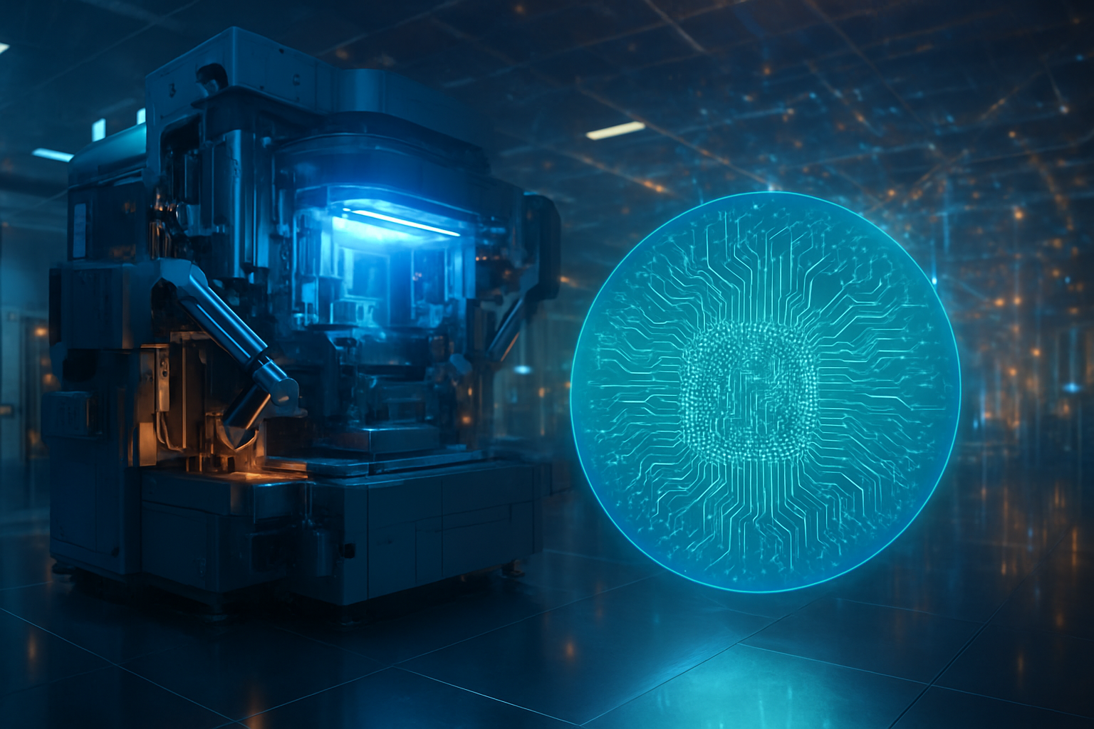
The transition to 2nm is centered at TSMC’s state-of-the-art facilities: the "mother fab" Fab 20 in Baoshan and the newly accelerated Fab 22 in Kaohsiung. By moving from the traditional FinFET (Fin Field-Effect Transistor) structure to a sophisticated Nanosheet Gate-All-Around (GAAFET) architecture, TSMC is providing the efficiency and density required for the next generation of generative AI models and high-performance computing. Early data from the production lines suggest that TSMC has overcome the initial "yield wall" that often plagues new nodes, reporting logic test chip yields between 70% and 80%—a figure that has sent shockwaves through the industry for its unexpected maturity at launch.
Breaking the FinFET Barrier: The Rise of Nanosheet Architecture
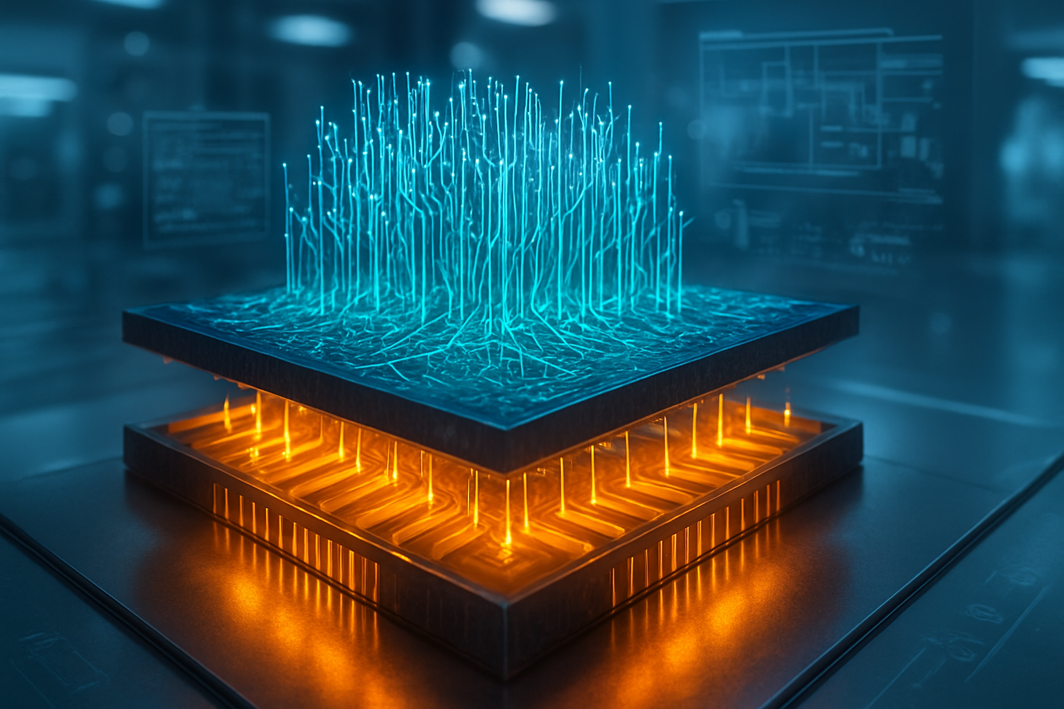
The technical leap from 3nm (N3E) to 2nm (N2) is defined by the shift to GAAFET Nanosheet transistors. Unlike the previous FinFET design, where the gate covers three sides of the channel, the Nanosheet architecture allows the gate to wrap around all four sides. This provides superior electrostatic control, significantly reducing current leakage and allowing for finer tuning of performance. A standout feature of this node is TSMC's "NanoFlex" technology, which provides chip designers with the unprecedented ability to mix and match different nanosheet widths within a single block. This allows engineers to optimize specific areas of a chip for maximum clock speed while keeping other sections optimized for low power consumption, providing a level of granular control that was previously impossible.
The performance gains are substantial: the N2 process offers either a 15% increase in speed at the same power level or a 25% to 30% reduction in power consumption at the same clock frequency compared to the current 3nm technology. Furthermore, the node provides a 1.15x increase in transistor density. While these gains are impressive for mobile devices, they are transformative for the AI sector, where power delivery and thermal management have become the primary bottlenecks for scaling massive data centers.
Initial reactions from the semiconductor research community have been overwhelmingly positive, particularly regarding the 70-80% yield rates. Historically, transitioning to a new transistor architecture like GAAFET has resulted in lower initial yields—competitors like Samsung Electronics (KRX:005930) have famously struggled to stabilize their own GAA processes. TSMC’s ability to achieve high yields in the first month of 2026 suggests a highly refined manufacturing process that will allow for a rapid ramp-up in volume, crucial for meeting the insatiable demand from AI chip designers.
The AI Titans Stake Their Claim
The primary beneficiary of this advancement is Apple (NASDAQ:AAPL), which has reportedly secured the vast majority of the initial 2nm capacity. The upcoming A20 series chips for the iPhone 18 Pro and the M6 series processors for the Mac lineup are expected to be the first consumer products to showcase the N2's efficiency. However, the dynamics of TSMC's customer base are shifting. While Apple was once the undisputed lead customer, Nvidia (NASDAQ:NVDA) has moved into a top-tier partnership role. Following the success of its Blackwell and Rubin architectures, Nvidia's demand for 2nm wafers for its next-generation AI GPUs is expected to rival Apple’s consumption by the end of 2026, as the race for larger and more complex Large Language Models (LLMs) continues.
Other major players like Advanced Micro Devices (NASDAQ:AMD) and Qualcomm (NASDAQ:QCOM) are also expected to pivot toward N2 as capacity expands. The competitive implications are stark: companies that can secure 2nm capacity will have a definitive edge in "performance-per-watt," a metric that has become the gold standard in the AI era. For AI startups and smaller chip designers, the high cost of 2nm—estimated at roughly $30,000 per wafer—may create a wider divide between the industry titans and the rest of the market, potentially leading to further consolidation in the AI hardware space.
Meanwhile, the successful ramp-up puts immense pressure on Intel (NASDAQ:INTC) and Samsung. While Intel has successfully launched its 18A node featuring "PowerVia" backside power delivery, TSMC’s superior yields and massive ecosystem support give it a strategic advantage in terms of reliable volume. Samsung, despite being the first to adopt GAA technology at the 3nm level, continues to face yield challenges, with reports placing their 2nm yields at approximately 50%. This gap reinforces TSMC's position as the "safe" choice for the world’s most critical AI infrastructure.
Geopolitics and the Power of the AI Landscape
The arrival of 2nm mass production is a pivotal moment in the broader AI landscape. We are currently in an era where the software capabilities of AI are outstripping the hardware's ability to run them efficiently. The N2 node is the industry's answer to the "power wall," enabling the creation of chips that can handle the quadrillions of operations required for real-time multimodal AI without melting down data centers or exhausting local batteries. It represents a continuation of Moore’s Law through sheer architectural ingenuity rather than simple scaling.
However, this development also underscores the growing geopolitical and economic concentration of the AI supply chain. With the majority of 2nm production localized in Taiwan's Baoshan and Kaohsiung fabs, the global AI economy remains heavily dependent on a single geographic point of failure. While TSMC is expanding globally, the "leading edge" remains firmly rooted in Taiwan, a fact that continues to influence international trade policy and national security strategies in the U.S., Europe, and China.
Compared to previous milestones, such as the move to EUV (Extreme Ultraviolet) lithography at 7nm, the 2nm transition is more focused on efficiency than raw density. The industry is realizing that the future of AI is not just about fitting more transistors on a chip, but about making sure those transistors can actually be powered and cooled. The 25-30% power reduction offered by N2 is perhaps its most significant contribution to the AI field, potentially lowering the massive carbon footprint associated with training and deploying frontier AI models.
Future Roadmaps: To 1.4nm and Beyond
Looking ahead, the road to even smaller features is already being paved. TSMC has already signaled that its next evolution, N2P, will introduce backside power delivery in late 2026 or early 2027. This will further enhance performance by moving the power distribution network to the back of the wafer, reducing interference with signal routing on the front. Beyond that, the company is already conducting research and development for the A14 (1.4nm) node, which is expected to enter production toward the end of the decade.
The immediate challenge for TSMC and its partners will be capacity management. With the 2nm lines reportedly fully booked through the end of 2026, the industry is watching to see how quickly the Kaohsiung facility can scale to meet the overflow from Baoshan. Experts predict that the focus will soon shift from "getting GAAFET to work" to "how to package it," with advanced 3D packaging technologies like CoWoS (Chip on Wafer on Substrate) playing an even larger role in combining 2nm logic with high-bandwidth memory (HBM).
Predicting the next two years, we can expect a surge in "AI PCs" and mobile devices that can run complex LLMs locally, thanks to the efficiency of 2nm silicon. The challenge will be the cost; as wafer prices climb, the industry must find ways to ensure that the benefits of the Angstrom Era are not limited to the few companies with the deepest pockets.
Conclusion: A Hardware Milestone for History
The commencement of 2nm mass production by TSMC in January 2026 marks a historic turning point for the technology industry. By successfully transitioning to GAAFET architecture with remarkably high yields, TSMC has not only extended its technical leadership but has also provided the essential foundation for the next stage of AI development. The 15% speed boost and 30% power reduction of the N2 node are the catalysts that will allow AI to move from the cloud into every pocket and enterprise across the globe.
In the history of AI, the year 2026 will likely be remembered as the year the hardware finally caught up with the vision. While competitors like Intel and Samsung are making their own strides, TSMC's "Golden Yields" at Baoshan and Kaohsiung suggest that the company will remain the primary architect of the AI era for the foreseeable future.
In the coming months, the tech world will be watching for the first performance benchmarks of Apple’s A20 and Nvidia’s next-generation AI silicon. If these early production successes translate into real-world performance, the shift to 2nm will be seen as the definitive beginning of a new age in computing—one where the limits are defined not by the size of the transistor, but by the imagination of the software running on it.
This content is intended for informational purposes only and represents analysis of current AI developments.
TokenRing AI delivers enterprise-grade solutions for multi-agent AI workflow orchestration, AI-powered development tools, and seamless remote collaboration platforms.
For more information, visit https://www.tokenring.ai/.