On January 15, 2026, the United States and Taiwan signed a landmark bilateral trade and investment agreement, colloquially known as the "Silicon Pact," marking the most significant shift in global technology policy in decades. This historic deal establishes a robust framework for economic integration, capping reciprocal tariffs on Taiwanese goods at 15% while offering aggressive incentives for Taiwanese semiconductor firms to expand their manufacturing footprint on American soil. By providing Section 232 duty exemptions for companies investing in U.S. capacity—up to 2.5 times their planned output—the agreement effectively fast-tracks the "reshoring" of the world’s most advanced chipmaking ecosystem.
The immediate significance of this agreement cannot be overstated. At its core, the deal is a strategic response to the escalating demand for sovereign AI infrastructure. With a staggering $250 billion investment pledge from Taiwan toward U.S. tech sectors, the pact aims to insulate the semiconductor supply chain from geopolitical volatility. For the burgeoning AI industry, which relies almost exclusively on high-end silicon produced in the Taiwan Strait, the agreement provides a much-needed roadmap for stability, ensuring that the hardware necessary for next-generation "GPT-6 class" models remains accessible and secure.
A Technical Blueprint for Semiconductor Sovereignty
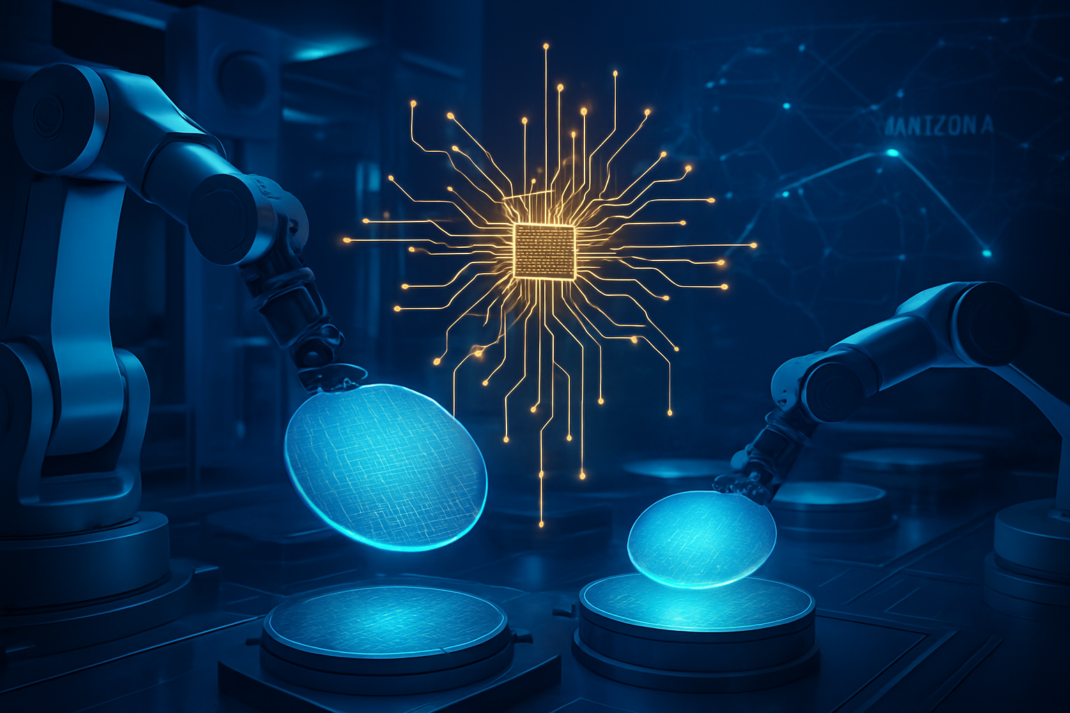
The technical architecture of the "Silicon Pact" is built upon a sophisticated "carrot-and-stick" incentive structure designed to move the center of gravity for high-end manufacturing. Central to this is the utilization of Section 232 of the Trade Expansion Act, which typically allows the U.S. to impose tariffs based on national security. Under the new terms, Taiwanese firms like Taiwan Semiconductor Manufacturing Co. (NYSE: TSM) are granted unprecedented relief: during the construction phase of new U.S. facilities, these firms can import up to 2.5 times their planned capacity duty-free. Once operational, they can maintain a 1.5-to-1 ratio of duty-free imports relative to their local production volume.
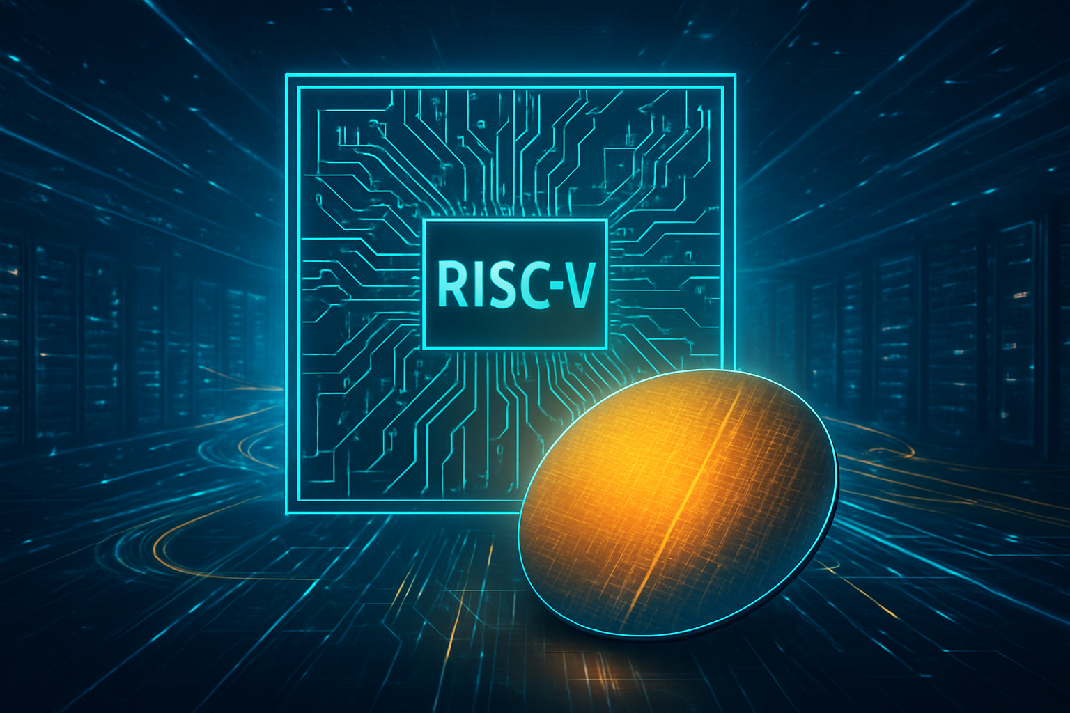
This formula is specifically designed to prevent the "hollow-out" effect while ensuring that the U.S. can meet its immediate demand for advanced nodes. Technical specifications within the pact also emphasize the transition to CoWoS (Chip-on-Wafer-on-Substrate) packaging and 2nm process technologies. By requiring that a significant portion of the advanced packaging process—not just the wafer fabrication—be conducted in the U.S., the agreement addresses the "last mile" bottleneck that has long plagued the domestic semiconductor industry.
Industry experts have noted that this differs from previous initiatives like the 2022 CHIPS Act by focusing heavily on the integration of the entire supply chain rather than just individual fab construction. Initial reactions from the research community have been largely positive, though some analysts point out the immense logistical challenge of migrating the highly specialized Taiwanese labor force and supplier network to hubs in Arizona, Ohio, and Texas. The agreement also includes shared cybersecurity protocols and joint R&D frameworks, creating a unified defense perimeter for intellectual property.
Market Winners and the AI Competitive Landscape
The pact has sent ripples through the corporate world, with major tech giants and AI labs immediately adjusting their 2026-2030 roadmaps. NVIDIA Corporation (NASDAQ: NVDA), the primary beneficiary of high-end AI chips, saw its stock rally as the deal removed a significant "policy overhang" regarding the safety of its supply chain. With the assurance of domestic 3nm and 2nm production for its future architectures, Nvidia can now commit to more aggressive scaling of its AI data center business without the looming threat of sudden trade disruptions.
Other major players like Apple Inc. (NASDAQ: AAPL) and Meta Platforms, Inc. (NASDAQ: META) stand to benefit from the reduced 15% tariff cap, which lowers the cost of importing specialized hardware components and consumer electronics. Startups in the AI space, particularly those focused on custom ASIC (Application-Specific Integrated Circuit) design, are also seeing a strategic advantage. MediaTek (TPE: 2454) has already announced plans for new 2nm collaborations with U.S. tech firms, signaling a shift where Taiwanese design expertise and U.S. manufacturing capacity become more tightly coupled.
However, the deal creates a complex competitive dynamic for major AI labs. While the reshoring effort provides security, the massive capital requirements for building domestic capacity could lead to higher chip prices in the short term. Companies that have already invested heavily in domestic "sovereign AI" projects will find themselves at a distinct market advantage over those relying on unhedged international supply lines. The pact effectively bifurcates the global market, positioning the U.S.-Taiwan corridor as the "gold standard" for high-performance computing hardware.
National Security and the Global AI Landscape
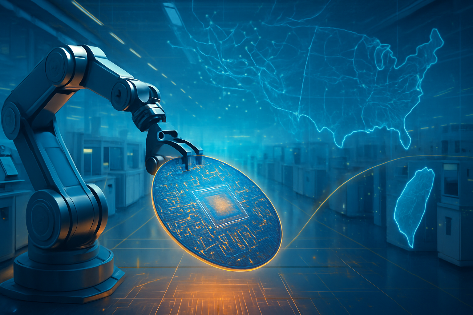
Beyond the balance sheets, the "Silicon Pact" represents a fundamental realignment of the broader AI landscape. By securing 40% of Taiwan's semiconductor supply chain for U.S. reshoring by 2029, the agreement addresses the critical "AI security" concerns that have dominated Washington's policy discussions. In an era where AI dominance is equated with national power, the ability to control the physical hardware of intelligence is seen as a prerequisite for technological leadership. This deal ensures that the U.S. maintains a "hardware moat" against global competitors.
The wider significance also touches on the concept of "friend-shoring." By cementing Taiwan as a top-tier trade partner with tariff parity alongside Japan and South Korea, the U.S. is creating a consolidated technological bloc. This move mirrors previous historic breakthroughs, such as the post-WWII reconstruction of the European industrial base, but with a focus on bits and transistors rather than steel and coal. It is a recognition that in 2026, silicon is the most vital commodity on earth.
Yet, the deal is not without its controversies. In Taiwan, opposition leaders have voiced concerns about the "hollowing out" of the island's industrial crown jewel. Critics argue that the $250 billion in credit guarantees provided by the Taiwanese government essentially uses domestic taxpayer money to subsidize U.S. industrial policy. There are also environmental concerns regarding the massive water and energy requirements of new mega-fabs in arid regions like Arizona, highlighting the hidden costs of reshoring the world's most resource-intensive industry.
The Horizon: Near-Term Shifts and Long-Term Goals
Looking ahead, the next 24 months will be a critical period of "on-ramping" for the Silicon Pact. We expect to see an immediate surge in groundbreaking ceremonies for specialized "satellite" plants—suppliers of ultra-pure chemicals, specialized gases, and lithography components—moving to the U.S. to support the major fabs. Near-term applications will focus on the deployment of Blackwell-successors and the first generation of 2nm-based mobile devices, which will likely feature dedicated on-device AI capabilities that were previously impossible due to power constraints.
In the long term, the pact paves the way for a more resilient, decentralized manufacturing model. Experts predict that the focus will eventually shift from "capacity" to "capability," with U.S.-based labs and Taiwanese manufacturers collaborating on exotic new materials like graphene and photonics-based computing. The challenge will remain the human capital gap; addressing the shortage of specialized semiconductor engineers in the U.S. is a task that no trade deal can solve overnight, necessitating a parallel revolution in technical education and immigration policy.
Conclusion: A New Era of Integrated Technology
The signing of the "Silicon Pact" on January 15, 2026, will likely be remembered as the moment the U.S. and Taiwan codified their technological interdependence for the AI age. By combining massive capital investment, strategic tariff relief, and a focus on domestic manufacturing, the agreement provides a comprehensive answer to the supply chain vulnerabilities exposed over the last decade. It is a $250 billion bet that the future of intelligence must be anchored in secure, reliable, and reshored hardware.
As we move into the coming months, the focus will shift from high-level diplomacy to the grueling work of industrial execution. Investors and industry observers should watch for the first quarterly reports from the "big three" fabs—TSMC, Intel, and Samsung—to see how quickly they leverage the Section 232 exemptions. While the path to full semiconductor sovereignty is long and fraught with technical challenges, the "Silicon Pact" has provided the most stable foundation yet for the next century of AI-driven innovation.
This content is intended for informational purposes only and represents analysis of current AI developments.
TokenRing AI delivers enterprise-grade solutions for multi-agent AI workflow orchestration, AI-powered development tools, and seamless remote collaboration platforms.
For more information, visit https://www.tokenring.ai/.