The global semiconductor landscape has been thrown into chaos this week as a high-stakes trade standoff between Washington and Beijing left the world’s most advanced AI hardware in a state of geopolitical limbo. The "H200 Export Crisis," as it is being called by industry analysts, reached a boiling point following a series of conflicting regulatory maneuvers that have effectively trapped chipmakers in a "regulatory sandwich," threatening the supply chains of the most powerful artificial intelligence models on the planet.
The crisis began when the United States government authorized the export of NVIDIA’s high-end H200 Tensor Core GPUs to China, but only under the condition of a steep 25% national security tariff and a mandatory "vulnerability screening" process on U.S. soil. However, the potential thaw in trade relations was short-lived; within 48 hours, Beijing retaliated by blocking the entry of these chips at customs and issuing a stern warning to domestic tech giants to abandon Western hardware in favor of homegrown alternatives. The resulting stalemate has sent shockwaves through the tech sector, wiping out billions in market value and casting a long shadow over the future of global AI development.
The Hardware at the Heart of the Storm
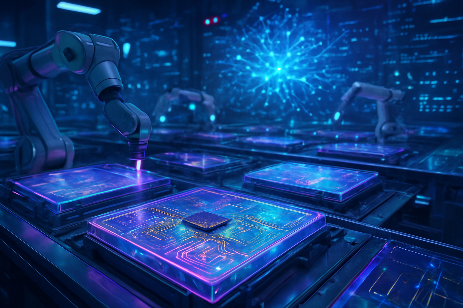
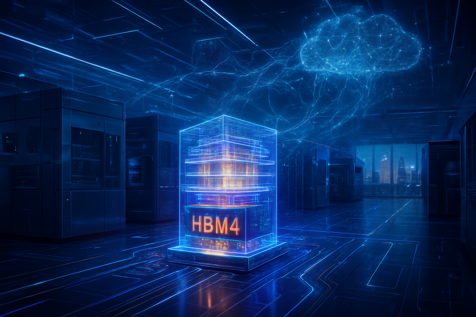
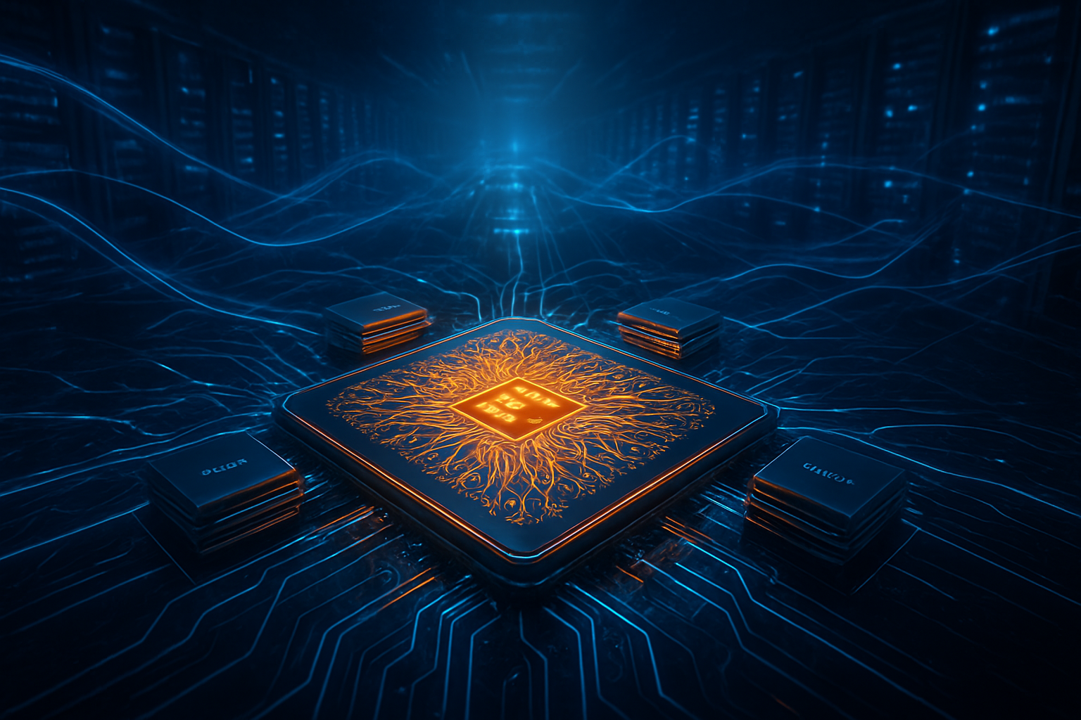
At the center of this geopolitical tug-of-war is the NVIDIA (NASDAQ: NVDA) H200, a powerhouse GPU designed specifically to handle the massive memory requirements of generative AI and large language models (LLMs). Released as an enhancement to the industry-standard H100, the H200 represents a significant technical leap. Its most defining feature is the integration of 141GB of HBM3e memory, providing a staggering 4.8 TB/s of memory bandwidth. This allows the chip to deliver nearly double the inference performance of the H100 for models like Llama 3 and GPT-4, making it the "gold standard" for companies looking to deploy high-speed AI services at scale.
Unlike previous "gimped" versions of chips designed to meet export controls, the H200s in question were intended to be full-specification units. The U.S. Department of Commerce’s decision to allow their export—albeit with a 25% "national security surcharge"—was initially seen as a pragmatic compromise to maintain U.S. commercial dominance while funding domestic chip initiatives. To ensure compliance, the U.S. mandated that chips manufactured by TSMC in Taiwan must first be shipped to U.S.-based laboratories for "security hardening" before being re-exported to China, a logistical hurdle that added weeks to delivery timelines even before the Chinese blockade.
The AI research community has reacted with a mixture of awe and frustration. While the technical capabilities of the H200 are undisputed, researchers in both the East and West fear that the "regulatory sandwich" will stifle innovation. Experts note that AI progress is increasingly dependent on "compute density," and if the most efficient hardware is subject to 25% tariffs and indefinite customs holds, the cost of training next-generation models could become prohibitive for all but the wealthiest entities.
A "Regulatory Sandwich" Squeezes Tech Giants
The term "regulatory sandwich" has become the mantra of 2026, describing the impossible position of firms like NVIDIA and AMD (NASDAQ: AMD). On the top layer, the U.S. government restricts the type of technology that can be sold and imposes heavy financial penalties on permitted transactions. On the bottom layer, the Chinese government is now blocking the entry of that very hardware to protect its own nascent semiconductor industry. For NVIDIA, which saw its stock fluctuate wildly between $187 and $183 this week as the news broke, the Chinese market—once accounting for over a quarter of its data center revenue—is rapidly becoming an inaccessible fortress.
Major Chinese tech conglomerates, including Alibaba (NYSE: BABA), Tencent (HKG: 0700), and ByteDance, are the primary victims of this squeeze. These companies had reportedly earmarked billions for H200 clusters to power their competing LLMs. However, following the U.S. announcement of the 25% tariff, Beijing summoned executives from these firms to "strongly advise" them against fulfilling their orders. The message was clear: purchasing the H200 is now viewed as an act of non-compliance with China’s "Digital Sovereignty" mandate.
This disruption gives a massive strategic advantage to domestic Chinese chip designers like Huawei and Moore Threads. With the H200 officially blocked at the border, Chinese cloud providers have little choice but to pivot to the Huawei Ascend series. While these domestic chips currently trail NVIDIA in raw performance and software ecosystem support, the forced migration caused by the export crisis is providing them with a captive market of the world's largest AI developers, potentially accelerating their development curve by years.
The Bifurcation of the AI Landscape
The H200 crisis is more than a trade dispute; it represents the definitive fracturing of the global AI landscape into two distinct, incompatible stacks. For the past decade, the AI world has operated on a unified foundation of Western hardware and open-source software like NVIDIA's CUDA. The current blockade is forcing China to build a "Parallel Tech Universe," developing its own specialized compilers, libraries, and hardware architectures that do not rely on American intellectual property.
This "bifurcation" carries significant risks. A world with two separate AI ecosystems could lead to a lack of safety standards and interoperability. Furthermore, the 25% U.S. tariff has set a precedent for "tech-protectionism" that could spread to other sectors. Industry veterans compare this moment to the "Sputnik moment" of the 20th century, but with a capitalist twist: the competition isn't just about who gets to the moon first, but who owns the processors that will run the global economy's future intelligence.
Concerns are also mounting regarding the "black market" for chips. As official channels for the H200 close, reports from Hong Kong and Singapore suggest that smaller quantities of these GPUs are being smuggled into mainland China through third-party intermediaries, albeit at markups exceeding 300%. This underground trade undermines the very security goals the U.S. tariffs were meant to achieve, while further inflating costs for legitimate researchers.
What Lies Ahead: From H200 to Blackwell
Looking forward, the immediate challenge for the industry is navigating the "policy whiplash" that has become a staple of 2026. While the H200 is the current flashpoint, NVIDIA’s next-generation "Blackwell" B200 architecture is already looming on the horizon. If the H200—a two-year-old architecture—is causing this level of friction, the export of even more advanced Blackwell chips seems virtually impossible under current conditions.
Analysts predict that NVIDIA may be forced to further diversify its manufacturing base, potentially seeking out "neutral" third-party countries for final assembly and testing to bypass the mandatory U.S. landing requirements. Meanwhile, expect the Chinese government to double down on subsidies for its "National Integrated Circuit Industry Investment Fund" (the Big Fund), aiming to achieve 7nm and 5nm self-sufficiency without Western equipment by 2027. The next few months will likely see a flurry of legal challenges and diplomatic negotiations as both nations realize that a total shutdown of the semiconductor trade is a "mutual-assured destruction" scenario for the digital economy.
A Precarious Path Forward
The H200 export crisis marks a turning point in the history of artificial intelligence. It is the moment when the physical limitations of geopolitics finally caught up with the infinite ambitions of software. The "regulatory sandwich" has proven that even the most innovative companies are not immune to the gravity of national security and trade wars. For NVIDIA, the loss of the Chinese market represents a multi-billion dollar hurdle that must be cleared through even faster innovation in the Western and Middle Eastern markets.
As we move deeper into 2026, the tech industry will be watching the delivery of the first "security-screened" H200s to see if any actually make it past Chinese customs. If the blockade holds, we are witnessing the birth of a truly decoupled tech world. Investors and developers alike should prepare for a period of extreme volatility, where a single customs directive can be as impactful as a technical breakthrough.
This content is intended for informational purposes only and represents analysis of current AI developments.
TokenRing AI delivers enterprise-grade solutions for multi-agent AI workflow orchestration, AI-powered development tools, and seamless remote collaboration platforms.
For more information, visit https://www.tokenring.ai/.