In a move that underscores the relentless demand for artificial intelligence and high-performance computing, Taiwan Semiconductor Manufacturing Company (NYSE: TSM) has announced a record-shattering capital expenditure budget of up to $56 billion for 2026. This massive financial commitment represents a nearly 40% increase over the previous year, signaling TSMC’s intent to cement its dominance as the world’s premier foundry at a time when silicon has become the most vital resource in the global economy.
The crown jewel of this expansion is a dramatic $17 billion upgrade to the company’s second fabrication facility in Kumamoto, Japan. Following a high-level meeting between TSMC CEO C.C. Wei and Japanese Prime Minister Sanae Takaichi on February 5, 2026, the company confirmed that the facility—originally slated for mature nodes—will now produce cutting-edge 3-nanometer (3nm) chips. This pivot not only marks the first time TSMC has exported its most advanced mass-production technology to Japan but also serves as the cornerstone for Japan’s "semiconductor rebirth," securing the nation's position as a tier-1 manufacturing hub for the AI era.
The 3nm Leap: Technical Sophistication and the Kumamoto Upgrade
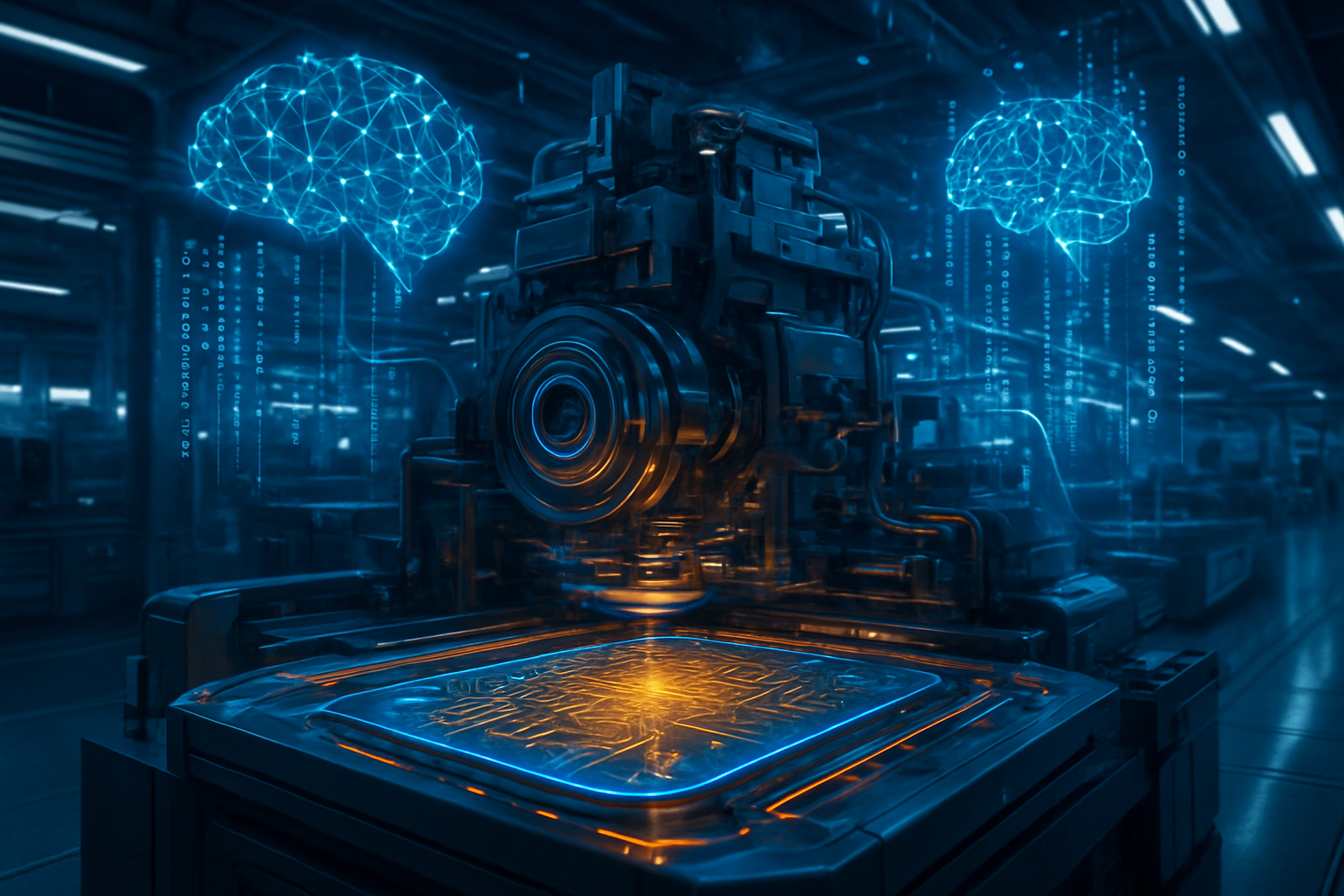
The decision to bring 3nm technology to the second Kumamoto facility, operated under the JASM (Japan Advanced Semiconductor Manufacturing) joint venture, represents a massive technological leap from initial plans. Originally envisioned to handle 6nm to 12nm "specialty" nodes for automotive and industrial sectors, the $17 billion investment (approximately ¥2.6 trillion) transforms the site into a world-class advanced logic powerhouse. The 3nm process, utilizing FinFET (Fin Field-Effect Transistor) architecture at its most refined stage, offers a 15% speed improvement at the same power or a 30% power reduction at the same speed compared to the 5nm generation, along with a 1.6x increase in logic density.
The upgrade is a direct response to the "insatiable" demand for AI accelerators and next-generation mobile processors. By situating 3nm production in Japan, TSMC is effectively decentralizing its most advanced manufacturing capabilities away from Taiwan for the first time in history. The facility is expected to enter mass production by late 2027, utilizing the latest in Extreme Ultraviolet (EUV) lithography tools. This move is supported by a massive expansion in TSMC’s advanced packaging capacity, with 10% to 20% of the total $56 billion CapEx dedicated to CoWoS (Chip on Wafer on Substrate) and other "3D" packaging technologies, which are essential for the massive memory-and-logic sandwiches that power large language models.
Initial reactions from the semiconductor research community suggest that TSMC’s aggressive spending is a preemptive strike against competitors. While Intel (NASDAQ: INTC) and Samsung (KRX: 005930) are racing to stabilize their own advanced nodes, TSMC’s ability to allocate over $50 billion in a single year—more than the total market capitalization of many mid-sized tech firms—creates a formidable "moat of capital" that is difficult for any rival to bridge.
Strategic Advantage: Powering the AI Giants and Reshaping the Market
This massive capital injection directly benefits the world’s leading technology companies, particularly those in the "Magnificent Seven" and the broader AI ecosystem. Companies like Nvidia (NASDAQ: NVDA), Apple (NASDAQ: AAPL), and Advanced Micro Devices (NASDAQ: AMD) are the primary consumers of TSMC’s advanced nodes. With the $56 billion CapEx, TSMC is effectively guaranteeing these giants that the capacity for their next-generation AI GPUs and custom silicon will be available, mitigating the supply chain bottlenecks that defined the 2023-2025 period.
The investment in Japan provides a strategic hedge for global tech companies concerned about geopolitical stability in the Taiwan Strait. For Apple and Nvidia, having a 3nm source in a stable, high-infrastructure country like Japan provides a "Plan B" that was previously unavailable. This diversification is expected to disrupt the current market positioning of competitors; as TSMC solidifies its role as the de facto "Central Bank of Silicon," it puts immense pressure on Intel’s Foundry Services to deliver on their "18A" node promises or risk losing further market share in the premium AI segment.
Furthermore, Japan’s automotive and robotics giants, such as Toyota (NYSE: TM) and Sony (NYSE: SONY), stand to gain significantly. By having a 3nm foundry in their backyard, these companies can integrate high-performance AI directly into their hardware with lower latency and more secure supply chains, potentially leading to a new generation of autonomous vehicles and sophisticated industrial robotics that were previously limited by chip availability.
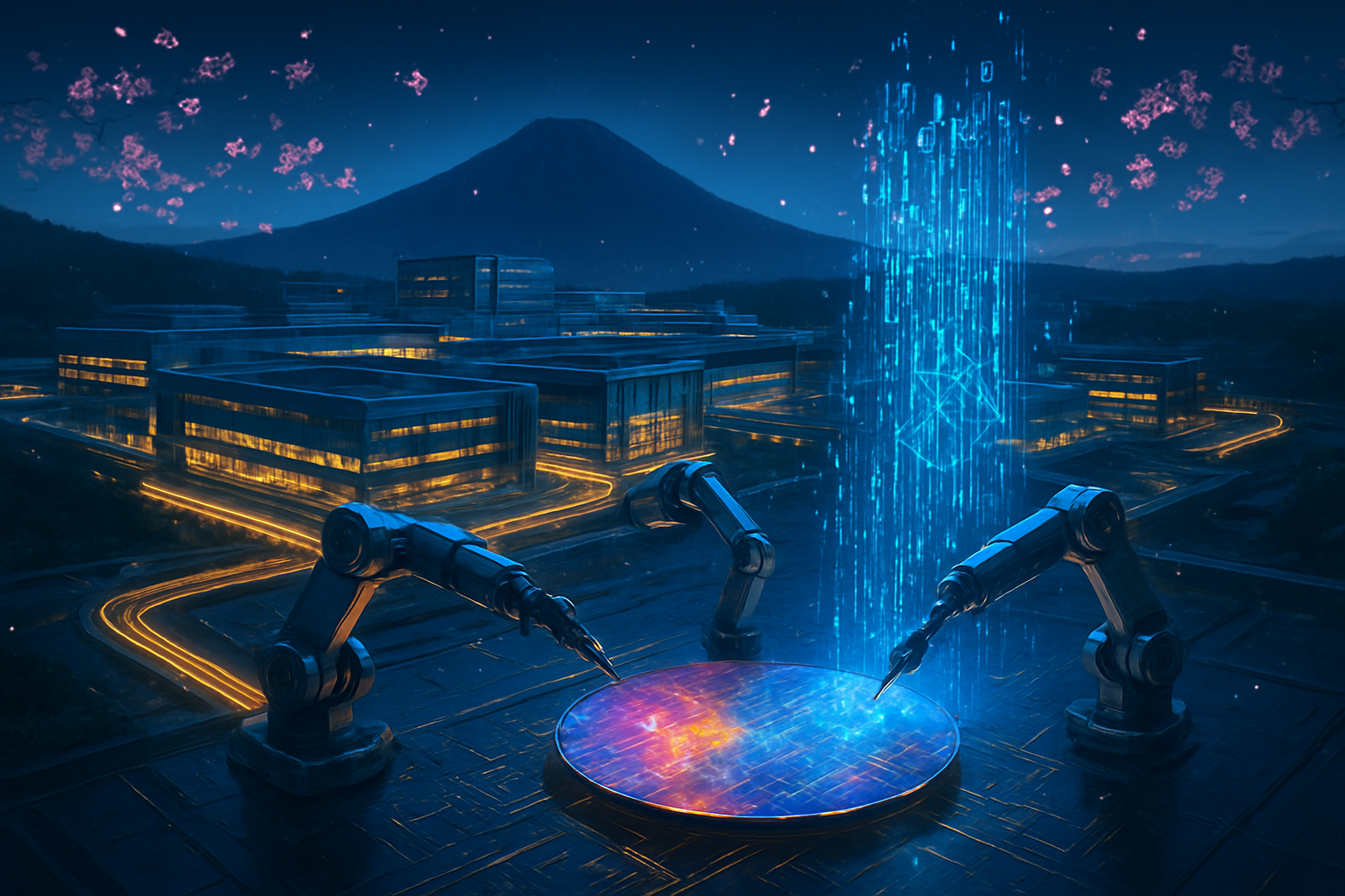
A "Silicon Island" Reborn: Global Economic Security and Geopolitics
The significance of the Kumamoto expansion extends far beyond corporate balance sheets; it is a geopolitical masterstroke. CEO C.C. Wei’s visit to the Prime Minister’s office on February 5, 2026, highlighted a new era of "semiconductor diplomacy." Prime Minister Sanae Takaichi’s government has made the semiconductor industry a matter of national security, increasing the Ministry of Economy, Trade and Industry (METI) budget for chips and AI to a staggering ¥1.23 trillion for fiscal 2026.
This "Semiconductor Rebirth Strategy" aims to restore Japan to the prominence it held in the 1980s. By hosting a 3nm facility, Kumamoto is being transformed into a "Silicon Island," attracting a cluster of chemical suppliers, equipment manufacturers, and top-tier engineering talent. This concentration of resources is a critical component of global economic security, creating a more resilient supply chain that is less dependent on any single geographic point of failure.
However, the move is not without its concerns. Critics point to the immense subsidies required—Japan has already committed trillions of yen to attract TSMC—and question whether such "state-led growth" can be sustained. There are also environmental concerns regarding the massive water and electricity requirements of a 3nm facility. Nonetheless, compared to the risks of a "silicon drought," the Japanese government clearly views these costs as a necessary premium for national sovereignty in the digital age.
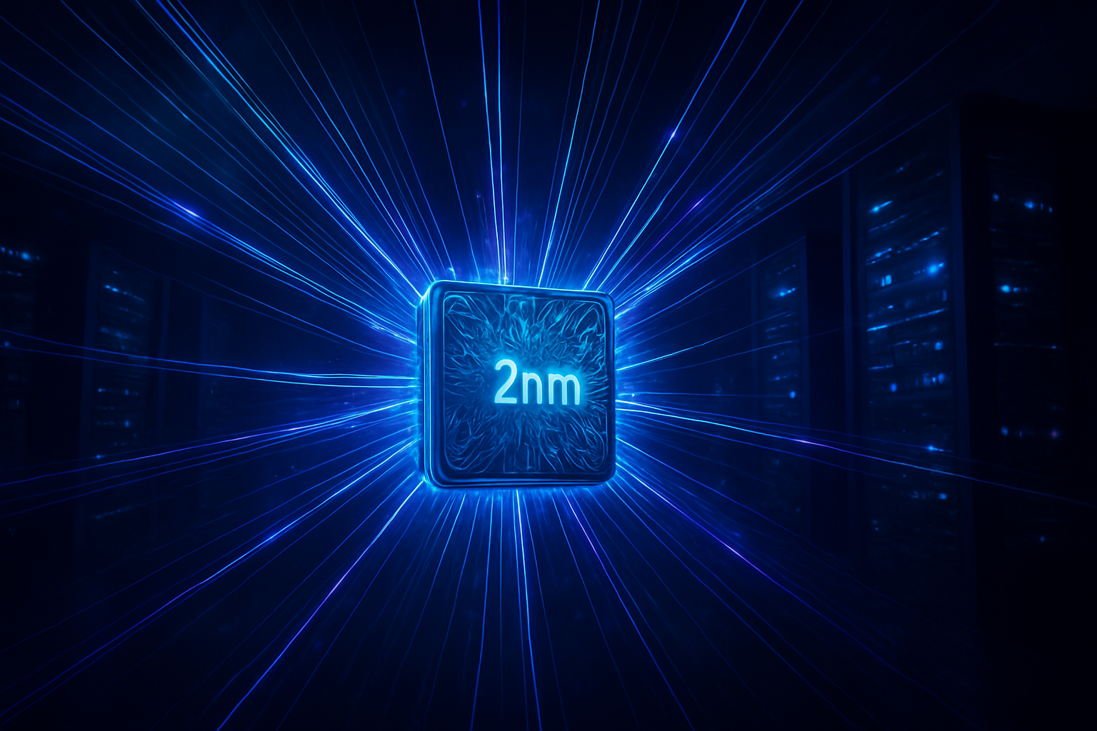
The Road to 2nm: What Lies Ahead for TSMC and Japan
Looking forward, the $56 billion CapEx is just the beginning of a multi-year roadmap that leads toward 2-nanometer (2nm) technology. While Kumamoto is being outfitted for 3nm, TSMC’s facilities in Hsinchu and Kaohsiung, Taiwan, are already preparing for the transition to 2nm and "GAA" (Gate-All-Around) transistor architectures. Experts predict that the lessons learned from the 3nm Kumamoto facility will eventually pave the way for a 2nm upgrade in Japan by the end of the decade.
The next major challenge for TSMC and its partners will be the integration of "Next-Gen" domestic ventures. Japan’s state-backed Rapidus is still pursuing its goal of 2nm production in Hokkaido by 2027. While some see Rapidus and TSMC as competitors, the sheer volume of the AI market suggests a "co-opetition" model, where TSMC handles the massive commercial volume and Rapidus focuses on high-speed, specialized prototyping.
The primary hurdle in the near term will be human capital. The demand for semiconductor engineers in Japan is expected to reach an all-time high by 2027, necessitating a massive overhaul of university curricula and an increase in international talent recruitment. How Japan and TSMC address this "talent gap" will determine whether the $17 billion Kumamoto facility reaches its full operational potential.
Conclusion: A Watershed Moment for the Global Tech Order
TSMC’s $56 billion capital expenditure plan and the $17 billion 3nm upgrade in Japan represent a watershed moment in the history of technology. It is a definitive statement that the AI revolution is not a temporary bubble but a fundamental shift in the global industrial landscape. By decentralizing its most advanced manufacturing and aligning itself with Japan's "semiconductor rebirth," TSMC is redrawing the map of the digital world.
The key takeaways are clear: the barrier to entry for leading-edge chip manufacturing is now so high that only a handful of nations and companies can participate. For Japan, this is a return to form; for TSMC, it is a strategic expansion that balances growth with risk management; and for the global AI industry, it is the fuel needed for the next decade of innovation.
In the coming months, watchers should look for the finalized subsidy packages from the Japanese government and the first shipments of EUV tools to Kumamoto. As construction begins on the 3nm extension, the "Silicon Island" of Kyūshū will be the most important construction site on the planet, determining the pace of progress for the entire AI-driven future.
This content is intended for informational purposes only and represents analysis of current AI developments.
TokenRing AI delivers enterprise-grade solutions for multi-agent AI workflow orchestration, AI-powered development tools, and seamless remote collaboration platforms.
For more information, visit https://www.tokenring.ai/.