Tag: Semiconductors

  • Arm’s Strategic Pivot: Acquiring DreamBig Semiconductor to Lead the AI Networking Era

    Arm’s Strategic Pivot: Acquiring DreamBig Semiconductor to Lead the AI Networking Era

    In a move that signals a fundamental shift in the architecture of artificial intelligence infrastructure, Arm Holdings plc (NASDAQ: ARM) has moved to acquire DreamBig Semiconductor, a specialized startup at the forefront of high-performance AI networking and chiplet-based interconnects. Announced in late 2025 and currently moving toward a final close in March 2026, the $265 million deal marks Arm’s transition from a provider of general-purpose CPU "blueprints" to a holistic architect of the data center. By integrating DreamBig’s advanced Data Processing Unit (DPU) and SmartNIC technology, Arm is positioning itself to own the "connective tissue" that binds thousands of processors into the massive AI clusters required for the next generation of generative models.

    The acquisition comes at a pivotal moment as the industry moves away from a CPU-centric model toward a data-centric one. As the parent company SoftBank Group Corp (TYO: 9984) continues to push Arm toward higher-margin system-level offerings, the integration of DreamBig provides the essential networking fabric needed to compete with vertical giants. This move is not merely a product expansion; it is a defensive and offensive masterstroke aimed at securing Arm’s dominance in the custom silicon era, where the ability to move data efficiently is becoming more valuable than the raw speed of the processor itself.

    The Technical Core: Mercury SuperNICs and the MARS Chiplet Hub

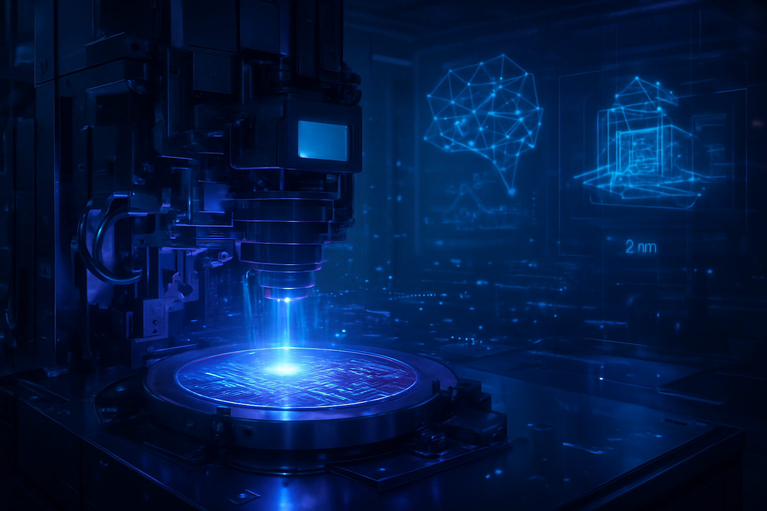
    The technical centerpiece of this acquisition is DreamBig’s Mercury AI-SuperNIC. Unlike traditional network interface cards designed for general web traffic, the Mercury platform is purpose-built for the brutal demands of GPU-to-GPU communication. It supports bandwidths up to 800 Gbps and utilizes a hardware-accelerated Remote Direct Memory Access (RDMA) engine. This allows AI accelerators to exchange data directly across a network without involving the host CPU, eliminating a massive source of latency that has historically plagued large-scale training clusters. By bringing this IP in-house, Arm can now offer its partners a "Total Design" package that includes both the Neoverse compute cores and the high-speed networking required to link them.

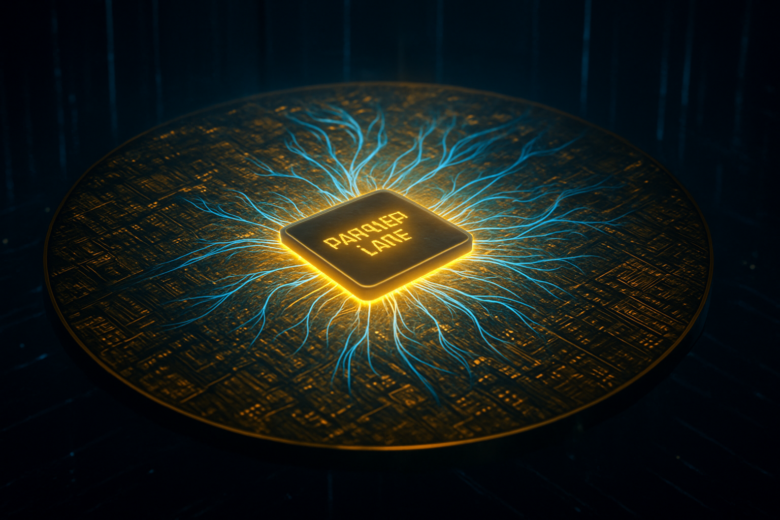
    Beyond the NIC, DreamBig’s MARS Chiplet Platform offers a groundbreaking approach to memory bottlenecks. The platform features the "Deimos Chiplet Hub," which enables the 3D stacking of High Bandwidth Memory (HBM) directly onto the networking or compute die. This architecture can support a staggering 12.8 Tbps of total bandwidth. In the context of previous technology, this represents a significant departure from monolithic chip designs, allowing for a modular, "mix-and-match" approach to silicon. This modularity is essential for AI inference, where the ability to feed data to the processor quickly is often the primary limiting factor in performance.

    Industry experts have noted that this acquisition effectively fills the largest gap in Arm’s portfolio. While Arm has long dominated the power-efficiency side of the equation, it lacked the proprietary interconnect technology held by rivals like NVIDIA Corporation (NASDAQ: NVDA) with its Mellanox/ConnectX line or Marvell Technology, Inc. (NASDAQ: MRVL). Initial reactions from the research community suggest that Arm’s new "Networking-on-a-Chip" capabilities could reduce the energy overhead of data movement in AI clusters by as much as 30% to 50%, a critical improvement as data centers face increasingly stringent power limits.

    Shifting the Competitive Landscape: Hyperscalers and the RISC-V Threat

    The strategic implications of this deal extend directly into the boardrooms of the "Cloud Titans." Companies like Amazon.com, Inc. (NASDAQ: AMZN), Alphabet Inc. (NASDAQ: GOOGL), and Microsoft Corp. (NASDAQ: MSFT) have already moved toward designing their own custom silicon—such as AWS Graviton, Google Axion, and Azure Cobalt—to reduce their reliance on expensive merchant silicon. By acquiring DreamBig, Arm is essentially providing a "starter kit" for these hyperscalers to build their own DPUs and networking stacks, similar to the specialized Nitro system developed by AWS. This levels the playing field, allowing smaller cloud providers and enterprise data centers to deploy custom, high-performance AI infrastructure that was previously the sole domain of the world’s largest tech companies.

    Furthermore, this acquisition is a direct response to the rising challenge of RISC-V architecture. The open-standard RISC-V has gained significant momentum due to its modularity and lack of licensing fees, recently punctuated by Qualcomm Inc. (NASDAQ: QCOM) acquiring the RISC-V leader Ventana Micro Systems in late 2025. By offering DreamBig’s chiplet-based interconnects alongside its CPU IP, Arm is neutralizing one of RISC-V’s biggest advantages: the ease of customization. Arm is telling its customers that they no longer need to switch to RISC-V to get modular, specialized networking; they can get it within the mature, software-rich Arm ecosystem.

    The market positioning here is clear: Arm is evolving from a component vendor into a systems company. This puts them on a collision course with NVIDIA, which has used its proprietary NVLink interconnect to maintain a "moat" around its GPUs. By providing an open yet high-performance alternative through the DreamBig technology, Arm is enabling a more heterogeneous AI ecosystem where chips from different vendors can talk to each other as efficiently as if they were on the same piece of silicon.

    The Broader AI Landscape: The End of the Standalone CPU

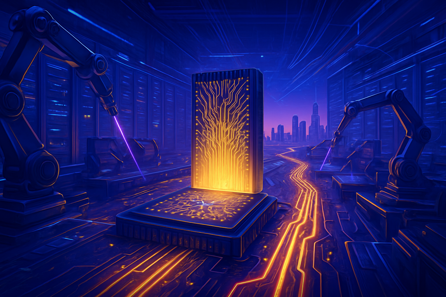
    This development fits into a broader trend where the "system is the new chip." In the early days of the AI boom, the industry focused almost exclusively on the GPU. However, as models have grown to trillions of parameters, the bottleneck has shifted from computation to communication. Arm’s acquisition of DreamBig highlights the reality that in 2026, an AI strategy is only as good as its networking fabric. This mirrors previous industry milestones, such as NVIDIA’s acquisition of Mellanox in 2019, but with a focus on the custom silicon market rather than off-the-shelf hardware.

    The environmental impact of this shift cannot be overstated. As AI data centers begin to consume a double-digit percentage of global electricity, the efficiency gains promised by integrated Arm-plus-Networking architectures are a necessity, not a luxury. By reducing the distance and the energy required to move a bit of data from memory to the processor, Arm is addressing the primary sustainability concern of the AI era. However, this consolidation also raises concerns about market power. As Arm moves deeper into the system stack, the barriers to entry for new silicon startups may become even higher, as they will now have to compete with a fully integrated Arm ecosystem.

    Future Horizons: 1.6 Terabit Networking and Beyond

    Looking ahead, the integration of DreamBig technology is expected to accelerate the roadmap for 1.6 Tbps networking, which experts predict will become the standard for ultra-large-scale training by 2027. We can expect to see Arm-branded "compute-and-connect" chiplets appearing in the market by late 2026, allowing companies to assemble AI servers with the same ease as building a PC. There is also significant potential for this technology to migrate into "Edge AI" applications, where low-power, high-bandwidth interconnects could enable sophisticated autonomous systems and private AI clouds.

    The next major challenge for Arm will be the software layer. While the hardware specifications of the Mercury and MARS platforms are impressive, their success will depend on how well they integrate with existing AI frameworks like PyTorch and JAX. We should expect Arm to launch a massive software initiative in the coming months to ensure that developers can take full advantage of the RDMA and memory-stacking features without having to rewrite their codebases. If successful, this could create a "virtuous cycle" of adoption that cements Arm’s place at the heart of the AI data center for the next decade.

    Conclusion: A New Chapter for the Silicon Ecosystem

    The acquisition of DreamBig Semiconductor is a watershed moment for Arm Holdings. It represents the completion of its transition from a mobile-centric IP designer to a foundational architect of the global AI infrastructure. By securing the technology to link processors at extreme speeds and with record efficiency, Arm has effectively shielded itself from the modular threat of RISC-V while providing its largest customers with the tools they need to break free from proprietary hardware silos.

    As we move through 2026, the key metric to watch will be the adoption rate of the Arm Total Design program. If major hyperscalers and emerging AI labs begin to standardize on Arm’s networking IP, the company will have successfully transformed the data center into an Arm-first environment. This development doesn't just change how chips are built; it changes how the world’s most powerful AI models are trained and deployed, making the "AI-on-Arm" vision an inevitable reality.


    This content is intended for informational purposes only and represents analysis of current AI developments.

    TokenRing AI delivers enterprise-grade solutions for multi-agent AI workflow orchestration, AI-powered development tools, and seamless remote collaboration platforms.
    For more information, visit https://www.tokenring.ai/.

  • ASML Enters the “Angstrom Era”: How Intel and TSMC’s Record Capex is Fueling the High-NA EUV Revolution

    ASML Enters the “Angstrom Era”: How Intel and TSMC’s Record Capex is Fueling the High-NA EUV Revolution

    As the global technology industry crosses into 2026, ASML (NASDAQ:ASML) has officially cemented its role as the ultimate gatekeeper of the artificial intelligence revolution. Following a fiscal 2025 that saw unprecedented demand for AI-specific silicon, ASML’s 2026 outlook points to a historic revenue target of €36.5 billion. This growth is being propelled by a massive capital expenditure surge from industry titans Intel (NASDAQ:INTC) and TSMC (NYSE:TSM), who are locked in a high-stakes "Race to 2nm" and beyond. The centerpiece of this transformation is the transition of High-NA (Numerical Aperture) Extreme Ultraviolet (EUV) lithography from experimental pilot lines into high-volume manufacturing (HVM).

    The immediate significance of this development cannot be overstated. With Big Tech projected to invest over $400 billion in AI infrastructure in 2026 alone, the bottleneck has shifted from software algorithms to the physical limits of silicon. ASML’s delivery of the Twinscan EXE:5200 systems represents the first time the semiconductor industry can reliably print features at the angstrom scale in a commercial environment. This technological leap is the primary engine allowing chipmakers to keep pace with the exponential compute requirements of next-generation Large Language Models (LLMs) and autonomous AI agents.

    The Technical Edge: Twinscan EXE:5200 and the 8nm Resolution Frontier

    At the heart of the 2026 roadmap is the Twinscan EXE:5200, ASML’s flagship High-NA EUV system. Unlike the previous generation of standard (Low-NA) EUV tools that utilized a 0.33 numerical aperture, the High-NA systems utilize a 0.55 NA lens system. This allows for a resolution of 8nm, enabling the printing of features that are 1.7 times smaller than what was previously possible. For engineers, this means the ability to achieve a 2.9x increase in transistor density without the need for complex, yield-killing multi-patterning techniques.

    The EXE:5200 is a significant upgrade over the R&D-focused EXE:5000 models delivered in 2024 and 2025. It boasts a productivity throughput of over 200 wafers per hour (WPH), matching the efficiency of standard EUV tools while operating at a far tighter resolution. This throughput is critical for the commercial viability of 2nm and 1.4nm (14A) nodes. By moving to a single-exposure process for the most critical metal layers of a chip, manufacturers can reduce cycle times and minimize the cumulative defects that occur when a single layer must be passed through a scanner multiple times.

    Initial reactions from the industry have been polarized along strategic lines. Intel, which received the world’s first commercial-grade EXE:5200B in late 2025, has championed the tool as the "holy grail" of process leadership. Conversely, experts at TSMC initially expressed caution regarding the system's $400 million price tag, preferring to push standard EUV to its absolute limits. However, as of early 2026, the sheer complexity of 1.6nm (A16) and 1.4nm designs has forced a universal consensus: High-NA is no longer an optional luxury but a fundamental requirement for the "Angstrom Era."

    Strategic Warfare: Intel’s First-Mover Gamble vs. TSMC’s Efficiency Engine

    The competitive landscape of 2026 is defined by a sharp divergence in how the world’s two largest foundries are deploying ASML’s technology. Intel has adopted an aggressive "first-mover" strategy, utilizing High-NA EUV to accelerate its 14A (1.4nm) node. By integrating these tools earlier than its rivals, Intel aims to reclaim the process leadership it lost a decade ago. For Intel, 2026 is the "prove-it" year; if the EXE:5200 can deliver superior yields for its Panther Lake and Clearwater Forest processors, the company will have a strategic advantage in attracting external foundry customers like Microsoft (NASDAQ:MSFT) and Nvidia (NASDAQ:NVDA).

    TSMC, meanwhile, is operating with a massive 2026 capex budget of $52 billion to $56 billion, much of which is dedicated to the high-volume ramp of its N2 (2nm) and N2P nodes. While TSMC has been more conservative with High-NA adoption—relying on standard EUV with advanced multi-patterning for its A16 (1.6nm) process—the company has begun installing High-NA evaluation tools in early 2026 to de-risk its future A10 node. TSMC’s strategy focuses on maximizing the ROI of its existing EUV fleet while maintaining its dominant 90% market share in high-end AI accelerators.

    This shift has profound implications for chip designers. Nvidia’s "Rubin" R100 architecture and AMD’s (NASDAQ:AMD) MI400 series, both expected to dominate 2026 data center sales, are being optimized for these new nodes. While Nvidia is currently leveraging TSMC’s 3nm N3P process, rumors suggest a split-foundry strategy may emerge by the end of 2026, with some high-performance components being shifted to Intel’s 18A or 14A lines to ensure supply chain resiliency.

    The Triple Threat: 2nm, Advanced Packaging, and the Memory Supercycle

    The 2026 outlook is not merely about smaller transistors; it is about "System-on-Package" (SoP) innovation. Advanced packaging has become a third growth lever for ASML. Techniques like TSMC’s CoWoS-L (Chip-on-Wafer-on-Substrate with Local Silicon Interconnect) are now scaling to 5.5x the reticle limit, allowing for massive AI "Super-Chips" that combine logic, cache, and HBM4 (High Bandwidth Memory) in a single massive footprint. ASML has responded by launching specialized scanners like the Twinscan XT:260, designed specifically for the high-precision alignment required in 3D stacking and hybrid bonding.

    The memory sector is also becoming an "EUV-intensive" business. SK Hynix (KRX:000660) and Samsung (KRX:005930) are in the midst of an HBM-led supercycle, where the logic base dies for HBM4 are being manufactured on advanced logic nodes (5nm and 12nm). This has created a secondary surge in orders for ASML’s standard EUV systems. For the first time in history, the demand for lithography tools is being driven equally by memory density and logic performance, creating a diversified revenue stream that insulates ASML from downturns in the consumer smartphone or PC markets.

    However, this transition is not without concerns. The extreme cost of High-NA systems and the energy required to run them are putting pressure on the margins of smaller players. Industry analysts worry that the "Angstrom Era" may lead to further consolidation, as only a handful of companies can afford the $20+ billion price tag of a modern "Mega-Fab." Geopolitical tensions also remain a factor, as ASML continues to navigate strict export controls that have drastically reduced its revenue from China, forcing the company to rely even more heavily on the U.S., Taiwan, and South Korea.

    Future Horizons: The Path to 1nm and the Glass Substrate Pivot

    Looking beyond 2026, the trajectory for lithography points toward the sub-1nm frontier. ASML is already in the early R&D phases for "Hyper-NA" systems, which would push the numerical aperture to 0.75. Near-term, we expect to see the full stabilization of High-NA yields by the third quarter of 2026, followed by the first 1.4nm (14A) risk production runs. These developments will be essential for the next generation of AI hardware capable of on-device "reasoning" and real-time multimodal processing.

    Another development to watch is the shift toward glass substrates. Led by Intel, the industry is beginning to replace organic packaging materials with glass to provide the structural integrity needed for the increasingly heavy and hot AI chip stacks. ASML’s packaging-specific lithography tools will play a vital role here, ensuring that the interconnects on these glass substrates can meet the nanometer-perfect alignment required for copper-to-copper hybrid bonding. Experts predict that by 2028, the distinction between "front-end" wafer fabrication and "back-end" packaging will have blurred entirely into a single, continuous manufacturing flow.

    Conclusion: ASML’s Indispensable Decade

    As we move through 2026, ASML stands at the center of the most aggressive capital expansion in industrial history. The transition to High-NA EUV with the Twinscan EXE:5200 is more than just a technical milestone; it is the physical foundation upon which the next decade of artificial intelligence will be built. With a €33 billion order backlog and a dominant position in both logic and memory lithography, ASML is uniquely positioned to benefit from the "AI Infrastructure Supercycle."

    The key takeaway for 2026 is that the industry has successfully navigated the "air pocket" of the early 2020s and is now entering a period of normalized, high-volume growth. While the "Race to 2nm" will produce clear winners and losers among foundries, the collective surge in capex ensures that the compute bottleneck will continue to widen, making way for AI models of unprecedented scale. In the coming months, the industry will be watching Intel’s 18A yield reports and TSMC’s A16 progress as the definitive indicators of who will lead the angstrom-scale future.


    This content is intended for informational purposes only and represents analysis of current AI developments.

    TokenRing AI delivers enterprise-grade solutions for multi-agent AI workflow orchestration, AI-powered development tools, and seamless remote collaboration platforms.
    For more information, visit https://www.tokenring.ai/.

  • The Silicon Renaissance: How Generative AI Matured to Master the 2nm Frontier in 2026

    The Silicon Renaissance: How Generative AI Matured to Master the 2nm Frontier in 2026

    As of January 2026, the semiconductor industry has officially crossed a Rubicon that many thought would take decades to reach: the full maturity of AI-driven chip design. The era of manual "trial and error" in transistor layout has effectively ended, replaced by an autonomous, generative design paradigm that has made the mass production of 2nm process nodes not only possible but commercially viable. Leading the charge are Electronic Design Automation (EDA) titans Synopsys (NASDAQ: SNPS) and Cadence Design Systems (NASDAQ: CDNS), which have successfully transitioned from providing "AI-assisted" tools to deploying fully "agentic" AI systems that reason, plan, and execute complex chip architectures with minimal human intervention.

    This transition marks a pivotal moment for the global tech economy. In early 2026, the integration of generative AI into EDA workflows has slashed design cycles for flagship processors from years to months. With the 2nm node introducing radical physical complexities—such as Gate-All-Around (GAA) transistors and Backside Power Delivery Networks (BSPDN)—the sheer mathematical density of modern chips had reached a "complexity wall." Without the generative breakthroughs seen this year, the industry likely would have faced a multi-year stagnation in Moore’s Law; instead, AI has unlocked a new trajectory of performance and energy efficiency.

    Autonomous Agents and Generative Migration: The Technical Breakthroughs

    The technical centerpiece of 2026 is the emergence of "Agentic Design." Synopsys (NASDAQ: SNPS) recently unveiled AgentEngineer™, a flagship advancement within its Synopsys.ai suite. Unlike previous generative AI that merely suggested code snippets, AgentEngineer utilizes autonomous AI agents capable of high-level reasoning. These agents can independently handle "high-toil" tasks such as complex Design Rule Checking (DRC) and layout optimization for the ultra-sensitive 2nm GAA architectures. By simulating billions of layout permutations in a fraction of the time required by human engineers, Synopsys reports that these tools can compress 2nm development cycles by an estimated 12 months, effectively allowing a three-year R&D roadmap to be completed in just two.

    Simultaneously, Cadence Design Systems (NASDAQ: CDNS) has revolutionized the industry with its JedAI (Joint Enterprise Data and AI) platform and its generative node-to-node migration tools. In the 2026 landscape, a major bottleneck for chip designers was moving legacy 5nm or 3nm intellectual property (IP) to the new 2nm and A16 (1.6nm) nodes. Cadence's generative AI now allows for the automatic migration of these designs while preserving performance integrity, reducing the time required for such transitions by up to 4x. This is further bolstered by their reinforcement-learning engine, Cerebrus, which Samsung (OTC: SSNLF) recently credited with achieving a 22% power reduction on its latest 2nm-class AI accelerators.

    The technical specifications of these systems are staggering. The 2026 versions of these EDA tools now incorporate "Multiphysics AI" through integrations like the Synopsys-Ansys (NASDAQ: ANSS) merger, allowing for real-time analysis of heat, stress, and electromagnetic interference as the AI draws the chip. This holistic approach is critical for the 3D-stacked chips that have become standard in 2026, where traditional 2D routing no longer suffices. The AI doesn't just place transistors; it predicts how they will warp under thermal load before a single atom of silicon is ever etched.

    The Competitive Landscape: Winners in the 2nm Arms Race

    The primary beneficiaries of this AI maturity are the major foundries and the hyperscale "fabless" giants. TSMC (NYSE: TSM), Samsung, and Intel (NASDAQ: INTC) have all integrated these AI-agentic flows into their reference designs for 2026. For tech giants like Nvidia (NASDAQ: NVDA), Apple (NASDAQ: AAPL), and Advanced Micro Devices (NASDAQ: AMD), the ability to iterate on 2nm designs every six months rather than every two years has fundamentally altered their product release cadences. We are now seeing a shift toward more specialized, application-specific silicon (ASICs) because the cost and time of designing a custom chip have plummeted thanks to AI automation.

    The competitive implications are stark. Smaller startups that previously could not afford the multi-hundred-million-dollar design costs associated with leading-edge nodes are now finding a foothold. AI-driven EDA tools have effectively democratized high-end silicon design, allowing a lean team of engineers to produce chips that would have required a thousand-person department in 2022. This disruption is forcing traditional semiconductor giants to pivot toward "AI-first" internal workflows to maintain their strategic advantage.

    Furthermore, the rise of Japan’s Rapidus—which in 2026 is using specialized AI-agentic design solutions to bypass legacy manufacturing hurdles—highlights how AI is redrawing the geopolitical map of silicon. By leveraging the automated DRC fixing and PPA (Power, Performance, Area) prediction tools provided by the Big Two EDA firms, Rapidus has managed to enter the 2nm market with unprecedented speed, challenging the traditional hegemony of East Asian foundries.

    Wider Significance: Extending Moore’s Law into the AI Era

    The broader significance of AI-driven chip design cannot be overstated. We are witnessing the first instance of "Recursive AI Improvement," where AI systems are being used to design the very hardware (GPUs and TPUs) that will train the next generation of AI. This creates a virtuous cycle: better AI leads to better chips, which in turn lead to even more powerful AI. This milestone is being compared to the transition from manual drafting to CAD in the 1980s, though the scale and speed of the current transformation are exponentially greater.

    However, this transition is not without its concerns. The automation of chip design raises questions about the long-term role of human electrical engineers. While productivity has surged by 35% in verification workflows, the industry is seeing a shift in the workforce toward "prompt engineering" for silicon and higher-level system architecture, rather than low-level transistor routing. There is also the potential for "black box" designs—chips created by AI that are so complex and optimized that human engineers may struggle to debug or reverse-engineer them in the event of a systemic failure.

    Geopolitically, the mastery of 2nm design through AI has become a matter of national security. As these tools become more powerful, access to high-end EDA software from Synopsys and Cadence is as strictly controlled as the physical lithography machines from ASML (NASDAQ: ASML). The ability to "self-design" high-efficiency silicon is now the benchmark for a nation's technological sovereignty in 2026.

    Looking Ahead: The Path to 1.4nm and Self-Correcting Silicon

    Looking toward the late 2020s, the next frontier is already visible: the 1.4nm (A14) node and the concept of "Self-Correcting Silicon." Experts predict that within the next 24 months, EDA tools will evolve from designing chips to monitoring them in real-time. We are seeing the first prototypes of chips that contain "AI Monitors" designed by Synopsys.ai, which can dynamically adjust clock speeds and voltages based on AI-predicted aging of the transistors, extending the lifespan of data center hardware.

    The challenges remaining are significant, particularly in the realm of data privacy. As EDA tools become more cloud-integrated and AI-driven, foundries and chip designers must find ways to train their generative models without exposing sensitive proprietary IP. In the near term, we expect to see the rise of "Federated Learning" for EDA, where companies can benefit from shared AI insights without ever sharing their actual chip designs.

    Summary and Final Thoughts

    The maturity of AI-driven chip design in early 2026 represents a landmark achievement in the history of technology. By integrating generative AI and autonomous agents into the heart of the design process, Synopsys and Cadence have effectively bridged the gap between the physical limits of silicon and the increasing demands of the AI era. The successful deployment of 2nm chips with GAA and Backside Power Delivery stands as a testament to the power of AI to solve the world’s most complex engineering challenges.

    As we move forward, the focus will shift from how we design chips to what we can do with the nearly infinite compute power they provide. The "Silicon Renaissance" is well underway, and in the coming weeks and months, all eyes will be on the first consumer devices powered by these AI-perfected 2nm processors. The world is about to see just how fast silicon can move when it has an AI at the drafting table.


    This content is intended for informational purposes only and represents analysis of current AI developments.

    TokenRing AI delivers enterprise-grade solutions for multi-agent AI workflow orchestration, AI-powered development tools, and seamless remote collaboration platforms.
    For more information, visit https://www.tokenring.ai/.

  • The 800V Revolution: Silicon Carbide Demand Skyrockets as 2026 Becomes the ‘Year of the High-Voltage EV’

    The 800V Revolution: Silicon Carbide Demand Skyrockets as 2026 Becomes the ‘Year of the High-Voltage EV’

    As of January 2026, the automotive industry has reached a decisive turning point in the electrification race. The shift toward 800-volt (800V) architectures is no longer a luxury hallmark of high-end sports cars but has become the benchmark for the next generation of mass-market electric vehicles (EVs). At the center of this tectonic shift is a surge in demand for Silicon Carbide (SiC) power semiconductors—chips that are more efficient, smaller, and more heat-tolerant than the traditional silicon that powered the first decade of EVs.

    This demand surge has triggered a massive capacity race among global semiconductor leaders. Giants like STMicroelectronics (NYSE: STM) and Infineon Technologies (OTC: IFNNY) are ramping up 200mm (8-inch) wafer production at a record pace to meet the requirements of automotive leaders. These chips are not merely hardware components; they are the critical enabler for the "software-defined vehicle" (SDV), allowing carmakers to offset the massive power consumption of modern AI-driven autonomous driving systems with unprecedented powertrain efficiency.

    The Technical Edge: Efficiency, 200mm Wafers, and AI-Enhanced Yields

    The move to 800V systems is fundamentally a physics solution to the problems of charging speed and range. By doubling the voltage from the traditional 400V standard, automakers can reduce current for the same power delivery, which in turn allows for thinner, lighter copper wiring and significantly faster DC charging. However, traditional silicon IGBTs (Insulated-Gate Bipolar Transistors) struggle at these higher voltages due to energy loss and heat. SiC MOSFETs, with their wider bandgap, achieve inverter efficiencies exceeding 99% and generate up to 50% less heat, permitting 10% smaller and lighter cooling systems.

    The breakthrough for 2026, however, is not just the material but the manufacturing process. The industry is currently in the middle of a high-stakes transition from 150mm to 200mm (8-inch) wafers. This transition increases chip output per substrate by nearly 85%, which is vital for bringing SiC costs down to a level where mid-range EVs can compete with internal combustion engines. Furthermore, manufacturers have integrated advanced AI vision models and deep learning into their fabrication plants. By using Transformer-based vision systems to detect crystal defects during growth, companies like Wolfspeed (NYSE: WOLF) have increased yields to levels once thought impossible for this notoriously difficult material.

    Initial reactions from the semiconductor research community suggest that the 2026 ramp-up of 200mm SiC marks the end of the "supply constraint era" for wide-bandgap materials. Experts note that the ability to grow high-quality SiC crystals at scale—once a bottleneck that held back the entire EV industry—has finally caught up with the aggressive production schedules of the world’s largest automakers.

    Scaling for the Titans: STMicro and Infineon Lead the Capacity Charge

    The competitive landscape for power semiconductors has reshaped itself around massive "mega-fabs." STMicroelectronics is currently leading the charge with its fully integrated Silicon Carbide Campus in Catania, Italy. This €5 billion facility, supported by the EU Chips Act, has officially reached high-volume 200mm production this month. ST’s vertical integration—controlling the process from raw SiC powder to finished power modules—gives it a strategic advantage in supply security for its anchor partners, including Tesla and Geely Auto.

    Infineon Technologies is countering with its "Kulim 3" facility in Malaysia, which has been inaugurated as the world’s largest 200mm SiC power fab. Infineon’s "CoolSiC" technology is currently being deployed in the high-stakes launch of the Rivian (NASDAQ: RIVN) R2 platform and the continued expansion of Xiaomi’s EV lineup. By leveraging a "one virtual fab" strategy across its Malaysia and Villach, Austria locations, Infineon is positioning itself to capture a projected 30% of the global SiC market by the end of the decade.

    Other major players, such as Onsemi (NASDAQ: ON), have focused on the 800V ecosystem through their EliteSiC platform. Onsemi has secured massive multi-year deals with Tier-1 suppliers like Magna, positioning itself as the "energy bridge" between the powertrain and the digital cockpit. Meanwhile, Wolfspeed remains a wildcard; after a 2025 financial restructuring, it has emerged as a leaner, substrate-focused powerhouse, recently announcing a 300mm wafer breakthrough that could leapfrog current 200mm standards by 2028.

    The AI Synergy: Offsetting the 'Energy Tax' of Autonomy

    Perhaps the most significant development in 2026 is the realization that SiC is the "secret weapon" for AI-driven autonomous driving. As vehicles move toward Level 3 and Level 4 autonomy, the power consumption of on-board AI processors—like NVIDIA (NASDAQ: NVDA) DRIVE Thor—and their associated sensors has reached critical levels, often consuming between 1kW and 2.5kW of continuous power. This "energy tax" could historically reduce an EV's range by as much as 20%.

    The efficiency gains of SiC-based 800V powertrains provide a direct solution to this problem. By reclaiming energy typically lost as heat in the inverter, SiC can boost a vehicle's range by roughly 7% to 10% without increasing battery size. In effect, the energy saved by the SiC hardware is what "powers" the AI brains of the car. This synergy has made SiC a non-negotiable component for Software-Defined Vehicles (SDVs), where the cooling budget is increasingly allocated to the high-heat AI computers rather than the motor.

    This trend mirrors the broader evolution of the technology landscape, where hardware efficiency is becoming the primary bottleneck for AI deployment. Just as data centers are turning to liquid cooling and specialized power delivery, the automotive world is using SiC to ensure that "smart" cars do not become "short-range" cars.

    Future Horizons: 300mm Wafers and the Rise of GaN

    Looking toward 2027 and beyond, the industry is already eyeing the next frontier. While 200mm SiC is the standard for 2026, the first pilot lines for 300mm (12-inch) SiC wafers are expected to be announced by year-end. This shift would provide even more dramatic cost reductions, potentially bringing SiC to the $25,000 EV segment. Additionally, researchers are exploring "hybrid" systems that combine SiC for the main traction inverter with Gallium Nitride (GaN) for on-board chargers and DC-DC converters, maximizing efficiency across the entire electrical architecture.

    Experts predict that by 2030, the traditional silicon-based inverter will be entirely phased out of the passenger car market. The primary challenge remains the geopolitical concentration of the SiC supply chain, as both Europe and North America race to reduce reliance on Chinese raw material processing. The coming months will likely see more announcements regarding domestic substrate manufacturing as governments view SiC as a matter of national economic security.

    A New Foundation for Mobility

    The surge in Silicon Carbide demand in 2026 represents more than a simple supply chain update; it is the foundation for the next fifty years of transportation. By solving the dual challenges of charging speed and the energy demands of AI, SiC has cemented its status as the "silicon of the 21st century." The successful scale-up by STMicroelectronics, Infineon, and their peers has effectively decoupled EV performance from its previous limitations.

    As we look toward the remainder of 2026, the focus will shift from capacity to integration. Watch for how carmakers utilize the "weight credit" provided by 800V systems to add more advanced AI features, larger interior displays, and more robust safety systems. The high-voltage era has officially arrived, and it is paved with Silicon Carbide.


    This content is intended for informational purposes only and represents analysis of current AI and semiconductor developments.

    TokenRing AI delivers enterprise-grade solutions for multi-agent AI workflow orchestration, AI-powered development tools, and seamless remote collaboration platforms.
    For more information, visit https://www.tokenring.ai/.

  • Silicon Sovereignty: India’s Semiconductor Mission Hits Commercial Milestone as 2032 Global Ambition Comes into Focus

    Silicon Sovereignty: India’s Semiconductor Mission Hits Commercial Milestone as 2032 Global Ambition Comes into Focus

    As of January 22, 2026, the India Semiconductor Mission (ISM) has officially transitioned from a series of ambitious policy blueprints and groundbreaking ceremonies into a functional, revenue-generating engine of national industry. With the nation’s first commercial-grade chips beginning to roll out from state-of-the-art facilities in Gujarat, India is no longer just a global hub for chip design and software; it has established its first physical footprints in the high-stakes world of semiconductor fabrication and advanced packaging. This momentum is a critical step toward the government’s stated goal of becoming one of the top four semiconductor manufacturing nations globally by 2032.

    The significance of this development cannot be overstated. By moving into pilot and full-scale production, India is actively challenging the established order of the global electronics supply chain. In a world increasingly defined by "Silicon Sovereignty," the ability to manufacture hardware domestically is seen as a prerequisite for national security and economic independence. The successful activation of facilities by Micron Technology and Kaynes Technology marks the beginning of a decade-long journey to capture a significant portion of the projected $1 trillion global semiconductor market.

    From Groundbreaking to Silicon: The Technical Evolution of India’s Fabs

    The flagship of this mission, Micron Technology’s (NASDAQ: MU) Assembly, Test, Marking, and Packaging (ATMP) facility in Sanand, Gujarat, has officially moved beyond its pilot phase. As of January 2026, the 500,000-square-foot cleanroom is scaling up for commercial-grade output of DRAM and NAND flash memory chips. Unlike traditional labor-intensive assembly, this facility utilizes high-end AI-driven automation for defect analytics and thermal testing, ensuring that the "Made in India" memory modules meet the rigorous standards of global data centers and consumer electronics. This is the first time a major American memory manufacturer has operationalized a primary backend facility of this scale within the subcontinent.

    Simultaneously, the Dholera Special Investment Region has become a hive of high-tech activity as Tata Electronics, in partnership with Powerchip Semiconductor Manufacturing Corp (TPE: 6770), begins high-volume trial runs for 300mm wafers. The Tata-PSMC fab is initially focusing on "mature nodes" ranging from 28nm to 110nm. While these nodes are not the sub-5nm processes used in the latest smartphones, they represent the "workhorse" of the global economy, powering everything from automotive engine control units (ECUs) to power management integrated circuits (PMICs) and industrial IoT devices. The technical strategy here is clear: target high-volume, high-demand sectors where global supply has historically been volatile.

    The industrial landscape is further bolstered by Kaynes Technology (NSE: KAYNES), which has inaugurated full-scale commercial operations at its OSAT (Outsourced Semiconductor Assembly and Test) facility. Kaynes is leading the way in producing Multi-Chip Modules (MCM), which are essential for edge AI applications. Furthermore, the joint venture between CG Power and Industrial Solutions (NSE: CGPOWER) and Renesas Electronics (TSE: 6723) has launched its pilot production line for specialty power semiconductors. These technical milestones signify that India is building a diversified ecosystem, covering both the logic and power components necessary for a modern digital economy.

    Market Disruptors and Strategic Beneficiaries

    The progress of the ISM is creating a new hierarchy among technology giants and domestic startups. For Micron, the Sanand plant serves as a strategic hedge against geographic concentration in East Asia, providing a resilient supply chain node that benefits from India’s massive domestic consumption. For the Tata Group, whose parent company Tata Motors (NYSE: TTM) is a major automotive player, the Dholera fab provides a captive supply of semiconductors, reducing the risk of the crippling shortages that slowed vehicle production earlier this decade.

    The competitive landscape for major AI labs and tech companies is also shifting. With 24 Indian startups now designing chips under the Design Linked Incentive (DLI) scheme—many focused on Edge AI—there is a growing domestic market for the very chips the Tata and Kaynes facilities are designed to produce. This vertical integration—from design to fabrication to assembly—gives Indian tech companies a strategic advantage in pricing and speed-to-market. Established giants like Intel (NASDAQ: INTC) and Taiwan Semiconductor Manufacturing Company (NYSE: TSM) are watching closely as India positions itself as a "third pillar" for "friend-shoring," attracting companies looking to diversify away from traditional manufacturing hubs.

    The Global "Silicon Shield" and Geopolitical Sovereignty

    India’s semiconductor surge is part of a broader global trend: the $100 billion plus fab build-out. As nations like the United States, through the CHIPS Act, and the European Union pour hundreds of billions into domestic manufacturing, India has carved out a niche as the democratic alternative to China. This "Silicon Sovereignty" movement is driven by the realization that chips are the new oil; they are the foundation of artificial intelligence, telecommunications, and military hardware. By securing its own supply chain, India is insulating itself from the geopolitical tremors that often disrupt global trade.

    However, the path is not without its challenges. The investment required to reach the "Top Four" goal by 2032 is staggering, estimated at well over $100 billion in total capital expenditure over the next several years. While the initial ₹1.6 lakh crore ($19.2 billion) commitment has been a successful catalyst, the next phase of the mission (ISM 2.0) will need to address the high costs of electricity, water, and specialized material supply chains (such as photoresists and high-purity gases). Compared to previous AI and hardware milestones, the ISM represents a shift from "software-first" to "hardware-essential" development, mirroring the foundational shifts seen during the industrialization of South Korea and Taiwan.

    The Horizon: ISM 2.0 and the Road to 2032

    Looking ahead to the remainder of 2026 and beyond, the Indian government is expected to pivot toward "ISM 2.0." This next phase will likely focus on attracting "bleeding-edge" logic fabs (sub-7nm) and expanding the ecosystem to include compound semiconductors and advanced sensors. The upcoming Union Budget is anticipated to include incentives for the local manufacturing of semiconductor chemicals and gases, reducing the mission's reliance on imports for its day-to-day operations.

    The potential applications on the horizon are vast. With the IndiaAI Mission deploying 38,000 GPUs to boost domestic computing power, the synergy between Indian-made AI hardware and Indian-designed AI software is expected to accelerate. Experts predict that by 2028, India will not only be assembling chips but will also be home to at least one facility capable of manufacturing high-end server processors. The primary challenge remains the talent pipeline; while India has a surplus of design engineers, the "fab-floor" expertise required to manage multi-billion dollar cleanrooms is a skill set that is still being cultivated through intensive international partnerships and specialized university programs.

    Conclusion: A New Era for Indian Technology

    The status of the India Semiconductor Mission in January 2026 is one of tangible, industrial-scale progress. From Micron’s first commercial memory modules to the high-volume trial runs at the Tata-PSMC fab, the "dream" of an Indian semiconductor ecosystem has become a physical reality. This development is a landmark in AI history, as it provides the physical infrastructure necessary for India to move from being a consumer of AI to a primary producer of the hardware that makes AI possible.

    As we look toward the coming months, the focus will shift to yield optimization and the expansion of these facilities into their second and third phases. The significance of this moment lies in its long-term impact: India has successfully entered the most exclusive club in the global economy. For the tech industry, the message is clear: the global semiconductor map has been permanently redrawn, and New Delhi is now a central coordinate in the future of silicon.


    This content is intended for informational purposes only and represents analysis of current AI and semiconductor developments as of January 2026.

    TokenRing AI delivers enterprise-grade solutions for multi-agent AI workflow orchestration, AI-powered development tools, and seamless remote collaboration platforms.
    For more information, visit https://www.tokenring.ai/.

  • The Road to $1 Trillion: Semiconductor Industry Hits Historic Milestone in 2026

    The Road to $1 Trillion: Semiconductor Industry Hits Historic Milestone in 2026

    The global semiconductor industry has officially crossed the $1 trillion revenue threshold in 2026, marking a monumental shift in the global economy. What was once a distant goal for the year 2030 has been pulled forward by nearly half a decade, fueled by an insatiable demand for generative AI and the emergence of "Sovereign AI" infrastructure. According to the latest data from Omdia and PwC, the industry is no longer just a component of the tech sector; it has become the bedrock upon which the entire digital world is built.

    This acceleration represents more than just a fiscal milestone; it is the culmination of a "super-cycle" that has fundamentally restructured the global supply chain. With the industry reaching this valuation four years ahead of schedule, the focus has shifted from "can we build it?" to "how fast can we power it?" As of late January 2026, the semiconductor market is defined by massive capital deployment, technical breakthroughs in 3D stacking, and a high-stakes foundry war that is redrawing the map of global manufacturing.

    The Computing and Data Storage Boom: A 41.4% Surge

    The engine of this trillion-dollar valuation is the Computing and Data Storage segment. Omdia’s January 2026 market analysis confirms that this sector alone is experiencing a staggering 41.4% year-over-year (YoY) growth. This explosive expansion is driven by the transition from traditional general-purpose computing to accelerated computing. AI servers now account for more than 25% of all server shipments, with their average selling price (ASP) continuing to climb as they integrate more expensive logic and memory.

    Technically, this growth is being sustained by a radical shift in how chips are designed. We have moved beyond the "monolithic" era into the "chiplet" era, where different components are stitched together using advanced packaging. The industry research indicates that the "memory wall"—the bottleneck where processor speed outpaces data delivery—is finally being dismantled. Initial reactions from the research community suggest that the 41.4% growth is not a bubble but a fundamental re-platforming of the enterprise, as every major corporation pivots to a "compute-first" strategy.

    The shift is most evident in the memory market. SK Hynix and Samsung (KRX: 005930) have ramped up production of HBM4 (High Bandwidth Memory), featuring 16-layer stacks. These stacks, which utilize hybrid bonding to maintain a thin profile, offer bandwidth exceeding 2.0 TB/s. This technical leap allows for the massive parameter counts required by 2026-era Agentic AI models, ensuring that the hardware can keep pace with increasingly complex algorithmic demands.

    Hyperscaler Dominance and the $500 Billion CapEx

    The primary catalysts for this $1 trillion milestone are the "Top Four" hyperscalers: Microsoft (NASDAQ: MSFT), Amazon (NASDAQ: AMZN), Alphabet (NASDAQ: GOOGL), and Meta (NASDAQ: META). These tech giants have collectively committed to a $500 billion capital expenditure (CapEx) budget for 2026. This sum, roughly equivalent to the GDP of a mid-sized nation, is being funneled almost exclusively into AI infrastructure, including data centers, energy procurement, and bespoke silicon.

    This level of spending has created a "kingmaker" dynamic in the industry. While Nvidia (NASDAQ: NVDA) remains the dominant provider of AI accelerators with its recently launched Rubin architecture, the hyperscalers are increasingly diversifying their bets. Meta’s MTIA and Google’s TPU v6 are now handling a significant portion of internal inference workloads, putting pressure on third-party silicon providers to innovate faster. The strategic advantage has shifted to companies that can offer "full-stack" optimization—integrating custom silicon with proprietary software and massive-scale data centers.

    Market positioning is also being redefined by geographic resilience. The "Sovereign AI" movement has seen nations like the UK, France, and Japan investing billions in domestic compute clusters. This has created a secondary market for semiconductors that is less dependent on the shifting priorities of Silicon Valley, providing a buffer that analysts believe will help sustain the $1 trillion market through any potential cyclical downturns in the consumer electronics space.

    Advanced Packaging and the New Physics of Computing

    The wider significance of the $1 trillion milestone lies in the industry's mastery of advanced packaging. As Moore’s Law slows down in terms of traditional transistor scaling, TSMC (NYSE: TSM) and Intel (NASDAQ: INTC) have pivoted to "System-in-Package" (SiP) technologies. TSMC’s CoWoS (Chip-on-Wafer-on-Substrate) has become the gold standard, effectively becoming a sold-out commodity through the end of 2026.

    However, the most significant disruption in early 2026 has been the "Silicon Renaissance" of Intel. After years of trailing, Intel’s 18A (1.8nm) process node reached high-volume manufacturing this month with yields exceeding 60%. In a move that shocked the industry, Apple (NASDAQ: AAPL) has officially qualified the 18A node for its next-generation M-series chips, diversifying its supply chain away from its exclusive multi-year reliance on TSMC. This development re-establishes the United States as a Tier-1 logic manufacturer and introduces a level of foundry competition not seen in over a decade.

    There are, however, concerns regarding the environmental and energy costs of this trillion-dollar expansion. Data center power consumption is now a primary bottleneck for growth. To address this, we are seeing the first large-scale deployments of liquid cooling—which has reached 50% penetration in new data centers as of 2026—and Co-Packaged Optics (CPO), which reduces the power needed for networking chips by up to 30%. These "green-chip" technologies are becoming as critical to market value as raw FLOPS.

    The Horizon: 2nm and the Rise of On-Device AI

    Looking forward, the industry is already preparing for its next phase: the 2nm era. TSMC has begun mass production on its N2 node, which utilizes Gate-All-Around (GAA) transistors to provide a significant performance-per-watt boost. Meanwhile, the focus is shifting from the data center to the edge. The "AI-PC" and "AI-Smartphone" refresh cycles are expected to hit their peak in late 2026, as software ecosystems finally catch up to the NPU (Neural Processing Unit) capabilities of modern hardware.

    Near-term developments include the wider adoption of "Universal Chiplet Interconnect Express" (UCIe), which will allow different manufacturers to mix and match chiplets on a single substrate more easily. This could lead to a democratization of custom silicon, where smaller startups can design specialized AI accelerators without the multi-billion dollar cost of a full SoC (System on Chip) design. The challenge remains the talent shortage; the demand for semiconductor engineers continues to outstrip supply, leading to a global "war for talent" that may be the only thing capable of slowing down the industry's momentum.

    A New Era for Global Technology

    The semiconductor industry’s path to $1 trillion in 2026 is a defining moment in industrial history. It confirms that compute power has become the most valuable commodity in the world, more essential than oil and more transformative than any previous infrastructure. The 41.4% growth in computing and storage is a testament to the fact that we are in the midst of a fundamental shift in how human intelligence and machine capability interact.

    As we move through the remainder of 2026, the key metrics to watch will be the yields of the 1.8nm and 2nm nodes, the stability of the HBM4 supply chain, and whether the $500 billion CapEx from hyperscalers begins to show the expected returns in the form of Agentic AI revenue. The road to $1 trillion was paved with unprecedented investment and technical genius; the road to $2 trillion likely begins tomorrow.


    This content is intended for informational purposes only and represents analysis of current AI developments.

    TokenRing AI delivers enterprise-grade solutions for multi-agent AI workflow orchestration, AI-powered development tools, and seamless remote collaboration platforms.
    For more information, visit https://www.tokenring.ai/.

  • AMD’s 2nm Powerhouse: The Instinct MI400 Series Redefines the AI Memory Wall

    AMD’s 2nm Powerhouse: The Instinct MI400 Series Redefines the AI Memory Wall

    The artificial intelligence hardware landscape has reached a new fever pitch as Advanced Micro Devices (NASDAQ: AMD) officially unveiled the Instinct MI400 series at CES 2026. Representing the most ambitious leap in the company’s history, the MI400 series is the first AI accelerator to successfully commercialize the 2nm process node, aiming to dethrone the long-standing dominance of high-end compute rivals. By integrating cutting-edge lithography with a massive memory subsystem, AMD is signaling that the next era of AI will be won not just by raw compute, but by the ability to store and move trillions of parameters with unprecedented efficiency.

    The immediate significance of the MI400 launch lies in its architectural defiance of the "memory wall"—the bottleneck where processor speed outpaces the ability of memory to supply data. Through a strategic partnership with Samsung Electronics (KRX: 005930), AMD has equipped the MI400 with 12-stack HBM4 memory, offering a staggering 432GB of capacity per GPU. This move positions AMD as the clear leader in memory density, providing a critical advantage for hyperscalers and research labs currently struggling to manage the ballooning size of generative AI models.

    The technical specifications of the Instinct MI400 series, specifically the flagship MI455X, reveal a masterpiece of disaggregated chiplet engineering. At its core is the new CDNA 5 architecture, which transitions the primary compute chiplets (XCDs) to the TSMC (NYSE: TSM) 2nm (N2) process node. This transition allows for a massive transistor count of approximately 320 billion, providing a 15% density improvement over the previous 3nm-based designs. To balance cost and yield, AMD utilizes a "functional disaggregation" strategy where the compute dies use 2nm, while the I/O and active interposer tiles are manufactured on the more mature 3nm (N3P) node.

    The memory subsystem is where the MI400 truly distances itself from its predecessors and competitors. Utilizing Samsung’s 12-high HBM4 stacks, the MI400 delivers a peak memory bandwidth of nearly 20 TB/s. This is achieved through a per-pin data rate of 8 Gbps, coupled with the industry’s first implementation of a 432GB HBM4 configuration on a single accelerator. Compared to the MI300X, this represents a near-doubling of capacity, allowing even the largest Large Language Models (LLMs) to reside within fewer nodes, dramatically reducing the latency associated with inter-node communication.

    To hold this complex assembly together, AMD has moved to CoWoS-L (Chip-on-Wafer-on-Substrate with Local Silicon Interconnect) advanced packaging. Unlike the previous CoWoS-S method, CoWoS-L utilizes an organic substrate embedded with local silicon bridges. This allows for significantly larger interposer sizes that can bypass standard reticle limits, accommodating the massive footprint of the 2nm compute dies and the surrounding HBM4 stacks. This packaging is also essential for managing the thermal demands of the MI400, which features a Thermal Design Power (TDP) ranging from 1500W to 1800W for its highest-performance configurations.

    The release of the MI400 series is a direct challenge to NVIDIA (NASDAQ: NVDA) and its recently launched Rubin architecture. While NVIDIA’s Rubin (VR200) retains a slight edge in raw FP4 compute throughput, AMD’s strategy focuses on the "Memory-First" advantage. This positioning is particularly attractive to major AI labs like OpenAI and Meta Platforms (NASDAQ: META), who have reportedly signed multi-year supply agreements for the MI400 to power their next-generation training clusters. By offering 1.5 times the memory capacity of the Rubin GPUs, AMD allows these companies to scale their models with fewer GPUs, potentially lowering the Total Cost of Ownership (TCO).

    The competitive landscape is further shifted by AMD’s aggressive push for open standards. The MI400 series is the first to fully support UALink (Ultra Accelerator Link), an open-standard interconnect designed to compete with NVIDIA’s proprietary NVLink. By championing an open ecosystem, AMD is positioning itself as the preferred partner for tech giants who wish to avoid vendor lock-in. This move could disrupt the market for integrated AI racks, as AMD’s Helios AI Rack system offers 31 TB of HBM4 memory per rack, presenting a formidable alternative to NVIDIA’s GB200 NVL72 solutions.

    Furthermore, the maturation of AMD’s ROCm 7.0 software stack has removed one of the primary barriers to adoption. Industry experts note that ROCm has now achieved near-parity with CUDA for major frameworks like PyTorch and TensorFlow. This software readiness, combined with the superior hardware specs of the MI400, makes it a viable drop-in replacement for NVIDIA hardware in many enterprise and research environments, threatening NVIDIA’s near-monopoly on high-end AI training.

    The broader significance of the MI400 series lies in its role as a catalyst for the "Race to 2nm." By being the first to market with a 2nm AI chip, AMD has set a new benchmark for the semiconductor industry, forcing competitors to accelerate their own migration to advanced nodes. This shift underscores the growing complexity of semiconductor manufacturing, where the integration of advanced packaging like CoWoS-L and next-generation memory like HBM4 is no longer optional but a requirement for remaining relevant in the AI era.

    However, this leap in performance comes with growing concerns regarding power consumption and supply chain stability. The 1800W power draw of a single MI400 module highlights the escalating energy demands of AI data centers, raising questions about the sustainability of current AI growth trajectories. Additionally, the heavy reliance on Samsung for HBM4 and TSMC for 2nm logic creates a highly concentrated supply chain. Any disruption in either of these partnerships or manufacturing processes could have global repercussions for the AI industry.

    Historically, the MI400 launch can be compared to the introduction of the first multi-core CPUs or the first GPUs used for general-purpose computing. It represents a paradigm shift where the "compute unit" is no longer just a processor, but a massive, integrated system of compute, high-speed interconnects, and high-density memory. This holistic approach to hardware design is likely to become the standard for all future AI silicon.

    Looking ahead, the next 12 to 24 months will be a period of intensive testing and deployment for the MI400. In the near term, we can expect the first "Sovereign AI" clouds—nationalized data centers in Europe and the Middle East—to adopt the MI430X variant of the series, which is optimized for high-precision scientific workloads and data privacy. Longer-term, the innovations found in the MI400, such as the 2nm compute chiplets and HBM4, will likely trickle down into AMD’s consumer Ryzen and Radeon products, bringing unprecedented AI acceleration to the edge.

    The biggest challenge remains the "software tail." While ROCm has improved, the vast library of proprietary CUDA-optimized code in the enterprise sector will take years to fully migrate. Experts predict that the next frontier will be "Autonomous Software Optimization," where AI agents are used to automatically port and optimize code across different hardware architectures, further neutralizing NVIDIA's software advantage. We may also see the introduction of "Liquid Cooling as a Standard," as the heat densities of 2nm/1800W chips become too great for traditional air-cooled data centers to handle efficiently.

    The AMD Instinct MI400 series is a landmark achievement that cements AMD’s position as a co-leader in the AI hardware revolution. By winning the race to 2nm and securing a dominant memory advantage through its Samsung HBM4 partnership, AMD has successfully moved beyond being an "alternative" to NVIDIA, becoming a primary driver of AI innovation. The inclusion of CoWoS-L packaging and UALink support further demonstrates a commitment to the high-performance, open-standard infrastructure that the industry is increasingly demanding.

    As we move deeper into 2026, the key takeaways are clear: memory capacity is the new compute, and open ecosystems are the new standard. The significance of the MI400 will be measured not just in FLOPS, but in its ability to democratize the training of multi-trillion parameter models. Investors and tech leaders should watch closely for the first benchmarks from Meta and OpenAI, as these real-world performance metrics will determine if AMD can truly flip the script on NVIDIA's market dominance.


    This content is intended for informational purposes only and represents analysis of current AI developments.

    TokenRing AI delivers enterprise-grade solutions for multi-agent AI workflow orchestration, AI-powered development tools, and seamless remote collaboration platforms.
    For more information, visit https://www.tokenring.ai/.

  • Intel Enters the ‘Angstrom Era’ as 18A Panther Lake Chips Usher in a New Chapter for the AI PC

    Intel Enters the ‘Angstrom Era’ as 18A Panther Lake Chips Usher in a New Chapter for the AI PC

    SANTA CLARA, CA — As of January 22, 2026, the global semiconductor landscape has officially shifted. Intel Corporation (NASDAQ: INTC) has confirmed that its long-awaited "Panther Lake" platform, the first consumer processor built on the cutting-edge Intel 18A process node, is now shipping to retail partners worldwide. This milestone marks the formal commencement of the "Angstrom Era," a period defined by sub-2nm manufacturing techniques that promise to redefine the power-to-performance ratio for personal computing. For Intel, the arrival of Panther Lake is not merely a product launch; it is the culmination of CEO Pat Gelsinger’s "five nodes in four years" strategy, signaling the company's return to the forefront of silicon manufacturing leadership.

    The immediate significance of this development lies in its marriage of advanced domestic manufacturing with a radical new architecture optimized for local artificial intelligence. By integrating the fourth-generation and beyond Neural Processing Unit (NPU) architecture—including the refined NPU 5 engine—into the 18A process, Intel is positioning the AI PC not as a niche tool for enthusiasts, but as the universal standard for the 2026 computing experience. This transition represents a direct challenge to competitors like Taiwan Semiconductor Manufacturing Co. (NYSE: TSM) and Samsung, as Intel becomes the first company to bring high-volume, backside-power-delivery silicon to the consumer market.

    The Silicon Architecture of the Future: RibbonFET, PowerVia, and NPU Scaling

    At the heart of Panther Lake is the Intel 18A node, which introduces two foundational technologies that break away from a decade of FinFET dominance: RibbonFET and PowerVia. RibbonFET is Intel’s implementation of a Gate-All-Around (GAA) transistor, which wraps the gate entirely around the channel for superior electrostatic control. This allows for higher drive currents and significantly reduced leakage, enabling the "Cougar Cove" performance cores and "Darkmont" efficiency cores to operate at higher frequencies with lower power draw. Complementing this is PowerVia, the industry's first backside power delivery system. By moving power routing to the reverse side of the wafer, Intel has eliminated the congestion that typically hampers chip density, resulting in a 30% increase in transistor density and a 15-25% improvement in performance-per-watt.

    The AI capabilities of Panther Lake are driven by the evolution of the Neural Processing Unit. While the previous generation (Lunar Lake) introduced the NPU 4, which first cleared the 40 TOPS (Trillion Operations Per Second) threshold required for Microsoft (NASDAQ: MSFT) Copilot+ branding, Panther Lake’s silicon refinement pushes the envelope further. The integrated NPU in this 18A platform delivers a staggering 50 TOPS of dedicated AI performance, contributing to a total platform throughput of over 180 TOPS when combined with the CPU and the new Arc "Xe3" integrated graphics. This jump in performance is specifically tuned for "Always-On" AI, where the NPU handles continuous background tasks like real-time translation, generative text assistance, and eye-tracking with minimal impact on battery life.

    Initial reactions from the semiconductor research community have been overwhelmingly positive. "Intel has finally closed the gap with TSMC's most advanced nodes," noted one lead analyst at a top-tier tech firm. "The 18A process isn't just a marketing label; the yield improvements we are seeing—reportedly crossing the 65% mark for HVM (High-Volume Manufacturing)—suggest that Intel's foundry model is now a credible threat to the status quo." Experts point out that Panther Lake's ability to maintain high performance in a thin-and-light 15W-25W envelope is exactly what the PC industry needs to combat the rising tide of Arm-based alternatives.

    Market Disruption: Reasserting Dominance in the AI PC Arms Race

    For Intel, the strategic value of Panther Lake cannot be overstated. By being first to market with the 18A node, Intel is not just selling its own chips; it is showcasing the capabilities of Intel Foundry. Major players like Microsoft and Amazon (NASDAQ: AMZN) have already signed on to use the 18A process for their own custom AI silicon, and the success of Panther Lake serves as the ultimate proof-of-concept. This puts pressure on NVIDIA (NASDAQ: NVDA) and Advanced Micro Devices (NASDAQ: AMD), who have traditionally relied on TSMC’s roadmap. If Intel can maintain its manufacturing lead, it may begin to lure these giants back to "made-in-the-USA" silicon.

    In the consumer space, Panther Lake is designed to disrupt the existing AI PC market by making high-end AI capabilities affordable. By achieving a 40% improvement in area efficiency with the NPU 5 on the 18A node, Intel can integrate high-performance AI accelerators across its entire product stack, from ultra-portable laptops to gaming rigs. This moves the goalposts for competitors like Qualcomm (NASDAQ: QCOM), whose Snapdragon X series initially led the transition to AI PCs. Intel’s x86 compatibility, combined with the power efficiency of the 18A node, removes the primary "tax" previously associated with Windows-on-Arm, effectively neutralizing one of the biggest threats to Intel's core business.

    The competitive implications extend to the enterprise sector, where "Sovereign AI" is becoming a priority. Governments and large corporations are increasingly wary of concentrated supply chains in East Asia. Intel's ability to produce 18A chips in its Oregon and Arizona facilities provides a strategic advantage that TSMC—which is still scaling its U.S.-based operations—cannot currently match. This geographic moat allows Intel to position itself as the primary partner for secure, government-vetted AI infrastructure, from the edge to the data center.

    The Angstrom Era: A Shift Toward Ubiquitous On-Device Intelligence

    The broader significance of Panther Lake lies in its role as the catalyst for the "Angstrom Era." For decades, Moore's Law has been measured in nanometers, but as we enter the realm of angstroms (where 10 angstroms equal 1 nanometer), the focus is shifting from raw transistor count to "system-level" efficiency. Panther Lake represents a holistic approach to silicon design where the CPU, GPU, and NPU are co-designed to manage data movement more effectively. This is crucial for the rise of Large Language Models (LLMs) and Small Language Models (SLMs) that run locally. The ability to process complex AI workloads on-device, rather than in the cloud, addresses two of the most significant concerns in the AI era: privacy and latency.

    This development mirrors previous milestones like the introduction of the "Centrino" platform, which made Wi-Fi ubiquitous, or the "Ultrabook" era, which redefined laptop portability. Just as those platforms normalized then-radical technologies, Panther Lake is normalizing the NPU. By 2026, the expectation is no longer just "can this computer browse the web," but "can this computer understand my context and assist me autonomously." Intel’s massive scale ensures that the developer ecosystem will optimize for its NPU 4/5 architectures, creating a vicious cycle that reinforces Intel’s hardware dominance.

    However, the transition is not without its hurdles. The move to sub-2nm manufacturing involves immense complexity, and any stumble in the 18A ramp-up could be catastrophic for Intel’s financial recovery. Furthermore, there are ongoing debates regarding the environmental impact of such intensive manufacturing. Intel has countered these concerns by highlighting the energy efficiency of the final products—claiming that Panther Lake can deliver up to 27 hours of battery life—which significantly reduces the "carbon footprint per operation" compared to cloud-based AI processing.

    Looking Ahead: From 18A to 14A and Beyond

    Looking toward the late 2026 and 2027 horizon, Intel’s roadmap is already focused on the "14A" process node. While Panther Lake is the current flagship, the lessons learned from 18A will be applied to "Nova Lake," the expected successor that will push AI TOPS even higher. Near-term, the industry expects a surge in "AI-native" applications that leverage the NPU for everything from dynamic video editing to real-time cybersecurity monitoring. Developers who have been hesitant to build for NPUs due to fragmented hardware standards are now coalescing around Intel’s OpenVINO toolkit, which has been updated to fully exploit the 18A architecture.

    The next major challenge for Intel and its partners will be the software layer. While the hardware is now capable of 50+ TOPS, the operating systems and applications must evolve to use that power meaningfully. Experts predict that the next version of Windows will likely be designed "NPU-first," potentially offloading many core OS tasks to the AI engine to free up the CPU for user applications. As Intel addresses these software challenges, the ultimate goal is to move from "AI PCs" to "Intelligent Systems" that anticipate user needs before they are explicitly stated.

    Summary and Long-Term Outlook

    Intel’s launch of the Panther Lake platform on the 18A process node is a watershed moment for the semiconductor industry. It validates Intel’s aggressive roadmap and marks the first time in nearly a decade that the company has arguably reclaimed the manufacturing lead. By delivering a processor that combines revolutionary RibbonFET and PowerVia technologies with a potent 50-TOPS NPU, Intel has set a new benchmark for the AI PC era.

    The long-term impact of this development will be felt across the entire tech ecosystem. It strengthens the "Silicon Heartland" of U.S. manufacturing, provides a powerful alternative to Arm-based chips, and accelerates the transition to local, private AI. In the coming weeks, market watchers should keep a close eye on the first independent benchmarks of Panther Lake laptops, as well as any announcements regarding additional 18A foundry customers. If the early performance claims hold true, 2026 will be remembered as the year Intel truly entered the Angstrom Era and changed the face of personal computing forever.


    This content is intended for informational purposes only and represents analysis of current AI developments.

    TokenRing AI delivers enterprise-grade solutions for multi-agent AI workflow orchestration, AI-powered development tools, and seamless remote collaboration platforms.
    For more information, visit https://www.tokenring.ai/.

  • The Silicon Shield Moves West: US and Taiwan Ink $500 Billion AI and Semiconductor Reshoring Pact

    The Silicon Shield Moves West: US and Taiwan Ink $500 Billion AI and Semiconductor Reshoring Pact

    In a move that signals a seismic shift in the global technology landscape, the United States and Taiwan finalized a historic trade and investment agreement on January 15, 2026. The deal, spearheaded by the U.S. Department of Commerce, centers on a massive $250 billion direct investment pledge from Taiwanese industry titans to build advanced semiconductor and artificial intelligence production capacity on American soil. Combined with an additional $250 billion in credit guarantees from the Taiwanese government to support supply-chain migration, the $500 billion package represents the most significant effort in history to reshore the foundations of the digital age.

    The agreement aims to fundamentally alter the geographical concentration of high-end computing. Its central strategic pillar is an ambitious goal to relocate 40% of Taiwan’s entire chip supply chain to the United States within the next few years. By creating a domestic "Silicon Shield," the U.S. hopes to secure its leadership in the AI revolution while mitigating the risks of regional instability in the Pacific. For Taiwan, the pact serves as a "force multiplier," ensuring that its "Sacred Mountain" of tech companies remains indispensable to the global economy through a permanent and integrated presence in the American industrial heartland.

    The "Carrot and Stick" Framework: Section 232 and the Quota System

    The technical core of the agreement revolves around a sophisticated utilization of Section 232 of the Trade Expansion Act, transforming traditional protectionist tariffs into powerful incentives for industrial relocation. To facilitate the massive capital flight required, the U.S. has introduced a "quota-based exemption" model. Under this framework, Taiwanese firms that commit to building new U.S.-based capacity are granted the right to import up to 2.5 times their planned U.S. production volume from their home facilities in Taiwan entirely duty-free during the construction phase. Once these facilities become operational, the companies maintain a 1.5-times duty-free import quota based on their actual U.S. output.

    This mechanism is designed to prevent supply chain disruptions while the new American "Gigafabs" are being built. Furthermore, the agreement caps general reciprocal tariffs on a wide range of goods—including auto parts and timber—at 15%, down from previous rates that reached as high as 32% for certain sectors. For the AI research community, the inclusion of 0% tariffs on generic pharmaceuticals and specialized aircraft components is seen as a secondary but vital win for the broader high-tech ecosystem. Initial reactions from industry experts have been largely positive, with many praising the deal's pragmatic approach to bridging the cost gap between manufacturing in East Asia versus the United States.

    Corporate Titans Lead the Charge: TSMC, Foxconn, and the 2nm Race

    The success of the deal rests on the shoulders of Taiwan’s largest corporations. Taiwan Semiconductor Manufacturing Co., Ltd. (NYSE: TSM) has already confirmed that its 2026 capital expenditure will surge to a record $52 billion to $56 billion. As a direct result of the pact, TSM has acquired hundreds of additional acres in Arizona to create a "Gigafab" cluster. This expansion is not merely about volume; it includes the rapid deployment of 2nm production lines and advanced "CoWoS" packaging facilities, which are essential for the next generation of AI accelerators used by firms like NVIDIA Corp. (NASDAQ: NVDA).

    Hon Hai Precision Industry Co., Ltd., better known as Foxconn (OTC: HNHPF), is also pivoting its U.S. strategy toward high-end AI infrastructure. Under the new trade framework, Foxconn is expanding its footprint to assemble the highly complex NVL 72 AI servers for NVIDIA and has entered a strategic partnership with OpenAI to co-design AI hardware components within the U.S. Meanwhile, MediaTek Inc. (TPE: 2454) is shifting its smartphone System-on-Chip (SoC) roadmap to utilize U.S.-based 2nm nodes, a strategic move to avoid potential 100% tariffs on foreign-made chips that could be applied to companies not participating in the reshoring initiative. This positioning grants these firms a massive competitive advantage, securing their access to the American market while stabilizing their supply lines against geopolitical volatility.

    A New Era of Economic Security and Geopolitical Friction

    This agreement is more than a trade deal; it is a declaration of economic sovereignty. By aiming to bring 40% of the supply chain to the U.S., the Department of Commerce is attempting to reverse a thirty-year decline in American wafer fabrication, which fell from a 37% global share in 1990 to less than 10% in 2024. The deal seeks to replicate Taiwan’s successful "Science Park" model in states like Arizona, Ohio, and Texas, creating self-sustaining industrial clusters where R&D and manufacturing exist side-by-side. This move is seen as the ultimate insurance policy for the AI era, ensuring that the hardware required for LLMs and autonomous systems is produced within a secure domestic perimeter.

    However, the pact has not been without its detractors. Beijing has officially denounced the agreement as "economic plunder," accusing the U.S. of hollowing out Taiwan’s industrial base for its own gain. Within Taiwan, a heated debate persists regarding the "brain drain" of top engineering talent to the U.S. and the potential loss of the island's "Silicon Shield"—the theory that its dominance in chipmaking protects it from invasion. In response, Taiwanese Vice Premier Cheng Li-chiun has argued that the deal represents a "multiplication" of Taiwan's strength, moving from a single island fortress to a global distributed network that is even harder to disrupt.

    The Road Ahead: 2026 and Beyond

    Looking toward the near-term, the focus will shift from diplomatic signatures to industrial execution. Over the next 18 to 24 months, the tech industry will watch for the first "breaking of ground" on the new Gigafab sites. The primary challenge remains the development of a skilled workforce; the agreement includes provisions for "educational exchange corridors," but the sheer scale of the 40% reshoring goal will require tens of thousands of specialized engineers that the U.S. does not currently have in reserve.

    Experts predict that if the "2.5x/1.5x" quota system proves successful, it could serve as a blueprint for similar trade agreements with other key allies, such as Japan and South Korea. We may also see the emergence of "sovereign AI clouds"—compute clusters owned and operated within the U.S. using exclusively domestic-made chips—which would have profound implications for government and military AI applications. The long-term vision is a world where the hardware for artificial intelligence is no longer a bottleneck or a geopolitical flashpoint, but a commodity produced with American energy and labor.

    Final Reflections on a Landmark Moment

    The US-Taiwan Agreement of January 2026 marks a definitive turning point in the history of the information age. By successfully incentivizing a $250 billion private sector investment and securing a $500 billion total support package, the U.S. has effectively hit the "reset" button on global manufacturing. This is not merely an act of protectionism, but a massive strategic bet on the future of AI and the necessity of a resilient, domestic supply chain for the technologies that will define the rest of the century.

    As we move forward, the key metrics of success will be the speed of fab construction and the ability of the U.S. to integrate these Taiwanese giants into its domestic economy without stifling innovation. For now, the message to the world is clear: the era of hyper-globalized, high-risk supply chains is ending, and the era of the "domesticated" AI stack has begun. Investors and industry watchers should keep a close eye on the quarterly Capex reports of TSMC and Foxconn throughout 2026, as these will be the first true indicators of how quickly this historic transition is taking hold.


    This content is intended for informational purposes only and represents analysis of current AI developments.

    TokenRing AI delivers enterprise-grade solutions for multi-agent AI workflow orchestration, AI-powered development tools, and seamless remote collaboration platforms.
    For more information, visit https://www.tokenring.ai/.

  • TSMC’s $56 Billion Gamble: Inside the 2026 Capex Surge Fueling the AI Revolution

    TSMC’s $56 Billion Gamble: Inside the 2026 Capex Surge Fueling the AI Revolution

    In a move that underscores the insatiable global appetite for artificial intelligence, Taiwan Semiconductor Manufacturing Company (NYSE: TSM) has shattered industry records with its Q4 2025 earnings report and an unprecedented capital expenditure (capex) forecast for 2026. On January 15, 2026, the world’s leading foundry announced a 2026 capex guidance of $52 billion to $56 billion, a massive jump from the $40.9 billion spent in 2025. This historic investment signals TSMC’s intent to maintain a vice-grip on the "Angstrom Era" of computing, as the company enters a phase where high-performance computing (HPC) has officially eclipsed smartphones as its primary revenue engine.

    The significance of this announcement cannot be overstated. With 70% to 80% of this staggering budget dedicated specifically to 2nm and 3nm process technologies, TSMC is effectively doubling down on the physical infrastructure required to sustain the AI boom. As of January 22, 2026, the semiconductor landscape has shifted from a cyclical market to a structural one, where the construction of "megafabs" is viewed less as a business expansion and more as the laying of a new global utility.

    Financial Dominance and the Pivot to 2nm

    TSMC’s Q4 2025 results were nothing short of a financial fortress. The company reported revenue of $33.73 billion, a 25.5% increase year-over-year, while net income surged by 35% to $16.31 billion. These figures were bolstered by a historic gross margin of 62.3%, reflecting the premium pricing power TSMC holds as the sole provider of the world’s most advanced logic chips. Notably, "Advanced Technologies"—defined as 7nm and below—now account for 77% of total revenue. The 3nm (N3) node alone contributed 28% of wafer revenue in the final quarter of 2025, proving that the industry has successfully transitioned away from the 5nm era as the primary standard for AI accelerators.

    Technically, the 2026 budget focuses on the aggressive ramp-up of the 2nm (N2) node, which utilizes nanosheet transistor architecture—a departure from the FinFET design used in previous generations. This shift allows for significantly higher power efficiency and transistor density, essential for the next generation of large language models (LLMs). Initial reactions from the AI research community suggest that the 2nm transition will be the most critical milestone since the introduction of EUV (Extreme Ultraviolet) lithography, as it provides the thermal headroom necessary for chips to exceed the 2,000-watt power envelopes now being discussed for 2027-era data centers.

    The Sold-Out Era: NVIDIA, AMD, and the Fight for Capacity

    The 2026 capex surge is a direct response to a "sold-out" phenomenon that has gripped the industry. NVIDIA (NASDAQ: NVDA) has officially overtaken Apple (NASDAQ: AAPL) as TSMC’s largest customer by revenue, contributing approximately 13% of the foundry’s annual income. Industry insiders confirm that NVIDIA has already pre-booked the lion’s share of initial 2nm capacity for its upcoming "Rubin" and "Feynman" GPU architectures, effectively locking out smaller competitors from the most advanced silicon until at least late 2027.

    This bottleneck has forced other tech giants into a strategic defensive crouch. Advanced Micro Devices (NASDAQ: AMD) continues to consume massive volumes of 3nm capacity for its MI350 and MI400 series, but reports indicate that AMD and Google (NASDAQ: GOOGL) are increasingly looking at Samsung (KRX: 005930) as a "second source" for 2nm chips to mitigate the risk of being entirely reliant on TSMC’s constrained lines. Even Apple, typically the first to receive TSMC’s newest nodes, is finding itself in a fierce bidding war, having secured roughly 50% of the initial 2nm run for the upcoming iPhone 18’s A20 chip. This environment has turned silicon wafer allocation into a form of geopolitical and corporate currency, where access to a Fab’s production schedule is a strategic advantage as valuable as the IP of the chip itself.

    The $100 Billion Fab Build-out and the Packaging Bottleneck

    Beyond the raw silicon, TSMC’s 2026 guidance highlights a critical evolution in the industry: the rise of Advanced Packaging. Approximately 10% to 20% of the $52B-$56B budget is earmarked for CoWoS (Chip-on-Wafer-on-Substrate) and SoIC (System-on-Integrated-Chips) technologies. This is a direct response to the fact that AI performance is no longer limited just by the number of transistors on a die, but by the speed at which those transistors can communicate with High Bandwidth Memory (HBM). TSMC aims to expand its CoWoS capacity to 150,000 wafers per month by the end of 2026, a fourfold increase from late 2024 levels.

    This investment is part of a broader trend known as the "$100 Billion Fab Build-out." Projects that were once considered massive, like $10 billion factories, have been replaced by "megafab" complexes. For instance, Micron Technology (NASDAQ: MU) is progressing with its New York site, and Intel (NASDAQ: INTC) continues its "five nodes in four years" catch-up plan. However, TSMC’s scale remains unparalleled. The company is treating AI infrastructure as a national security priority, aligning with the U.S. CHIPS Act to bring 2nm production to its Arizona sites by 2027-2028, ensuring that the supply chain for AI "utilities" is geographically diversified but still under the TSMC umbrella.

    The Road to 1.4nm and the "Angstrom" Future

    Looking ahead, the 2026 capex is not just about the present; it is a bridge to the 1.4nm node, internally referred to as "A14." While 2nm will be the workhorse of the 2026-2027 AI cycle, TSMC is already allocating R&D funds for the transition to High-NA (Numerical Aperture) EUV machines, which cost upwards of $350 million each. Experts predict that the move to 1.4nm will require even more radical shifts in chip architecture, potentially integrating backside power delivery as a standard feature to handle the immense electrical demands of future AI training clusters.

    The challenge facing TSMC is no longer just technical, but one of logistics and human capital. Building and equipping $20 billion factories across Taiwan, Arizona, Kumamoto, and Dresden simultaneously is a feat of engineering management never before seen in the industrial age. Predictors suggest that the next major hurdle will be the availability of "clean power"—the massive electrical grids required to run these fabs—which may eventually dictate where the next $100 billion megafab is built, potentially favoring regions with high nuclear or renewable energy density.

    A New Chapter in Semiconductor History

    TSMC’s Q4 2025 earnings and 2026 guidance confirm that we have entered a new epoch of the silicon age. The company is no longer just a "supplier" to the tech industry; it is the physical substrate upon which the entire AI economy is built. With $56 billion in planned spending, TSMC is betting that the AI revolution is not a bubble, but a permanent expansion of human capability that requires a near-infinite supply of compute.

    The key takeaways for the coming months are clear: watch the yield rates of the 2nm pilot lines and the speed at which CoWoS capacity comes online. If TSMC can successfully execute this massive scale-up, they will cement their dominance for the next decade. However, the sheer concentration of the world’s most advanced technology in the hands of one firm remains a point of both awe and anxiety for the global market. As 2026 unfolds, the world will be watching to see if TSMC’s "Angstrom Era" can truly keep pace with the exponential dreams of the AI industry.


    This content is intended for informational purposes only and represents analysis of current AI developments.

    TokenRing AI delivers enterprise-grade solutions for multi-agent AI workflow orchestration, AI-powered development tools, and seamless remote collaboration platforms.
    For more information, visit https://www.tokenring.ai/.