The Intel Corporation (NASDAQ: INTC) officially inaugurated the "18A Era" this month at CES 2026, launching its highly anticipated Core Ultra Series 3 processors, codenamed "Panther Lake." This launch marks more than just a seasonal hardware refresh; it represents the successful completion of CEO Pat Gelsinger’s audacious "five nodes in four years" (5N4Y) strategy, effectively signaling Intel’s return to the vanguard of semiconductor manufacturing.
The arrival of Panther Lake is being hailed as the most significant milestone for the Silicon Valley giant in over a decade. By moving into high-volume manufacturing on the Intel 18A node, the company has delivered a product that promises to redefine the "AI PC" through unprecedented power efficiency and a massive leap in local processing capabilities. As of January 22, 2026, the tech industry is witnessing a fundamental shift in the competitive landscape as Intel moves to reclaim the title of the world’s most advanced chipmaker from rivals like TSMC (NYSE: TSM).
Technical Breakthroughs: RibbonFET, PowerVia, and the 18A Architecture
The Core Ultra Series 3 is the first consumer platform built on the Intel 18A (1.8nm-class) process, a node that introduces two revolutionary architectural changes: RibbonFET and PowerVia. RibbonFET is Intel’s implementation of Gate-All-Around (GAA) transistors, which replace the aging FinFET structure. This design allows for a multi-channel gate that surrounds the transistor channel on all sides, drastically reducing electrical leakage and allowing for finer control over performance and power consumption.
Complementing this is PowerVia, Intel’s industry-first backside power delivery system. By moving the power routing to the reverse side of the silicon wafer, Intel has decoupled power delivery from data signaling. This separation solves the "voltage droop" issues that have plagued sub-3nm designs, resulting in a staggering 36% improvement in power efficiency at identical clock speeds compared to previous nodes. The top-tier Panther Lake SKUs feature a hybrid architecture of "Cougar Cove" Performance-cores and "Darkmont" Efficiency-cores, delivering a reported 60% leap in multi-threaded performance over the 2024-era Lunar Lake chips.
Initial reactions from the AI research community have focused heavily on the integrated NPU 5 (Neural Processing Unit). Panther Lake’s dedicated AI silicon delivers 50 TOPS (Trillions of Operations Per Second) on its own, but when combined with the CPU and the new Xe3 "Celestial" integrated graphics, the total platform AI throughput reaches 180 TOPS. This capacity allows for the local execution of large language models (LLMs) that previously required cloud-based acceleration, a feat that industry experts suggest will fundamentally change how users interact with their operating systems and creative software.
A Seismic Shift in the Competitive Landscape
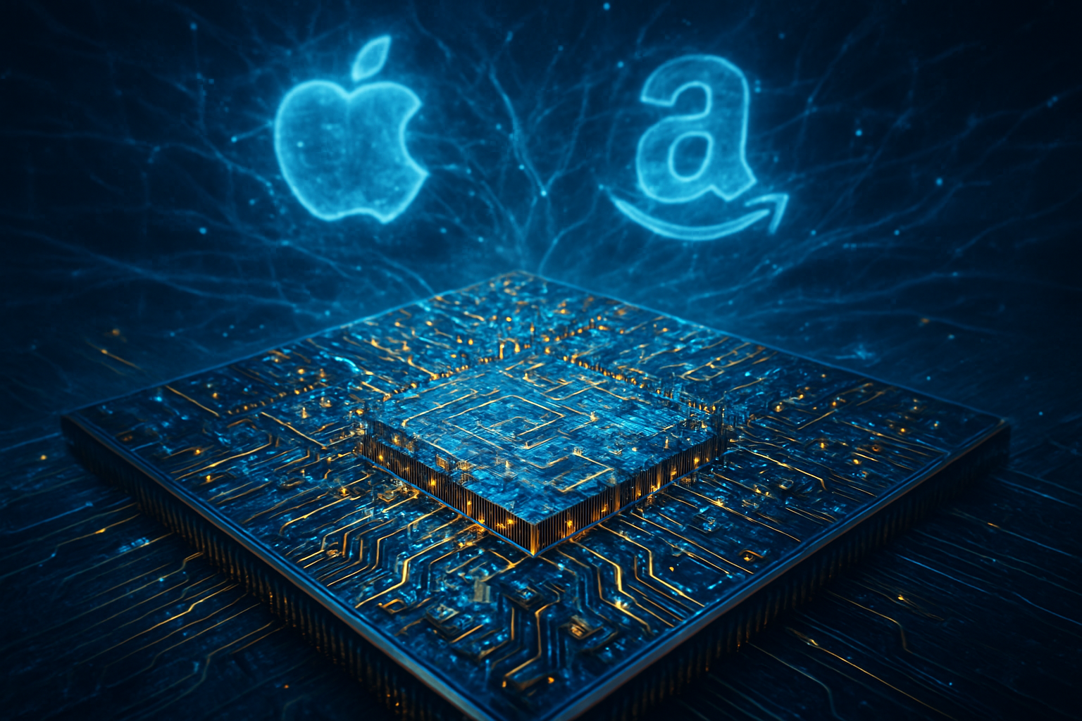
The successful rollout of 18A has immediate and profound implications for the entire semiconductor sector. For years, Advanced Micro Devices (NASDAQ: AMD) and Apple Inc. (NASDAQ: AAPL) enjoyed a manufacturing advantage by leveraging TSMC’s superior nodes. However, with TSMC’s N2 (2nm) process seeing slower-than-expected yields in early 2026, Intel has seized a narrow but critical window of "process leadership." This "leadership" isn't just about Intel’s own chips; it is the cornerstone of the Intel Foundry strategy.
The market impact is already visible. Industry reports indicate that NVIDIA (NASDAQ: NVDA) has committed nearly $5 billion to reserve capacity on Intel’s 18A lines for its next-generation data center components, seeking to diversify its supply chain away from a total reliance on Taiwan. Meanwhile, AMD's upcoming "Zen 6" architecture is not expected to hit the mobile market in volume until late 2026 or early 2027, giving Intel a significant 9-to-12-month head start in the premium laptop and workstation segments.
For startups and smaller AI labs, the proliferation of 180-TOPS consumer hardware lowers the barrier to entry for "Edge AI" applications. Developers can now build sophisticated, privacy-centric AI tools that run entirely on a user's laptop, bypassing the high costs and latency of centralized APIs. This shift threatens the dominance of cloud-only AI providers by moving the "intelligence" back to the local device.
The Geopolitical and Philosophical Significance of 18A
Beyond benchmarks and market share, the 18A milestone is a victory for the "Silicon Shield" strategy in the West. As the first leading-edge node to be manufactured in significant volumes on U.S. soil, 18A represents a critical step toward rebalancing the global semiconductor supply chain. This development fits into the broader trend of "techno-nationalism," where the ability to manufacture the world's fastest transistors is seen as a matter of national security as much as economic prowess.
However, the rapid advancement of local AI capabilities also raises concerns. With Panther Lake making high-performance AI accessible to hundreds of millions of consumers, the industry faces renewed questions regarding deepfakes, local data privacy, and the environmental impact of keeping "AI-always-on" hardware in every home. While Intel claims a record 27 hours of battery life for Panther Lake reference designs, the aggregate energy consumption of an AI-saturated PC market remains a topic of debate among sustainability advocates.
Comparatively, the move to 18A is being likened to the transition from vacuum tubes to integrated circuits. It is a "once-in-a-generation" architectural pivot. While previous nodes focused on incremental shrinks, 18A's combination of backside power and GAA transistors represents a fundamental redesign of how electricity moves through silicon, potentially extending the life of Moore’s Law for another decade.
The Horizon: From Panther Lake to 14A and Beyond
Looking ahead, Intel's roadmap does not stop at 18A. The company is already touting the development of the Intel 14A node, which is expected to integrate High-NA EUV (Extreme Ultraviolet) lithography more extensively. Near-term, the focus will shift from consumer laptops to the data center with "Clearwater Forest," a Xeon processor built on 18A that aims to challenge the dominance of ARM-based server chips in the cloud.
Experts predict that the next two years will see a "Foundry War" as TSMC ramps up its own backside power delivery systems to compete with Intel's early-mover advantage. The primary challenge for Intel now is maintaining these yields as production scales from millions to hundreds of millions of units. Any manufacturing hiccups in the next six months could give rivals an opening to close the gap.
Furthermore, we expect to see a surge in "Physical AI" applications. With Panther Lake being certified for industrial and robotics use cases at launch, the 18A architecture will likely find its way into autonomous delivery drones, medical imaging devices, and advanced manufacturing bots by the end of 2026.
A Turnaround Validated: Final Assessment
The launch of Core Ultra Series 3 at CES 2026 is the ultimate validation of Pat Gelsinger’s "Moonshot" for Intel. By successfully executing five process nodes in four years, the company has transformed itself from a struggling incumbent into a formidable manufacturing powerhouse once again. The 18A node is the physical manifestation of this turnaround—a technological marvel that combines RibbonFET and PowerVia to reclaim the top spot in the semiconductor hierarchy.
Key takeaways for the industry are clear: Intel is no longer "chasing" the leaders; it is setting the pace. The immediate availability of Panther Lake on January 27, 2026, will be the true test of this new era. Watch for the first wave of third-party benchmarks and the subsequent quarterly earnings from Intel and its foundry customers to see if the "18A Era" translates into the financial resurgence the company has promised.
For now, the message from CES is undeniable: the race for the next generation of computing has a new frontrunner, and it is powered by 1.8nm silicon.
This content is intended for informational purposes only and represents analysis of current AI developments.
TokenRing AI delivers enterprise-grade solutions for multi-agent AI workflow orchestration, AI-powered development tools, and seamless remote collaboration platforms.
For more information, visit https://www.tokenring.ai/.