As of January 2026, the global semiconductor landscape has undergone a seismic shift, moving away from the era of "containment" toward a complex new reality of "monetized competition." The geopolitical tug-of-war between the United States and China has solidified into a permanent bifurcation of the technology world, marked by the formalization of the "Pax Silica" alliance—the strategic successor to the "Chip 4" coalition. This new diplomatic framework, which now includes the original Chip 4 nations plus the Netherlands, Singapore, and recent additions like the UAE and Qatar, seeks to insulate the most advanced AI hardware from geopolitical rivals while maintaining a controlled, heavily taxed economic bridge to the East.
The immediate significance of this development cannot be overstated: the U.S. Department of Commerce has officially pivoted from a blanket "presumption of denial" for high-end chip exports to a "case-by-case review" system paired with a mandatory 25% "chip tax" on all advanced AI silicon bound for China. This policy allows Western titans like NVIDIA (NASDAQ:NVDA) to maintain market share while simultaneously generating billions in revenue for the U.S. government to reinvest in domestic sub-2nm fabrication and research. However, this bridge comes with strings attached, as the most cutting-edge "sovereign-grade" AI architectures remain strictly off-limits to any nation outside the Pax Silica security umbrella.
The Architecture of Exclusion: GAA Transistors and HBM Chokepoints
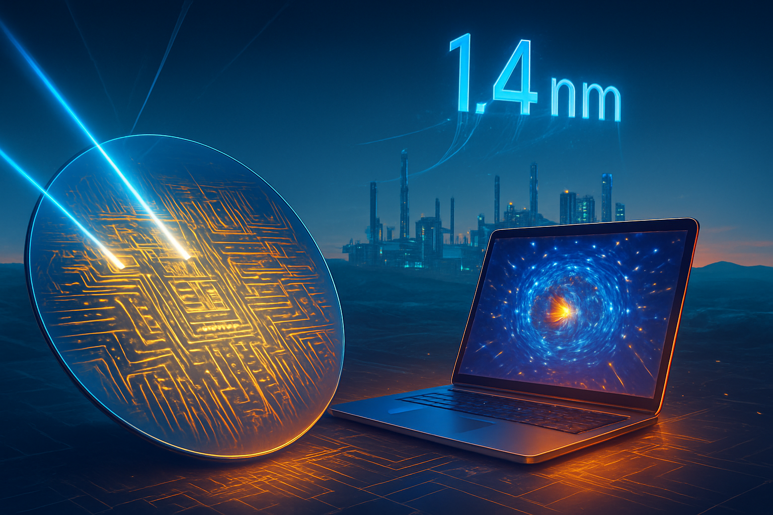
Technically, the new trade restrictions center on two critical pillars of next-generation computing: Gate-All-Around (GAA) transistor technology and High Bandwidth Memory (HBM). While the previous decade was defined by FinFET transistors, the leap to 2nm and 3nm nodes requires the adoption of GAA, which allows for finer control over current and significantly lower power consumption—essential for the massive energy demands of 2026-era Large Action Models (LAMs). New export rules, specifically ECCN 3A090.c, now strictly control the software, recipes, and hybrid bonding tools required to manufacture GAA-based chips, effectively stalling China’s progress at the 5nm ceiling.
In the memory sector, HBM has become the "new oil" of the AI industry. The Pax Silica alliance has placed a firm stranglehold on the specialized stacking and bonding equipment required to produce HBM4, the current industry standard. This has forced Chinese firms like SMIC (HKG:0981) to attempt to localize the entire HBM supply chain—a monumental task that experts suggest is at least three to five years behind the state-of-the-art. Industry analysts note that while SMIC has managed to produce 5nm-class chips using older Deep Ultraviolet (DUV) lithography, their yields are reportedly hovering around a disastrous 33%, making their domestic AI accelerators nearly twice as expensive as their Western counterparts.
Initial reactions from the AI research community have been polarized. While some argue that these restrictions prevent the proliferation of dual-use AI for military applications, others fear a "hardware apartheid" that could slow global scientific progress. The shift by ASML (NASDAQ:ASML) to fully align with U.S. policy, halting the export of even high-end immersion DUV tools to China, has further tightened the noose, forcing Chinese researchers to focus on algorithmic efficiency and "compute-light" AI models to compensate for their lack of raw hardware power.
A Two-Tiered Market: Winners and Losers in the New Trade Regime
For the corporate giants of Silicon Valley and East Asia, 2026 is a year of navigating "dual-track" product lines. NVIDIA (NASDAQ:NVDA) recently unveiled its "Rubin" platform, a successor to the Blackwell architecture featuring Vera CPUs. Crucially, the Rubin platform is classified as "Pax Silica Only," meaning it cannot be exported to China even with the 25% tax. Instead, NVIDIA is shipping the older H200 and specialized "H20" variants to the Chinese market, subject to a volume cap that prevents China-bound shipments from exceeding 50% of U.S. domestic sales. This strategy allows NVIDIA to keep its dominant position in the Chinese enterprise market while ensuring the U.S. maintains a "two-generation lead."
The strategic positioning of TSMC (NYSE:TSM) has also evolved. Through a landmark $250 billion "Silicon Shield" agreement finalized in early 2026, TSMC has secured massive federal subsidies for its Arizona and Dresden facilities in exchange for prioritizing Pax Silica defense and AI infrastructure needs. This has mitigated fears of a "hollowing out" of Taiwan’s industrial base, as the island remains the exclusive home for the initial "N2" (2nm) mass production. Meanwhile, South Korean giants Samsung (KRX:005930) and SK Hynix (KRX:000660) are reaping the benefits of the HBM shortage, though they face the difficult task of phasing out their legacy manufacturing footprints in mainland China to comply with the new alliance standards.
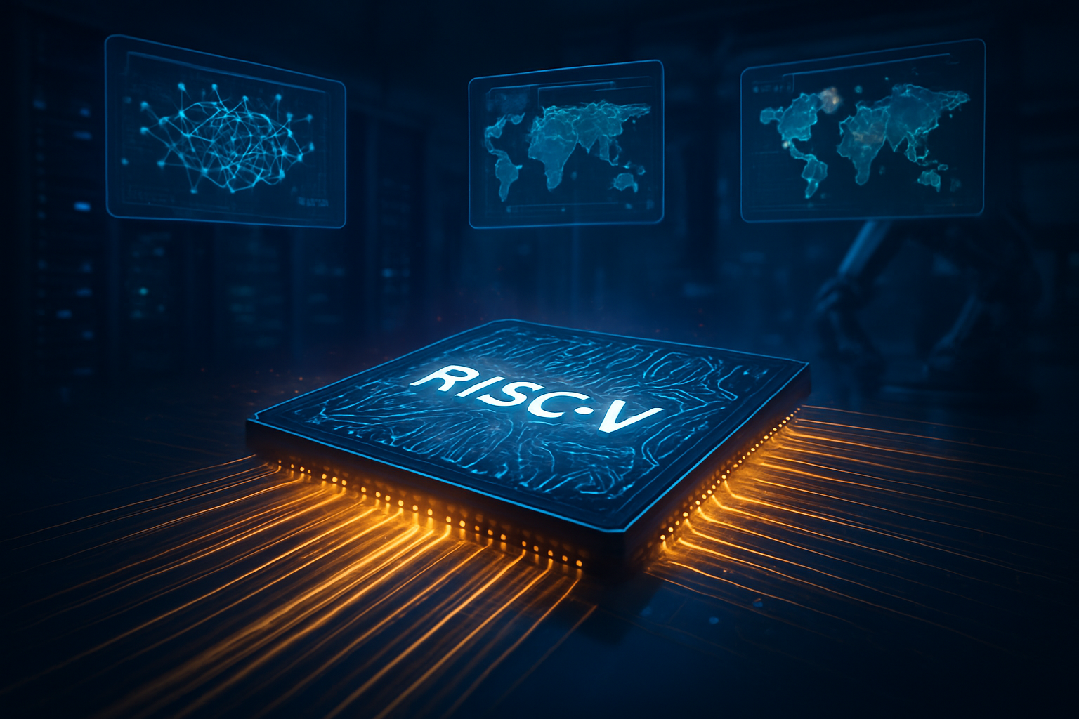
Startups in the AI space are feeling the squeeze of this bifurcation. New ventures in India and Singapore are benefiting from being inside the Pax Silica "trusted circle," gaining access to advanced compute that was previously reserved for U.S. and European firms. Conversely, Chinese AI startups are pivoting toward RISC-V architectures and domestic accelerators, creating a siloed ecosystem that is increasingly incompatible with Western software stacks like CUDA, potentially leading to a permanent divergence in AI development environments.
The Geopolitical Gamble: Sovereignty vs. Globalization
The wider significance of these trade restrictions marks the end of the "Global Village" era for high-technology. We are witnessing the birth of "Semiconductor Sovereignty," where the ability to design and manufacture silicon is viewed as being as vital to national security as a nuclear deterrent. This fits into a broader trend of "de-risking" rather than "de-coupling," where the U.S. and its allies seek to control the heights of the AI revolution while maintaining enough trade to prevent a total economic collapse.
The Pax Silica alliance represents a sophisticated evolution of the Cold War-era COCOM (Coordinating Committee for Multilateral Export Controls). By including energy-rich nations like the UAE and Qatar, the U.S. is effectively trading access to high-end AI chips for long-term energy security and a commitment to Western data standards. However, this creates a potential "splinternet" of hardware, where the world is divided into those who can run 2026’s most advanced models and those who are stuck with the "legacy" AI of 2024.
Comparisons to previous milestones, such as the 1986 U.S.-Japan Semiconductor Agreement, highlight the increased stakes. In the 1980s, the battle was over memory chips for PCs; today, it is over the foundational "intelligence" that will power autonomous economies, defense systems, and scientific discovery. The concern remains that by pushing China into a corner, the West is incentivizing a radical, independent breakthrough in areas like optical computing or carbon nanotube transistors—technologies that could eventually bypass the silicon-based chokepoints currently being exploited.
The Horizon: Photonics, RISC-V, and the 2028 Deadline
Looking ahead, the next 24 months will be a race against time. China has set a national goal for 2028 to achieve "EUV-equivalence" through alternative lithography techniques and advanced chiplet packaging. While Western experts remain skeptical, the massive influx of capital into China’s "Big Fund Phase 3" is accelerating the localization of ion implanters and etching equipment. We can expect to see the first "all-Chinese" 7nm AI chips hitting the market by late 2026, though their performance per watt will likely lag behind the West’s 2nm offerings.
In the near term, the industry is closely watching the development of silicon photonics. This technology, which uses light instead of electricity to move data between chips, could be the key to overcoming the interconnect bottlenecks that currently plague AI clusters. Because photonics relies on different manufacturing processes than traditional logic chips, it could become a new "gray zone" for trade restrictions, as the Pax Silica framework struggles to categorize these hybrid devices.
The long-term challenge will be the "talent drain." As the hardware divide grows, we may see a migration of researchers toward whichever ecosystem provides the best "compute-to-cost" ratio. If China can subsidize its inefficient 5nm chips enough to make them accessible to global researchers, it could create a gravity well for AI development that rivals the Western hubs, despite the technical inferiority of the underlying hardware.
A New Equilibrium in the AI Era
The geopolitical hardening of the semiconductor supply chain in early 2026 represents a definitive closing of the frontier. The transition from the "Chip 4" to "Pax Silica" and the implementation of the 25% "chip tax" signals that the U.S. has accepted the permanence of its rivalry with China and has moved to monetize it while protecting its technological lead. This development will be remembered as the moment the AI revolution was formally subsumed by the machinery of statecraft.
Key takeaways for the coming months include the performance of NVIDIA's Rubin platform within the Pax Silica bloc and whether China can successfully scale its 5nm "inefficiency-node" production to meet domestic demand. The "Silicon Shield" around Taiwan appears stronger than ever, but the cost of that security is a more expensive, more fragmented global market.
In the weeks ahead, watch for the first quarterly reports from ASML (NASDAQ:ASML) and TSMC (NYSE:TSM) to see the true impact of the Dutch export bans and the U.S. investment deals. As the "Silicon Iron Curtain" descends, the primary question remains: will this enforced lead protect Western interests, or will it merely accelerate the arrival of a competitor that the West no longer understands?
This content is intended for informational purposes only and represents analysis of current AI developments.
TokenRing AI delivers enterprise-grade solutions for multi-agent AI workflow orchestration, AI-powered development tools, and seamless remote collaboration platforms.
For more information, visit https://www.tokenring.ai/.