In a move that signals a seismic shift in the semiconductor industry, GlobalFoundries (Nasdaq: GFS) announced on January 14, 2026, a definitive agreement to acquire the Processor IP Solutions business from Synopsys (Nasdaq: SNPS). This strategic acquisition, following GlobalFoundries’ 2025 purchase of MIPS, marks the company’s transition from a traditional "pure-play" contract manufacturer into a vertically integrated powerhouse capable of providing end-to-end custom silicon solutions. By absorbing one of the industry's most successful processor portfolios, GlobalFoundries is positioning itself as the primary architect for the next generation of "Physical AI"—the intelligence embedded in machines that interact with the physical world.
The immediate significance of this deal cannot be overstated. As the semiconductor world pivots from the cloud-centric "Digital AI" era toward an "Edge AI" supercycle, the demand for specialized, power-efficient chips has skyrocketed. By owning the underlying processor architecture, development tools, and manufacturing processes, GlobalFoundries can now offer customers a streamlined path to custom silicon, bypassing the high licensing fees and generic constraints of traditional third-party IP providers. This move effectively "commoditizes the complement" for GlobalFoundries' manufacturing business, providing a compelling reason for chip designers to choose GF’s specialized manufacturing nodes over larger rivals.
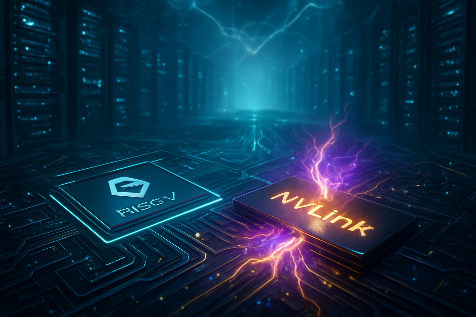
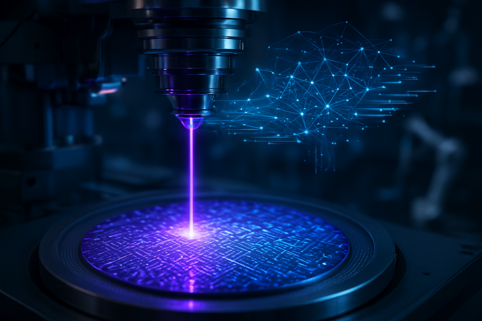
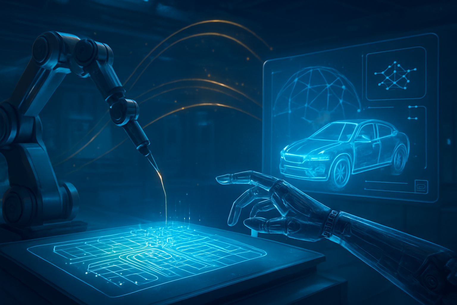
The Technical Edge: ARC-V and the Shift to Custom Silicon
The acquisition encompasses Synopsys’ entire ARC processor portfolio, including the highly anticipated ARC-V family based on the open-source RISC-V instruction set architecture. Beyond general-purpose CPUs, the deal includes critical AI-enablement components: the VPX Digital Signal Processors (DSP) for high-performance audio and sensing, and the NPX Neural Processing Units (NPU) for hardware-accelerated machine learning. Crucially, GlobalFoundries also gains control of the ARC MetaWare development toolset and the ASIP (Application-Specific Instruction-set Processor) Designer tool. This software suite allows customers to tailor their own instruction sets, creating chips that are mathematically optimized for specific tasks—such as 3D spatial mapping in robotics or real-time sensor fusion in autonomous vehicles.
This approach differs radically from the traditional foundry-customer relationship. Previously, a chip designer would license IP from a company like Arm (Nasdaq: ARM) or Cadence (Nasdaq: CDNS) and then shop for a manufacturer. GlobalFoundries is now offering a "pre-optimized" ecosystem where the IP is tuned specifically for its own manufacturing processes, such as its 22FDX (FD-SOI) technology. This vertical integration reduces the "power-performance-area" (PPA) trade-offs that often plague general-purpose designs. The industry reaction has been swift, with technical experts noting that the integration of the ASIP Designer tool under a foundry roof is a "game changer" for companies needing to build bespoke hardware for niche AI workloads that don't fit the cookie-cutter templates of the past.
Disrupting the Status Quo: Strategic Advantages and Market Positioning
The acquisition places GlobalFoundries in direct competition with its long-term IP partners, most notably Arm. While Arm remains the dominant force in mobile and data center markets, its business model is inherently foundry-neutral. By bundling IP with manufacturing, GlobalFoundries can offer a "royalty-free" or significantly discounted licensing model for customers who commit to their fabrication plants. This is particularly attractive for high-volume, cost-sensitive markets like wearables and IoT sensors, where every cent of royalty can impact the bottom line. Startups and automotive Tier-1 suppliers are expected to be the primary beneficiaries, as they can now access high-end processor IP and a manufacturing path through a single point of contact.
For Synopsys (Nasdaq: SNPS), the sale represents a strategic pivot. Following its massive $35 billion acquisition of Ansys, Synopsys is refocusing its efforts on "Interface and Foundation IP"—the high-speed connectors like PCIe, DDR, and UCIe that allow different chips to talk to each other in complex "chiplet" designs. By divesting its processor business to GlobalFoundries, Synopsys exits a market where it was increasingly competing with its own customers, such as Arm and other RISC-V startups. This allows Synopsys to double down on its "Silicon to Systems" strategy, providing the EDA tools and interface standards that the entire industry relies on, regardless of which processor architecture wins the market.
The Era of Physical AI and Silicon Sovereignty
The timing of this acquisition aligns with the "Physical AI" trend that dominated the tech landscape in early 2026. Unlike the Generative AI of previous years, which focused on language and images in the cloud, Physical AI refers to intelligence embedded in hardware that senses, reasons, and acts in real-time. GlobalFoundries is betting that the most valuable silicon in the next decade will be found in humanoid robots, industrial drones, and sophisticated medical devices. These applications require ultra-low latency and extreme power efficiency, which are best achieved through the custom, event-driven computing architectures found in the ARC and MIPS portfolios.
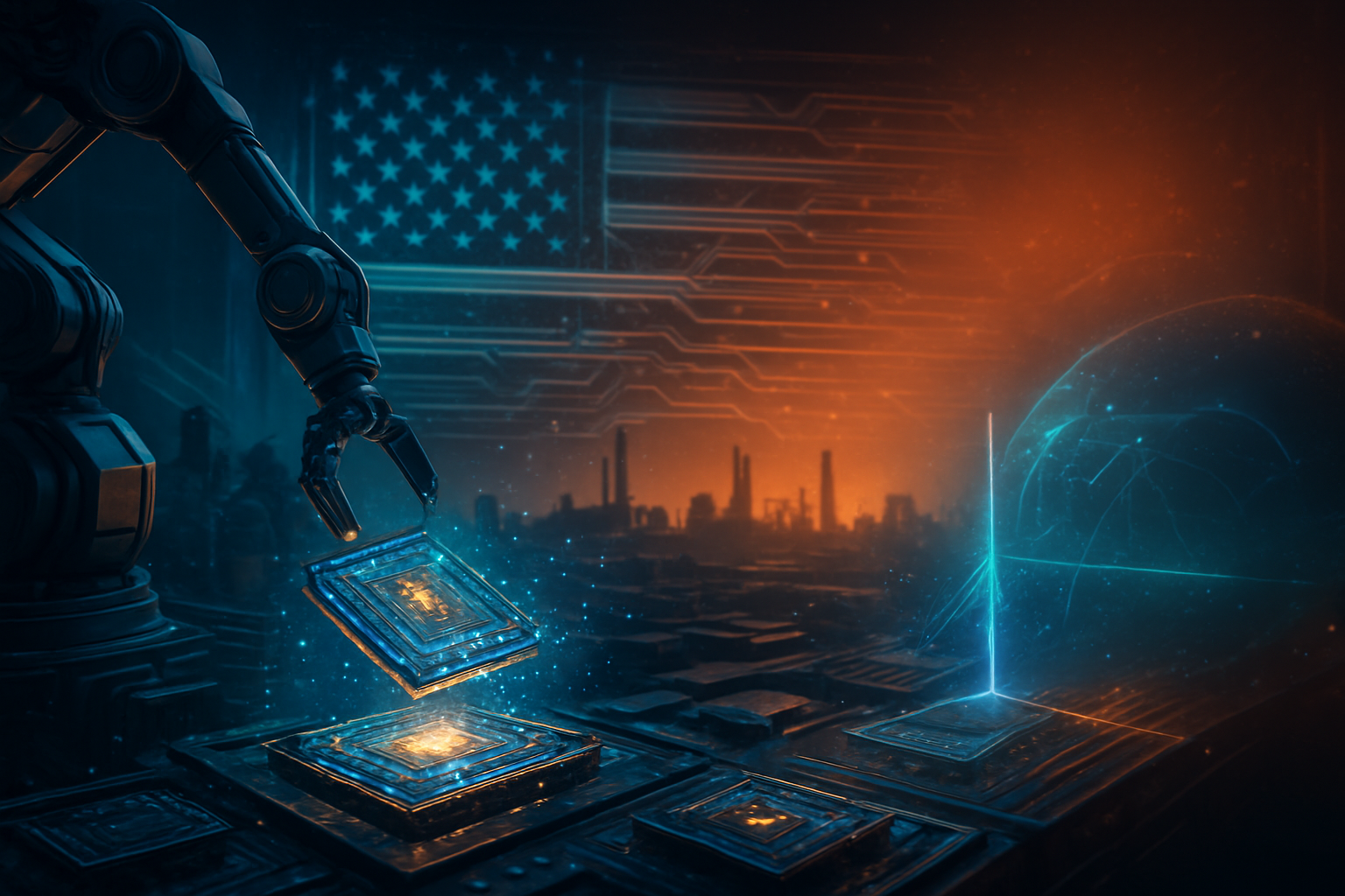
Furthermore, this deal addresses the growing global demand for "silicon sovereignty." As nations seek to secure their technology supply chains, GlobalFoundries—the only major foundry with a significant manufacturing footprint across the U.S. and Europe—now offers a more complete, secure domestic solution. By providing the architecture, the tools, and the manufacturing within a trusted ecosystem, GF is appealing to government and defense sectors that are wary of the geopolitical risks associated with fragmented supply chains and proprietary foreign IP.
Looking Ahead: The Road to MIPS Integration and Autonomous Machines
In the near term, GlobalFoundries plans to integrate the acquired Synopsys assets into its MIPS subsidiary, creating a unified processor division. This synergy will likely produce a new class of hybrid processors that combine MIPS' expertise in automotive-grade safety and multithreading with ARC’s configurable AI acceleration. We can expect to see the first "GF-Certified" reference designs for automotive ADAS (Advanced Driver Assistance Systems) and collaborative industrial robots hit the market by the end of 2026. These platforms will allow manufacturers to deploy AI at the edge with significantly lower power consumption than current GPU-based solutions.
However, challenges remain. The integration of two distinct processor architectures—ARC and MIPS—will require a massive software consolidation effort to ensure a seamless experience for developers. Furthermore, while RISC-V (via ARC-V) offers a flexible path forward, the ecosystem is still maturing compared to Arm’s well-established developer base. Experts predict that GlobalFoundries will need to invest heavily in the open-source community to ensure that its custom silicon solutions have the necessary software support to compete with the industry giants.
A New Chapter in Semiconductor History
GlobalFoundries’ acquisition of Synopsys’ Processor IP Solutions is a watershed moment that redraws the boundaries between chip design and manufacturing. By vertically integrating the ARC and RISC-V portfolios, GF is moving beyond its role as a silent partner in the semiconductor industry to become a leading protagonist in the Physical AI revolution. The deal effectively creates a "one-stop shop" for custom silicon, challenging the dominance of established IP providers and offering a more efficient, sovereign-friendly path for the next generation of intelligent machines.
As the transaction moves toward its expected close in the second half of 2026, the industry will be watching closely to see how GlobalFoundries leverages its newfound architectural muscle. The successful integration of these assets could trigger a wave of similar consolidations, as other foundries realize that in the age of AI, owning the "brains" of the chip is just as important as owning the factory that builds it. For now, GlobalFoundries has positioned itself at the vanguard of a new era where silicon and software are inextricably linked, paving the way for a world where intelligence is embedded in every physical object.
This content is intended for informational purposes only and represents analysis of current AI developments.
TokenRing AI delivers enterprise-grade solutions for multi-agent AI workflow orchestration, AI-powered development tools, and seamless remote collaboration platforms.
For more information, visit https://www.tokenring.ai/.