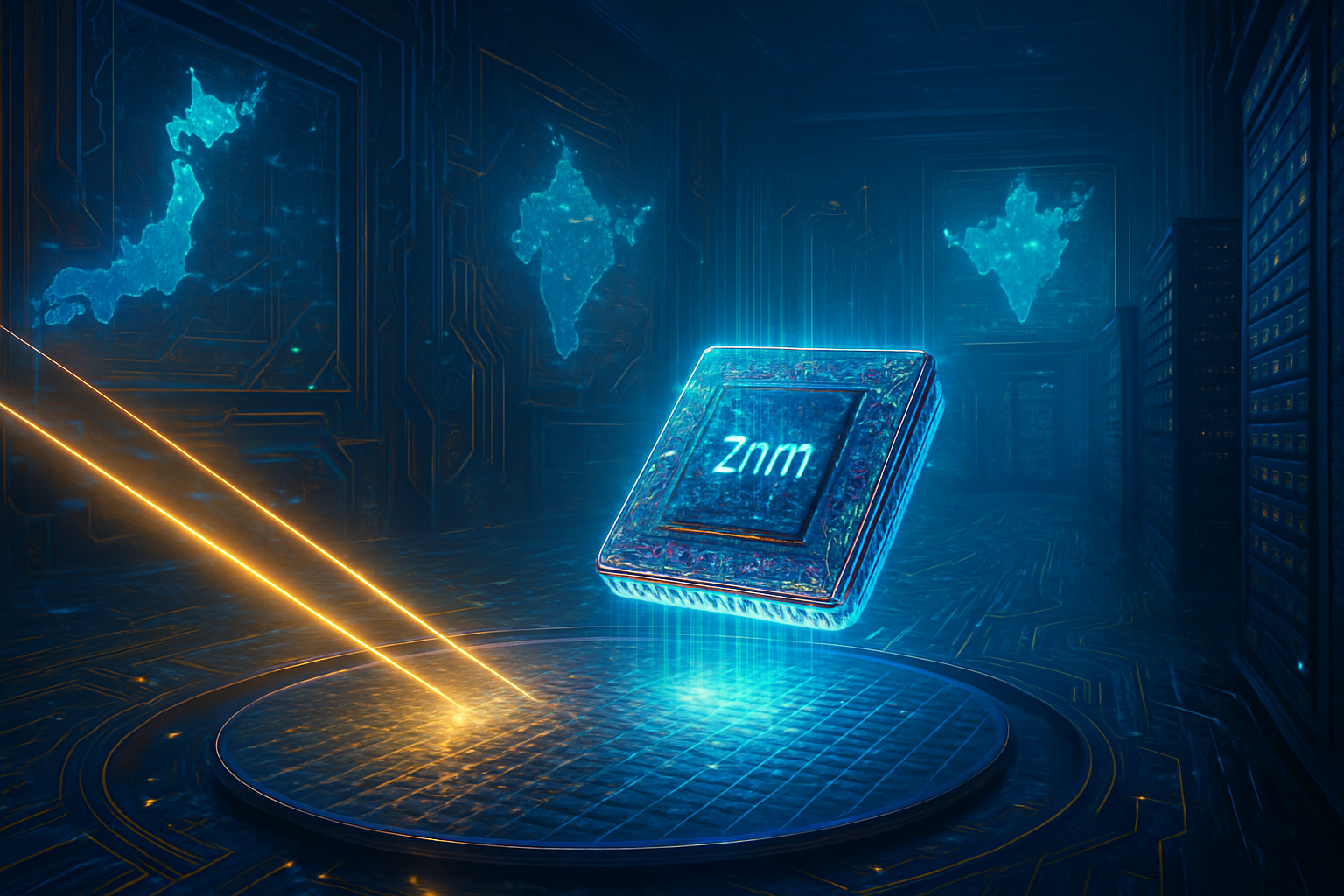
The semiconductor industry has reached a historic inflection point in January 2026, as the "Great Flip" from front-side to backside power delivery becomes the defining standard for the sub-2nm era. At the heart of this architectural shift is Intel Corporation (NASDAQ: INTC) and its proprietary PowerVia technology. By moving a chip’s power delivery network to the "backside" of the silicon wafer, Intel has effectively decoupled power and signaling—a move that industry experts describe as the most significant change to transistor architecture since the introduction of FinFET over a decade ago.
As of early 2026, the success of the Intel 18A node has validated this risky bet. By being the first to commercialize backside power delivery (BSPD) in high-volume manufacturing, Intel has not only hit its ambitious "five nodes in four years" target but has also provided a critical lifeline for the AI industry. With high-end AI accelerators now pushing toward 1,000-watt power envelopes, traditional front-side wiring had hit a "power wall" where electrical resistance and congestion were stalling performance gains. PowerVia has shattered this wall, enabling the massive transistor densities and energy efficiencies required for the next generation of trillion-parameter large language models (LLMs).
The Engineering Behind the 'Great Flip'
The technical genius of PowerVia lies in how it addresses IR drop—the phenomenon where voltage decreases as it travels through a chip’s complex internal wiring. In traditional designs, both power and data signals compete for space in a "spaghetti" of metal layers stacked on top of the transistors. As transistors shrink toward 2nm and beyond, these wires become so thin and crowded that they generate excessive heat and lose significant voltage before reaching their destination. PowerVia solves this by relocating the entire power grid to the underside of the silicon wafer.
This architecture utilizes Nano-TSVs (Through-Silicon Vias), which are roughly 500 times smaller than standard TSVs, to connect the backside power rails directly to the transistors. According to results from Intel’s Blue Sky Creek test chip, this method reduces platform voltage droop by a staggering 30% and allows for more than 90% cell utilization. By removing the bulky power wires from the front side, engineers can now use "relaxed" wiring for signals, reducing interference and allowing for a 6% boost in clock frequencies without any changes to the underlying transistor design.
This shift represents a fundamental departure from the manufacturing processes used by Taiwan Semiconductor Manufacturing Company (NYSE: TSM) and Samsung Electronics (KRX: 005930) in their previous 3nm and early 2nm nodes. While competitors have relied on optimizing the existing front-side stack, Intel’s decision to move to the backside required mastering a complex process of wafer flipping, thinning the silicon to a few micrometers, and achieving nanometer-scale alignment for the Nano-TSVs. The successful yields reported this month on the 18A node suggest that Intel has solved the structural integrity and alignment issues that many feared would delay the technology.
A New Competitive Paradigm for Foundries
The commercialization of PowerVia has fundamentally altered the competitive landscape of the semiconductor market in 2026. Intel currently holds a 1.5-to-2-year "first-mover" advantage over TSMC, whose equivalent technology, the A16 Super Power Rail, is only now entering risk production. This lead has allowed Intel Foundry Services (IFS) to secure massive contracts from tech giants looking to diversify their supply chains. Microsoft Corporation (NASDAQ: MSFT) has become a flagship customer, utilizing the 18A node for its Maia 2 AI accelerator to manage the intense power requirements of its Azure AI infrastructure.
Perhaps the most significant market shift is the strategic pivot by NVIDIA Corporation (NASDAQ: NVDA). While NVIDIA continues to rely on TSMC for its highest-end GPU production, it recently finalized a $5 billion co-development deal with Intel to leverage PowerVia and advanced Foveros packaging for next-generation server CPUs. This multi-foundry approach highlights a new reality: in 2026, manufacturing location and architectural efficiency are as important as pure transistor size. Intel’s ability to offer a "National Champion" manufacturing base on U.S. soil, combined with its lead in backside power, has made it a credible alternative to TSMC for the world's most demanding AI silicon.
Samsung Electronics is also in the fray, attempting to leapfrog the industry by pulling forward its SF2Z node, which integrates its own version of backside power. However, as of January 2026, Intel’s high-volume manufacturing (HVM) status gives it the upper hand in "de-risking" the technology for risk-averse chip designers. Electronic Design Automation (EDA) leaders like Synopsys (NASDAQ: SNPS) and Cadence Design Systems (NASDAQ: CDNS) have already integrated PowerVia-specific tools into their suites, further cementing Intel’s architectural lead in the design ecosystem.
Breaking the AI Thermal Ceiling
The wider significance of PowerVia extends beyond mere manufacturing specs; it is a critical enabler for the future of AI. As AI models become more "agentic" and complex, the chips powering them have faced an escalating thermal crisis. By thinning the silicon wafer to accommodate backside power, manufacturers have inadvertently created a more efficient thermal path. The heat-generating transistors are now physically closer to the cooling solutions on the back of the chip, making advanced liquid-cooling and microfluidic integration much more effective.
This architectural shift has also allowed for a massive increase in logic density. By "de-cluttering" the front side of the chip, manufacturers can pack more specialized Neural Processing Units (NPUs) and larger SRAM caches into the same physical footprint. For AI researchers, this translates to chips that can handle more parameters on-device, reducing the latency for real-time AI applications. The 30% area reduction offered by the 18A node means that the 2026 generation of smartphones and laptops can run sophisticated LLMs that previously required data center connectivity.
However, the transition has not been without concerns. The extreme precision required to bond and thin wafers has led to higher initial costs, widening the "compute divide" between well-funded tech giants and smaller startups. Furthermore, the concentration of power on the backside creates intense localized "hot spots" that require a new generation of cooling technologies, such as diamond-based heat spreaders. Despite these challenges, the consensus among the AI research community is that PowerVia was the necessary price of admission for the Angstrom era of computing.
The Road to Sub-1nm and Beyond
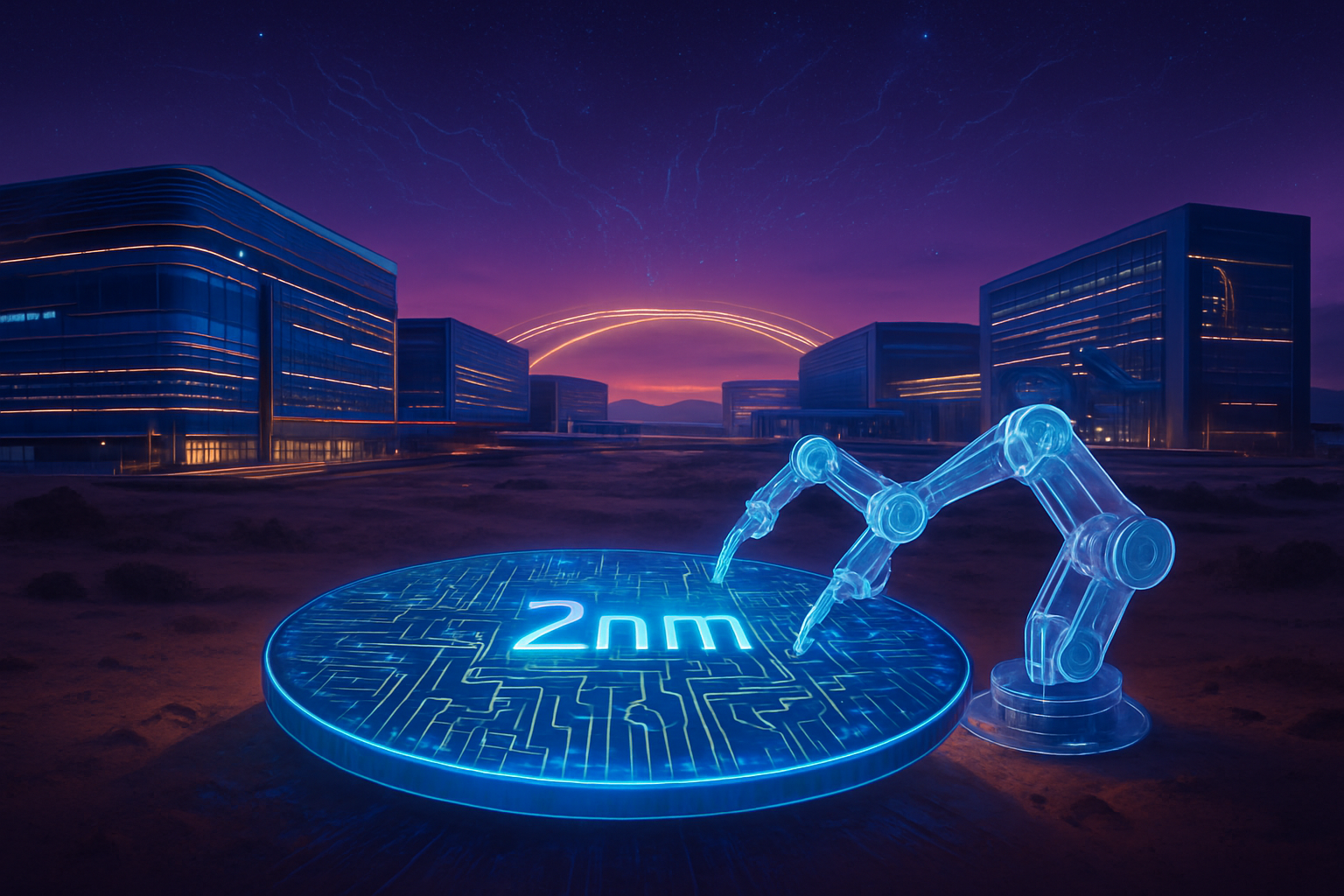
Looking ahead, the success of PowerVia is just the first step in a broader roadmap toward three-dimensional vertical stacking. Intel is already sharing design kits for its 14A node, which will introduce PowerDirect—a second-generation backside technology that connects power directly to the source and drain of the transistor, further reducing resistance. Experts predict that by 2028, the industry will move toward "backside signaling," where non-critical data paths are also moved to the back, leaving the front side exclusively for high-speed logic and optical interconnects.
The next major milestone to watch is the integration of PowerVia with High-NA EUV (Extreme Ultraviolet) lithography. This combination will allow for even finer transistor features and is expected to be the foundation for the 10A node later this decade. Challenges remain in maintaining high yields as the silicon becomes thinner and more fragile, but the industry's rapid adoption of backside-aware EDA tools suggests that the design hurdles are being cleared faster than anticipated.
A Legacy of Innovation in the AI Era
In summary, Intel’s PowerVia represents one of the most successful "comeback" stories in the history of silicon manufacturing. By identifying the power delivery bottleneck early and committing to a radical architectural change, Intel has reclaimed its position as a technical pioneer. The successful ramp-up of the 18A node in early 2026 marks the end of the "spaghetti" era of chip design and the beginning of a new 3D paradigm that treats both sides of the wafer as active real estate.
For the tech industry, the implications are clear: the power wall has been breached. As we move further into 2026, the focus will shift from whether backside power works to how quickly it can be scaled across all segments of computing. Investors and analysts should keep a close eye on the performance of Intel’s "Panther Lake" and "Clearwater Forest" chips in the coming months, as these will be the ultimate barometers for PowerVia’s impact on the global AI economy.
This content is intended for informational purposes only and represents analysis of current AI developments.
TokenRing AI delivers enterprise-grade solutions for multi-agent AI workflow orchestration, AI-powered development tools, and seamless remote collaboration platforms.
For more information, visit https://www.tokenring.ai/.