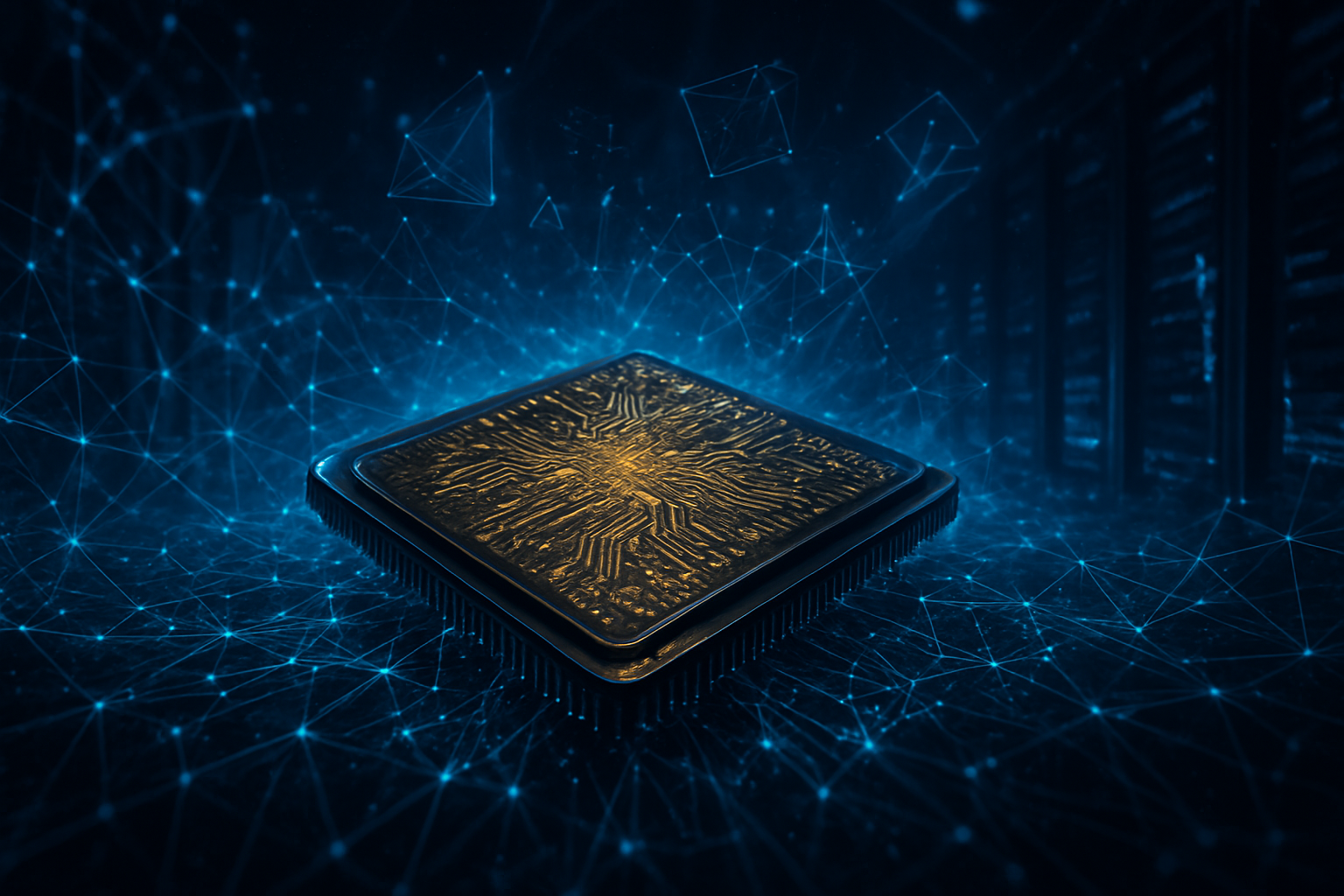
In a milestone that signals a definitive shift in the global semiconductor balance of power, the China Institute of Atomic Energy (CIAE) announced on January 12, 2026, the successful beam extraction and performance validation of the POWER-750H, China’s first domestically developed tandem-type high-energy hydrogen ion implanter. This development represents the completion of the "final piece" in China’s domestic chipmaking puzzle, closing the technology gap in one of the few remaining "bottleneck" areas where the country was previously 100% dependent on imports from US and Japanese vendors.
The immediate significance of the POWER-750H cannot be overstated. High-energy ion implantation is a critical process for manufacturing the specialized power semiconductors and image sensors that drive modern AI data centers and electric vehicles. By mastering this technology amidst intensifying trade restrictions, China has effectively neutralized a key lever of Western export controls, securing the foundational equipment needed to scale its internal AI infrastructure and power electronics industry without fear of further technological decapitation.
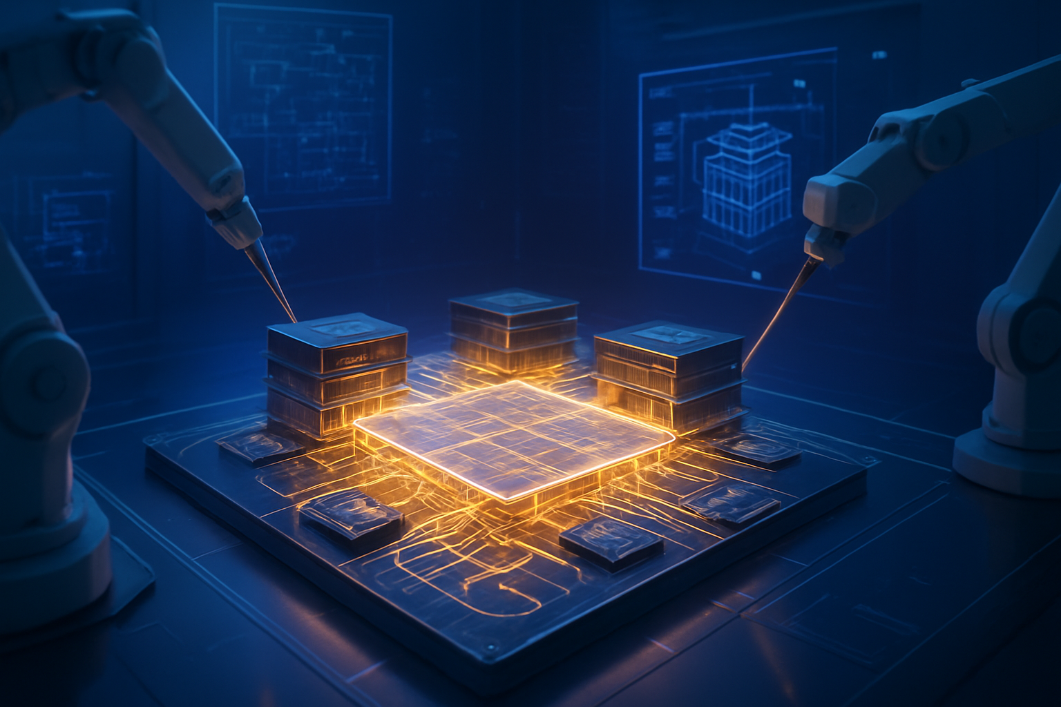
Technical Mastery: The Power of Tandem Acceleration
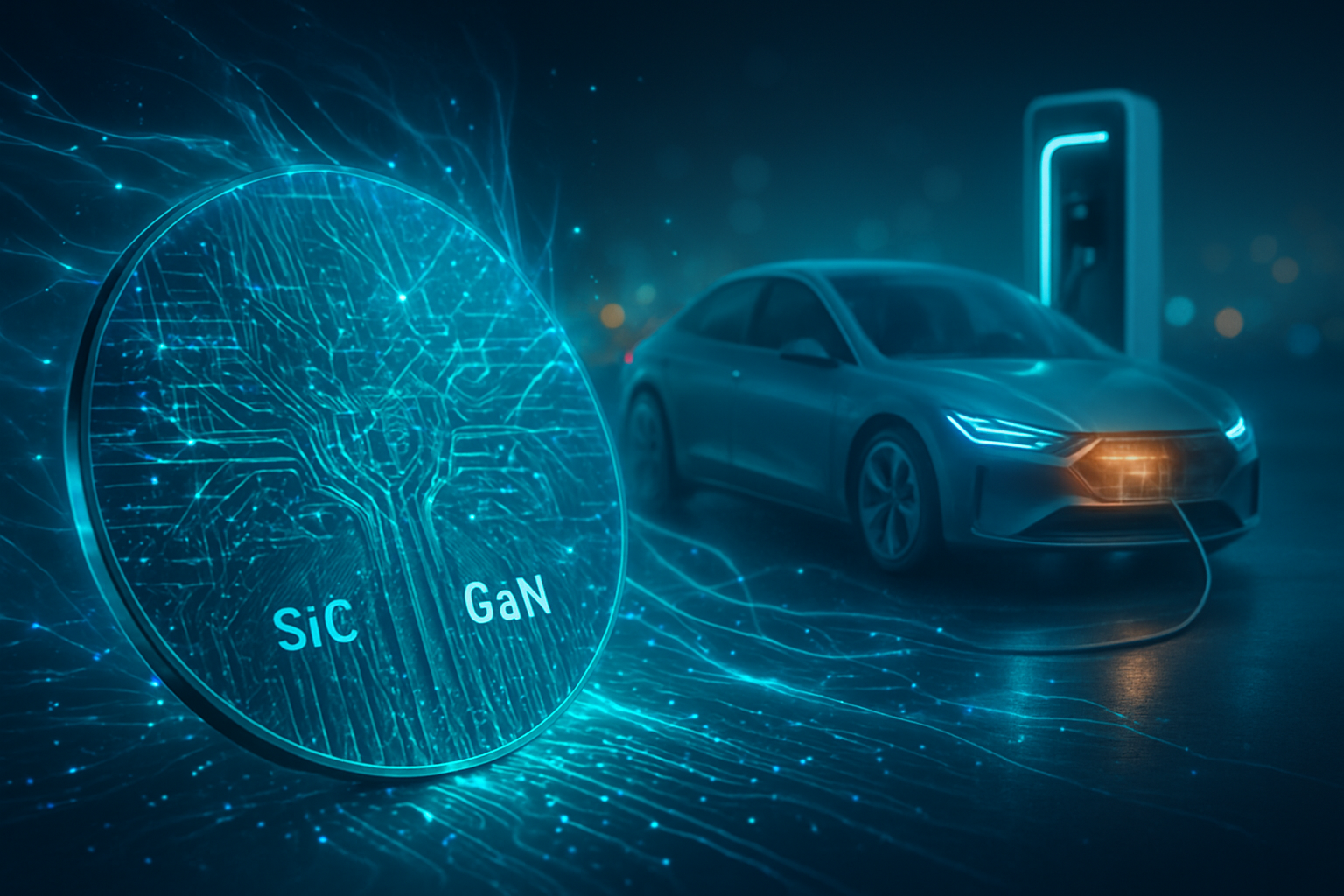
The POWER-750H is not merely an incremental improvement but a fundamental leap in domestic precision engineering. Unlike standard medium-current implanters, high-energy systems must accelerate ions to mega-electron volt (MeV) levels to penetrate deep into silicon wafers. The "750" in its designation refers to its 750kV high-voltage terminal, which, through tandem acceleration, allows it to generate ion beams with effective energies exceeding 1.5 MeV. This technical capability is essential for "deep junction" doping—a process required to create the robust transistors found in high-voltage power management ICs (PMICs) and high-density memory.
Technically, the POWER-750H differs from previous Chinese attempts by utilizing a tandem accelerator architecture, which uses a single high-voltage terminal to accelerate ions twice, significantly increasing energy efficiency and beam stability within a smaller footprint. This approach mirrors the advanced systems produced by industry leaders like Axcelis Technologies (NASDAQ: ACLS), yet it has been optimized for the specific "profile engineering" required for wide-bandgap semiconductors like Silicon Carbide (SiC) and Gallium Nitride (GaN). Initial reactions from the domestic research community suggest that the POWER-750H achieves a beam purity and dose uniformity that rivals the venerable Purion series from Axcelis, marking a transition from laboratory prototype to industrial-grade tool.
Market Seismic Shifts: SMIC, Wanye, and the Retreat of the Giants
The commercialization of these tools is already reshaping the financial landscape of the semiconductor industry. SMIC (HKG: 0981), China’s largest foundry, has reportedly recalibrated its 2026 capital expenditure (CAPEX) strategy, allocating over 70% of its equipment budget to domestic vendors. This "national team" pivot has provided a massive tailwind for Wanye Enterprises (SHA: 600641), whose subsidiary, Kingsemi, has moved into mass deployment of high-energy models. Market analysts predict that Wanye will capture nearly 40% of the domestic ion implanter market share by the end of 2026, a space that was once an uncontested monopoly for Western firms.
Conversely, the impact on US equipment giants has been severe. Applied Materials (NASDAQ: AMAT), which historically derived a significant portion of its revenue from the Chinese market, has seen its China-based sales guidance drop from 40% to approximately 25% for the 2026 fiscal year. Even more dramatic was the late-2025 defensive merger between Axcelis and Veeco Instruments (NASDAQ: VECO), a move widely interpreted as an attempt to diversify away from a pure-play ion implantation focus as Chinese domestic alternatives began to saturate the power semiconductor market. The loss of the Chinese "legacy node" and power-chip markets has forced these companies to pivot aggressively toward advanced packaging and High Bandwidth Memory (HBM) tools in the US and South Korea to sustain growth.
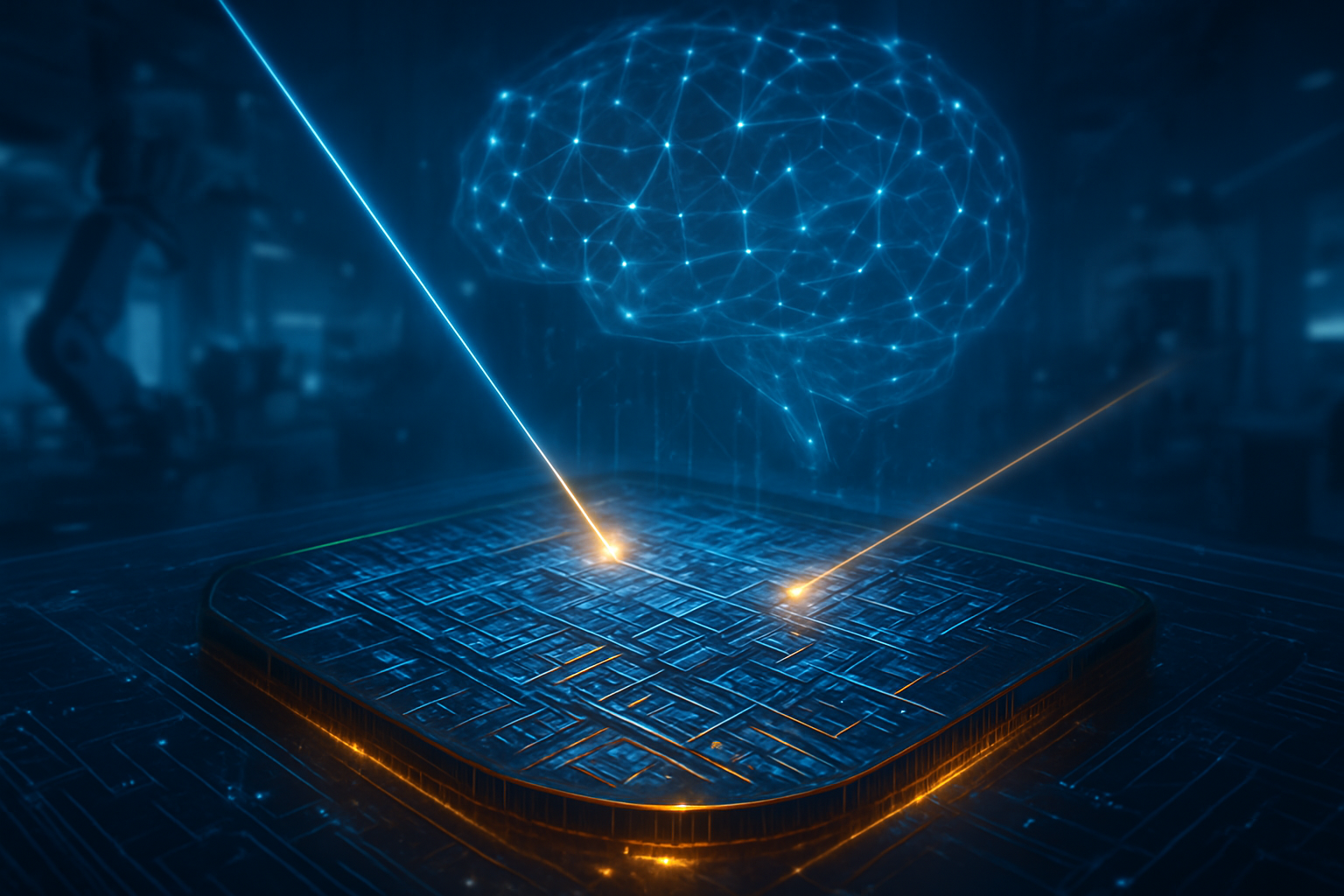
The AI Connection: Powering the Factories of the Future
Beyond the fabrication of logic chips, the significance of high-energy ion implantation lies in its role in the "AI infrastructure supercycle." Modern AI data centers, which are projected to consume massive amounts of power by the end of 2026, rely on high-efficiency power management systems to operate. Domestic high-energy implanters allow China to produce the specialized MOSFETs and IGBTs needed for these data centers internally. This ensures that China's push for "AI Sovereignty"—the ability to train and run massive large language models on an entirely domestic hardware stack—remains on track.
This milestone is a pivotal moment in the broader trend of global "de-globalization" in tech. Just as the US has sought to restrict China’s access to 3nm and 5nm lithography, China has responded by achieving self-sufficiency in the tools required for the "power backbone" of AI. This mirrors previous breakthroughs in etching and thin-film deposition, signaling that the era of using semiconductor equipment as a geopolitical weapon may be reaching a point of diminishing returns. The primary concern among international observers is that a fully decoupled supply chain could lead to a divergence in technical standards, potentially slowing the global pace of AI innovation through fragmentation.
The Horizon: From 28nm to the Sub-7nm Frontier
Looking ahead, the near-term focus for Chinese equipment manufacturers is the qualification of high-energy tools for the 14nm and 7nm nodes. While the POWER-750H is currently optimized for power chips and 28nm logic, engineers at CETC and Kingsemi are already working on "ultra-high-energy" variants capable of the 5 MeV+ levels required for advanced CMOS image sensors and 3D NAND flash memory. These future iterations are expected to incorporate more advanced automation and AI-driven process control to further increase wafer throughput.
The most anticipated development on the horizon is the integration of these domestic tools into the production lines for Huawei’s next-generation Ascend 910D AI accelerators. Experts predict that by late 2026, China will demonstrate a "fully domestic" 7nm production line that utilizes zero US-origin equipment. The challenge remains in achieving the extreme ultraviolet (EUV) lithography parity required for sub-5nm chips, but with the ion implantation hurdle cleared, the path toward total semiconductor independence is more visible than ever.
A New Era of Semiconductor Sovereignty
The announcement of the POWER-750H is more than a technical victory; it is a geopolitical statement. It marks the moment when China transitioned from being a consumer of semiconductor technology to a self-sustaining architect of its own silicon future. The key takeaway for the tech industry is that the window for using specialized equipment exports to stifle Chinese semiconductor growth is rapidly closing.
In the coming months, the industry will be watching for the first production data from SMIC’s domestic-only lines and the potential for these Chinese tools to begin appearing in secondary markets in Southeast Asia and Europe. As 2026 unfolds, the successful deployment of the POWER-750H will likely be remembered as the event that solidified the "Two-Track" global semiconductor ecosystem, forever changing the competitive dynamics of the AI and chipmaking industries.
This content is intended for informational purposes only and represents analysis of current AI and semiconductor developments.
TokenRing AI delivers enterprise-grade solutions for multi-agent AI workflow orchestration, AI-powered development tools, and seamless remote collaboration platforms.
For more information, visit https://www.tokenring.ai/.