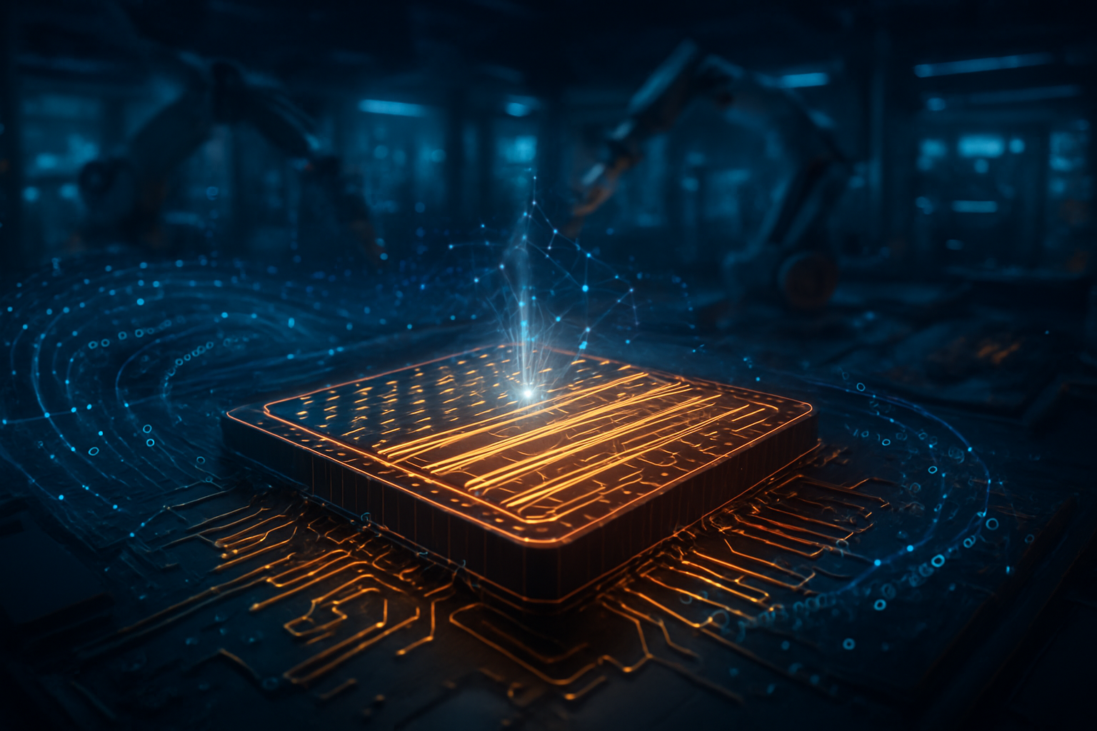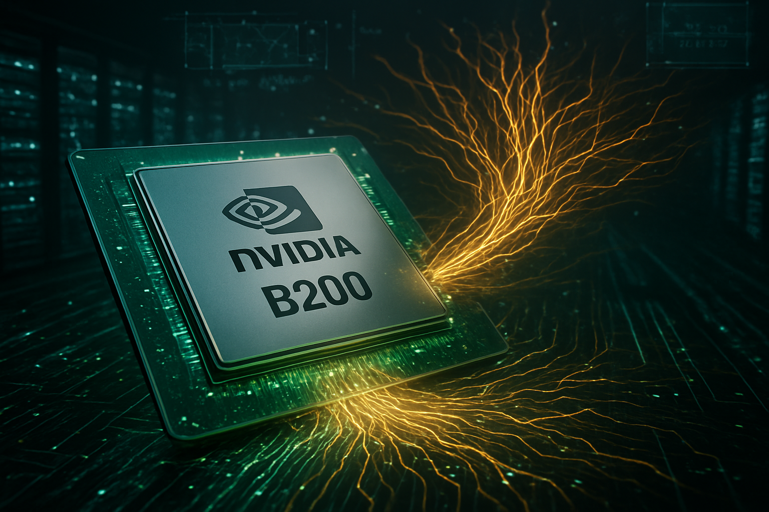
As the world’s leading technology innovators gathered in Las Vegas for CES 2026, one name continued to dominate the conversation: NVIDIA (NASDAQ: NVDA). While the event traditionally highlights consumer gadgets, the spotlight this year remained firmly on the Blackwell B200 architecture, a silicon marvel that has fundamentally reshaped the trajectory of artificial intelligence over the past eighteen months. With a staggering 208 billion transistors and a theoretical 30x performance leap in inference tasks over the previous Hopper generation, Blackwell has transitioned from a high-tech promise into the indispensable backbone of the global AI economy.
The showcase at CES 2026 underscored a pivotal moment in the industry. As hyperscalers scramble to secure every available unit, NVIDIA CEO Jensen Huang confirmed that the Blackwell architecture is effectively sold out through mid-2026. This unprecedented demand highlights a shift in the tech landscape where compute power has become the most valuable commodity on Earth, fueling the transition from basic generative AI to advanced, "agentic" systems capable of complex reasoning and autonomous decision-making.
The Silicon Architecture of the Trillion-Parameter Era
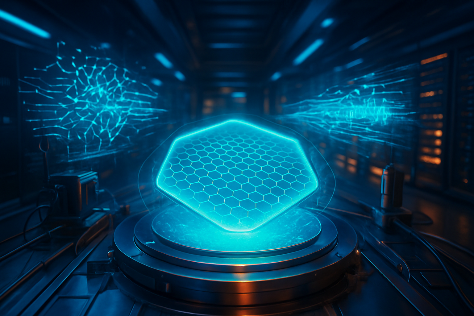
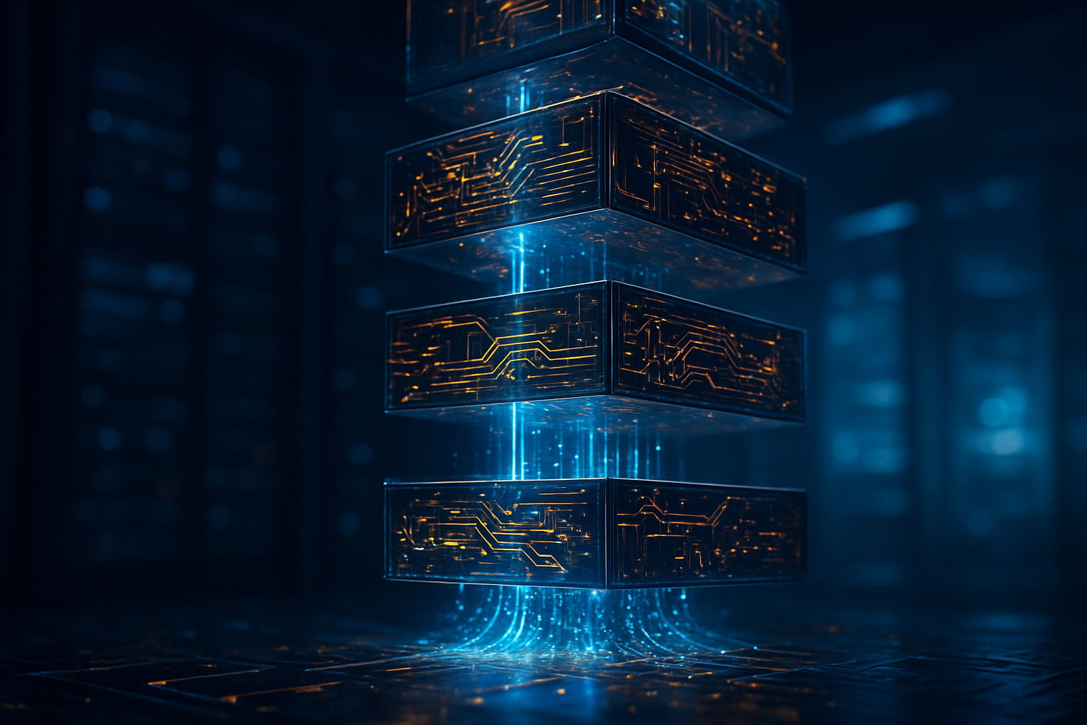
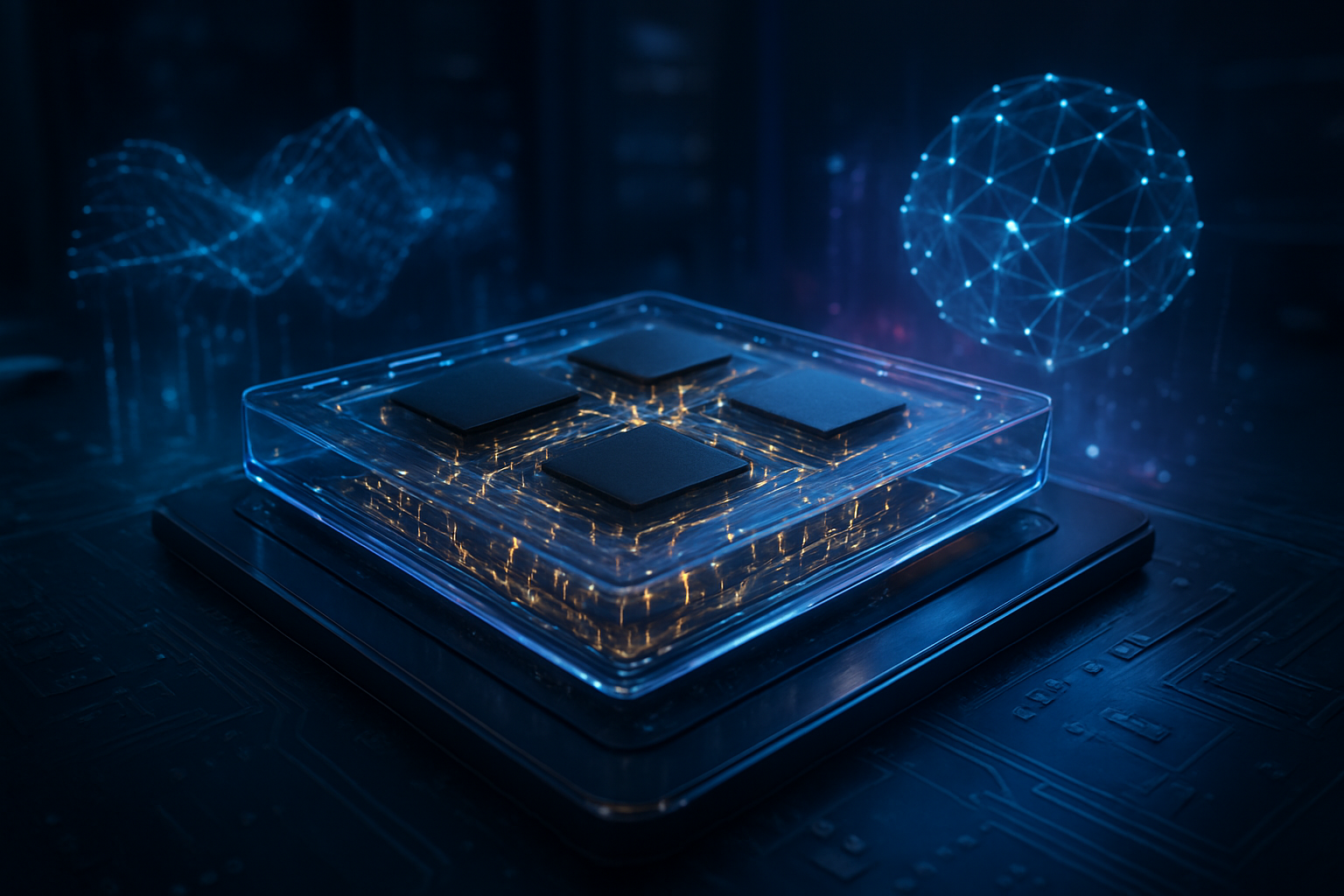
At the heart of the Blackwell B200’s dominance is its radical "chiplet" design, a departure from the monolithic structures of the past. Manufactured on a custom 4NP process by TSMC (NYSE: TSM), the B200 integrates two reticle-limited dies into a single, unified processor via a 10 TB/s high-speed interconnect. This design allows the 208 billion transistors to function with the seamlessness of a single chip, overcoming the physical limitations that have historically slowed down large-scale AI processing. The result is a chip that doesn’t just iterate on its predecessor, the H100, but rather leaps over it, offering up to 20 Petaflops of AI performance in its peak configuration.
Technically, the most significant breakthrough within the Blackwell architecture is the introduction of the second-generation Transformer Engine and support for FP4 (4-bit floating point) precision. By utilizing 4-bit weights, the B200 can double its compute throughput while significantly reducing the memory footprint required for massive models. This is the primary driver behind the "30x inference" claim; for trillion-parameter models like the rumored GPT-5 or Llama 4, Blackwell can process requests at speeds that make real-time, human-like reasoning finally feasible at scale.
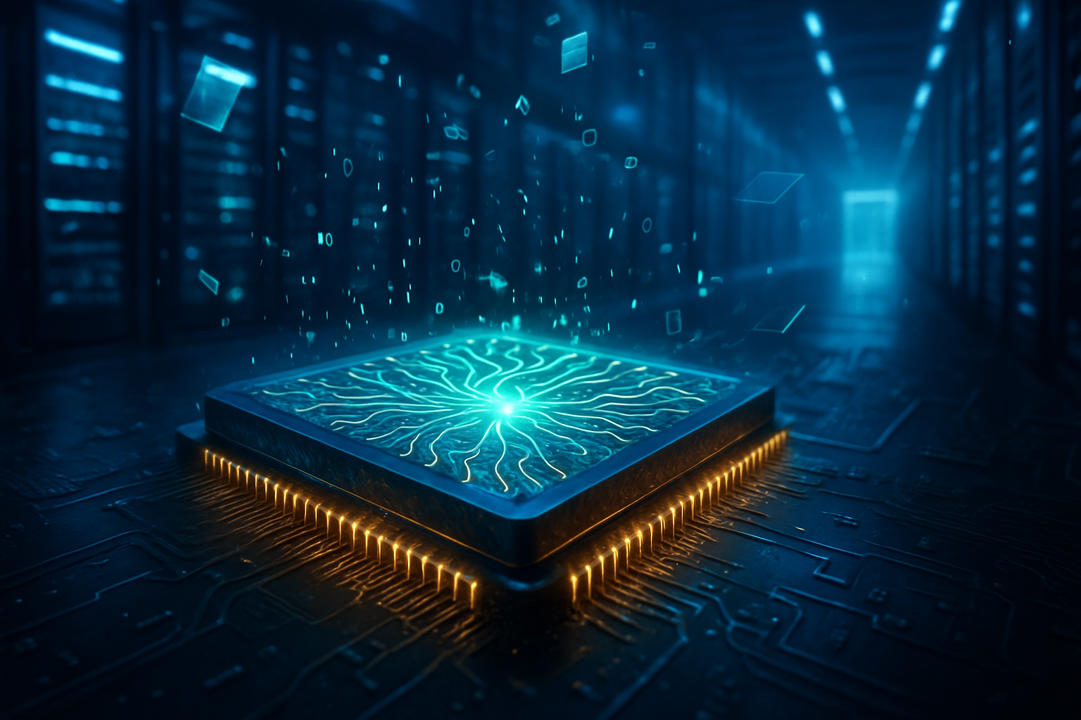
Furthermore, the integration of NVLink 5.0 provides 1.8 TB/s of bidirectional bandwidth per GPU. In the massive "GB200 NVL72" rack configurations showcased at CES, 72 Blackwell GPUs act as a single massive unit with 130 TB/s of aggregate bandwidth. This level of interconnectivity allows AI researchers to treat an entire data center rack as a single GPU, a feat that industry experts suggest has shortened the training time for frontier models from months to mere weeks. Initial reactions from the research community have been overwhelmingly positive, with many noting that Blackwell has effectively "removed the memory wall" that previously hindered the development of truly multi-modal AI systems.
Hyperscalers and the High-Stakes Arms Race
The market dynamics surrounding Blackwell have created a clear divide between the "compute-rich" and the "compute-poor." Major hyperscalers, including Microsoft (NASDAQ: MSFT), Meta (NASDAQ: META), Alphabet (NASDAQ: GOOGL), and Amazon (NASDAQ: AMZN), have moved aggressively to monopolize the supply chain. Microsoft remains a lead customer, integrating the GB200 systems into its Azure infrastructure to power the next generation of OpenAI’s reasoning models. Meanwhile, Meta has confirmed the deployment of hundreds of thousands of Blackwell units to train Llama 4, citing the 1.8 TB/s NVLink as a non-negotiable requirement for synchronizing the massive clusters needed for their open-source ambitions.
For these tech giants, the B200 represents more than just a speed upgrade; it is a strategic moat. By securing vast quantities of Blackwell silicon, these companies can offer AI services at a lower cost-per-query than competitors still reliant on older Hopper or Ampere hardware. This competitive advantage is particularly visible in the startup ecosystem, where new AI labs are finding it increasingly difficult to compete without access to Blackwell-based cloud instances. The sheer efficiency of the B200—which is 25x more energy-efficient than the H100 in certain inference tasks—allows these giants to scale their AI operations without being immediately throttled by the power constraints of existing electrical grids.
A Milestone in the Broader AI Landscape
When viewed through the lens of AI history, the Blackwell generation marks the moment where "Scaling Laws"—the principle that more data and more compute lead to better models—found their ultimate hardware partner. We are moving past the era of simple chatbots and into an era of "physical AI" and autonomous agents. The 30x inference leap means that complex AI "reasoning" steps, which might have taken 30 seconds on a Hopper chip, now happen in one second on Blackwell. This creates a qualitative shift in how users interact with AI, enabling it to function as a real-time assistant rather than a delayed search tool.
There are, however, significant concerns regarding the concentration of power. As NVIDIA’s Blackwell architecture becomes the "operating system" of the AI world, questions about supply chain resilience and energy consumption have moved to the forefront of geopolitical discussions. While the B200 is more efficient on a per-task basis, the sheer scale of the clusters being built is driving global demand for electricity to record highs. Critics point out that the race for Blackwell-level compute is also a race for rare earth minerals and specialized manufacturing capacity, potentially creating new bottlenecks in the global economy.
Comparisons to previous milestones, such as the introduction of the first CUDA-capable GPUs or the launch of the original Transformer model, are common among industry analysts. However, Blackwell is unique because it represents the first time hardware has been specifically co-designed with the mathematical requirements of Large Language Models in mind. By optimizing specifically for the Transformer architecture, NVIDIA has created a self-reinforcing loop where the hardware dictates the direction of AI research, and AI research in turn justifies the massive investment in next-generation silicon.
The Road Ahead: From Blackwell to Vera Rubin
Looking toward the near future, the CES 2026 showcase provided a tantalizing glimpse of what follows Blackwell. NVIDIA has already begun detailing the "Blackwell Ultra" (B300) variant, which features 288GB of HBM3e memory—a 50% increase that will further push the boundaries of long-context AI processing. But the true headline of the event was the formal introduction of the "Vera Rubin" architecture (R100). Scheduled for a late 2026 rollout, Rubin is projected to feature 336 billion transistors and a move to HBM4 memory, offering a staggering 22 TB/s of bandwidth.
In the long term, the applications for Blackwell and its successors extend far beyond text and image generation. Jensen Huang showcased "Alpamayo," a family of "chain-of-thought" reasoning models specifically designed for autonomous vehicles, which will debut in the 2026 Mercedes-Benz fleet. These models require the high-throughput, low-latency processing that only Blackwell-class hardware can provide. Experts predict that the next two years will see a massive shift toward "Edge Blackwell" chips, bringing this level of intelligence directly into robotics, surgical tools, and industrial automation.
The primary challenge ahead remains one of sustainability and distribution. As models continue to grow, the industry will eventually hit a "power wall" that even the most efficient chips cannot overcome. Engineers are already looking toward optical interconnects and even more exotic 3D-stacking techniques to keep the performance gains coming. For now, the focus is on maximizing the potential of the current Blackwell fleet as it enters its most productive phase.
Final Reflections on the Blackwell Revolution
The NVIDIA Blackwell B200 architecture has proved to be the defining technological achievement of the mid-2020s. By delivering a 30x inference performance leap and packing 208 billion transistors into a unified design, NVIDIA has provided the necessary "oxygen" for the AI fire to continue burning. The demand from hyperscalers like Microsoft and Meta is a testament to the chip's transformative power, turning compute capacity into the new currency of global business.
As we look back at the CES 2026 announcements, it is clear that Blackwell was not an endpoint but a bridge to an even more ambitious future. Its legacy will be measured not just in transistor counts or flops, but in the millions of autonomous agents and the scientific breakthroughs it has enabled. In the coming months, the industry will be watching closely as the first Blackwell Ultra units begin to ship and as the race to build the first "million-GPU cluster" reaches its inevitable conclusion. For now, NVIDIA remains the undisputed architect of the intelligence age.
This content is intended for informational purposes only and represents analysis of current AI developments.
TokenRing AI delivers enterprise-grade solutions for multi-agent AI workflow orchestration, AI-powered development tools, and seamless remote collaboration platforms.
For more information, visit https://www.tokenring.ai/.