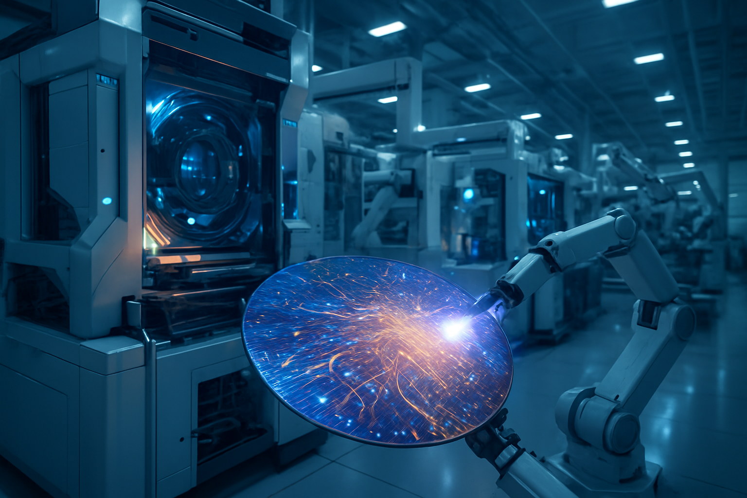
As of January 16, 2026, the artificial intelligence industry has reached a pivotal inflection point where the sheer computational power of GPUs is no longer the primary bottleneck. Instead, the focus has shifted to the "memory wall"—the limit on how fast data can move between memory and processing cores. The resolution to this crisis has arrived in the form of High Bandwidth Memory 4 (HBM4), representing a fundamental transformation of memory from a generic "commodity" component into a highly customized, application-specific silicon platform.
This evolution is being driven by the relentless demands of trillion-parameter models and agentic AI systems that require unprecedented data throughput. Memory giants like SK Hynix (KRX: 000660) and Samsung Electronics (KRX: 005930) are no longer just selling storage; they are co-designing specialized memory stacks that integrate directly with the next generation of AI architectures, most notably NVIDIA (NASDAQ: NVDA)’s newly unveiled Rubin platform. This shift marks the end of the "one-size-fits-all" era for DRAM and the beginning of a bespoke memory age.
The Technical Leap: Doubling the Pipe and Embedding Logic
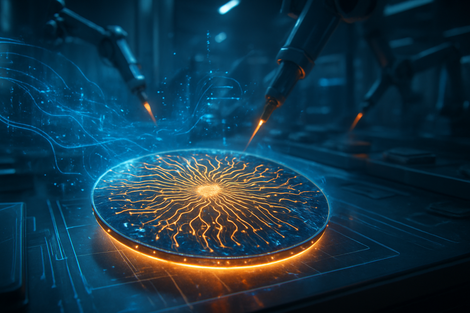
HBM4 is not merely an incremental upgrade over HBM3E; it is an architectural overhaul. The most significant technical specification is the doubling of the physical interface width from 1,024-bit to 2,048-bit. By "widening the pipe" rather than just increasing clock speeds, HBM4 achieves massive gains in bandwidth while maintaining manageable power profiles. Current early-2026 units from Samsung are reporting peak bandwidths of up to 3.25 TB/s per stack, while Micron Technology (NASDAQ: MU) is shipping modules reaching 2.8 TB/s focused on extreme energy efficiency.
Perhaps the most disruptive change is the transition of the "base die" at the bottom of the HBM stack. In previous generations, this die was manufactured using standard DRAM processes. With HBM4, the base die is now being produced on advanced foundry logic nodes, such as the 12nm and 5nm processes from TSMC (NYSE: TSM). This allows for the integration of custom logic directly into the memory stack. Designers can now embed custom memory controllers, hardware-level encryption, and even Processing-in-Memory (PIM) capabilities that allow the memory to perform basic data manipulation before the data even reaches the GPU.
Initially, the industry targeted a 6.4 Gbps pin speed, but as the requirements for NVIDIA’s Rubin GPUs became clearer in late 2025, the specifications were revised upward. We are now seeing pin speeds between 11 and 13 Gbps. Furthermore, the physical constraints have become a marvel of engineering; to fit 12 or 16 layers of DRAM into a JEDEC-standard package height of 775µm, wafers must be thinned to a staggering 30µm—roughly one-third the thickness of a human hair.
A New Competitive Landscape: Alliances vs. Turnkey Solutions
The transition to customized HBM4 has reordered the competitive dynamics of the semiconductor industry. SK Hynix has solidified its market leadership through a "One-Team" alliance with TSMC. By leveraging TSMC’s logic process for the base die, SK Hynix ensures that its memory stacks are perfectly optimized for the Blackwell and Rubin GPUs also manufactured by TSMC. This partnership has allowed SK Hynix to deploy its proprietary Advanced MR-MUF (Mass Reflow Molded Underfill) technology, which offers superior thermal dissipation—a critical factor as 16-layer stacks become the norm for high-end AI servers.
In contrast, Samsung Electronics is doubling down on its "turnkey" strategy. As the only company with its own DRAM production, logic foundry, and advanced packaging facilities, Samsung aims to provide a total solution under one roof. Samsung has become a pioneer in copper-to-copper hybrid bonding for HBM4. This technique eliminates the need for traditional micro-bumps between layers, allowing for even denser stacks with better thermal performance. By using its 4nm logic node for the base die, Samsung is positioning itself as the primary alternative for companies that want to bypass the TSMC-dominated supply chain.
For NVIDIA, this customization is essential. The upcoming Rubin architecture, expected to dominate the second half of 2026, utilizes eight HBM4 stacks per GPU, providing a staggering 288GB of memory and over 22 TB/s of aggregate bandwidth. This "extreme co-design" allows NVIDIA to treat the GPU and its memory as a single coherent pool, which is vital for the low-latency reasoning required by modern "agentic" AI workflows that must process massive amounts of context in real-time.
Solving the Memory Wall for Trillion-Parameter Models
The broader significance of the HBM4 transition cannot be overstated. As AI models move from hundreds of billions to multiple trillions of parameters, the energy cost of moving data between the processor and memory has become the single largest expense in the data center. By moving logic into the HBM base die, manufacturers are effectively reducing the distance data must travel, significantly lowering the total cost of ownership (TCO) for AI labs like OpenAI and Anthropic.
This development also addresses the "KV-cache" bottleneck in Large Language Models (LLMs). As models gain longer context windows—some now reaching millions of tokens—the amount of memory required just to store the intermediate states of a conversation has exploded. Customized HBM4 stacks allow for specialized memory management that can prioritize this data, enabling more efficient "thinking" processes in AI agents without the massive performance hits seen in the HBM3 era.
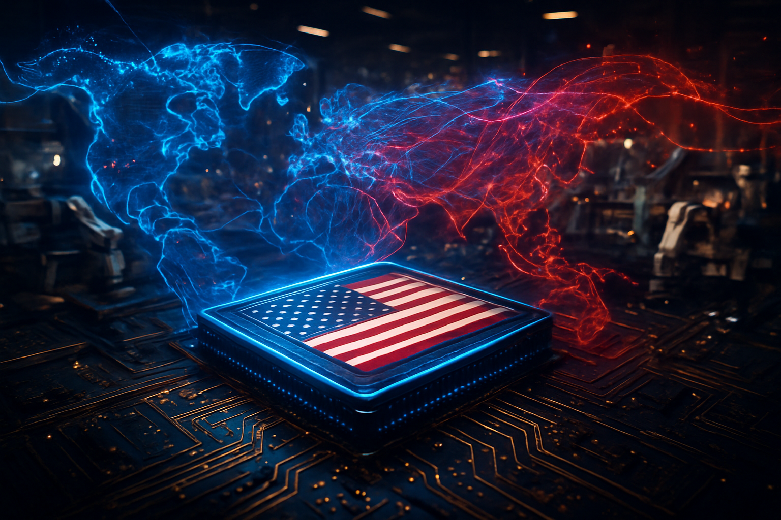
However, the shift to custom memory also raises concerns regarding supply chain flexibility. In the era of commodity memory, a cloud provider could theoretically swap one vendor's RAM for another's. In the era of custom HBM4, the memory is so deeply integrated into the GPU's architecture that switching vendors becomes an arduous engineering task. This deep integration grants NVIDIA and its preferred partners even greater control over the AI hardware ecosystem, potentially raising barriers to entry for new chip startups.
The Horizon: 16-Hi Stacks and Beyond
Looking toward the latter half of 2026 and into 2027, the roadmap for HBM4 is already expanding. While 12-layer (12-Hi) stacks are the current volume leader, SK Hynix recently unveiled 16-Hi prototypes at CES 2026, promising 48GB of capacity per stack. These high-density modules will be the backbone of the "Rubin Ultra" GPUs, which are expected to push total on-chip memory toward the half-terabyte mark.
Experts predict that the next logical step will be the full integration of optical interconnects directly into the HBM stack. This would allow for even faster communication between GPU clusters, effectively turning a whole rack of servers into a single giant GPU. Challenges remain, particularly in the yield rates of hybrid bonding and the thermal management of 16-layer towers of silicon, but the momentum is undeniable.
A New Chapter in Silicon Evolution
The evolution of HBM4 represents a fundamental shift in the hierarchy of computing. Memory is no longer a passive servant to the processor; it has become an active participant in the computational process. The move from commodity DRAM to customized HBM4 platforms is the industry's most potent weapon against the plateauing of Moore’s Law, providing the data throughput necessary to keep the AI revolution on its exponential growth curve.
Key takeaways for the coming months include the ramp-up of Samsung’s hybrid bonding production and the first performance benchmarks of the Rubin architecture in the wild. As we move deeper into 2026, the success of these custom memory stacks will likely determine which hardware platforms can truly support the next generation of autonomous, trillion-parameter AI agents. The memory wall is falling, and in its place, a new, more integrated silicon landscape is emerging.
This content is intended for informational purposes only and represents analysis of current AI developments.
TokenRing AI delivers enterprise-grade solutions for multi-agent AI workflow orchestration, AI-powered development tools, and seamless remote collaboration platforms.
For more information, visit https://www.tokenring.ai/.