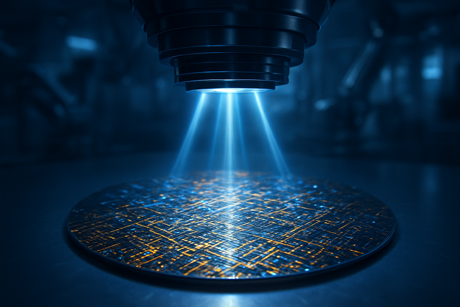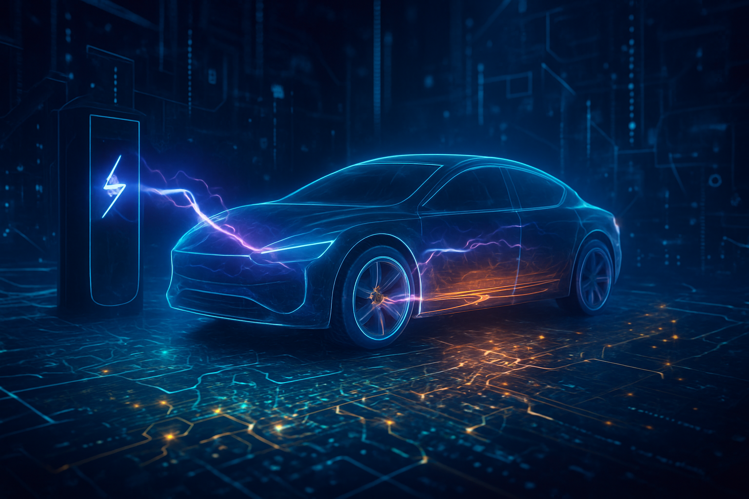
As the global race for semiconductor dominance intensifies, Apple Inc. (NASDAQ: AAPL) has executed a decisive strategic maneuver to consolidate its lead in the mobile and personal computing markets. Recent supply chain reports confirm that Apple has successfully reserved over 50% of the initial 2nm (N2) manufacturing capacity from Taiwan Semiconductor Manufacturing Company (NYSE: TSM / TPE: 2330) for the 2026 calendar year. This multi-billion dollar commitment ensures that Apple will be the first—and for a time, the only—major player with the volume required to bring 2nm-based consumer electronics to the mass market.
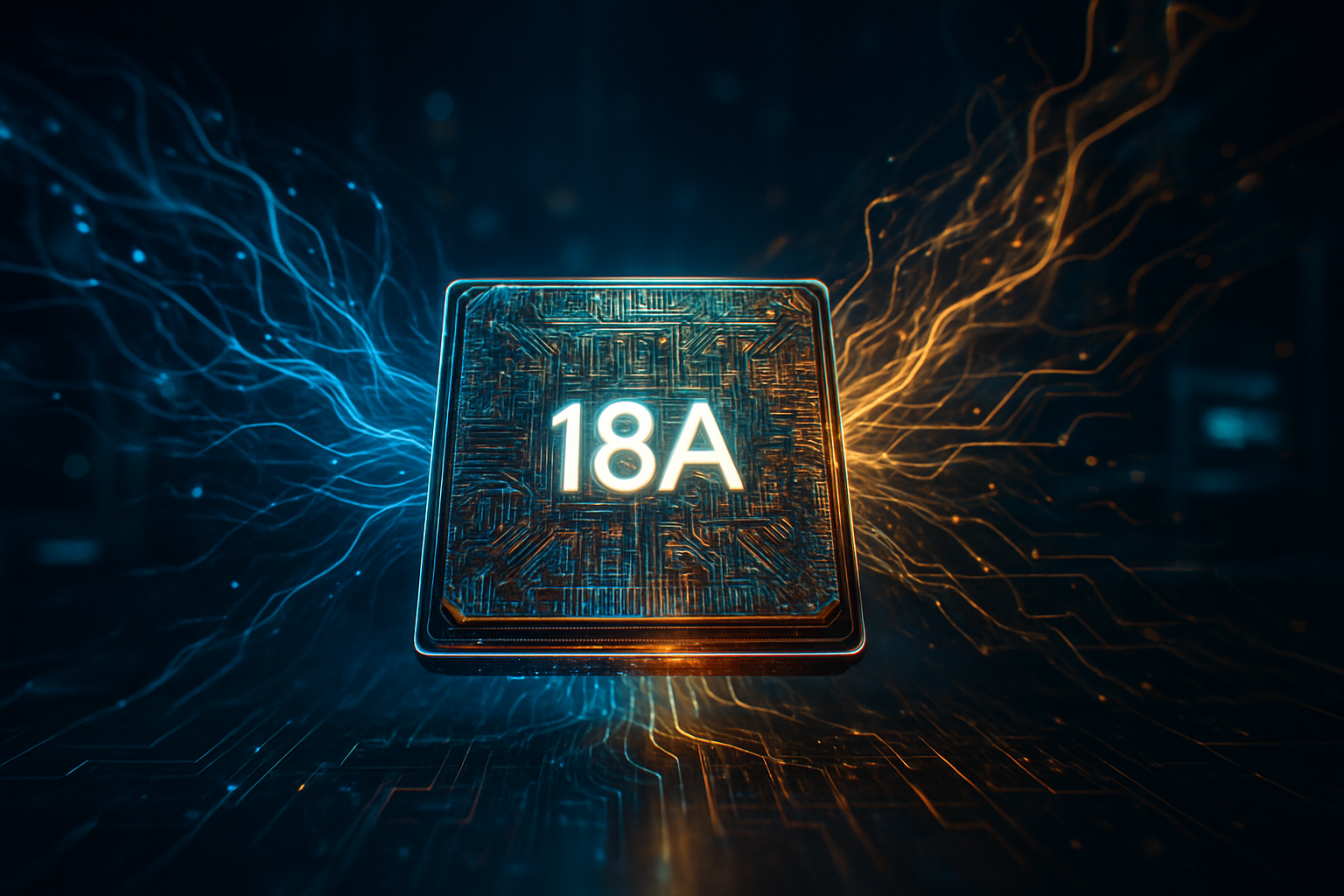
The move marks a critical juncture in the evolution of "on-device AI." By monopolizing the world's most advanced silicon production lines, Apple is positioning its upcoming iPhone 18 and M6-powered MacBooks as the premier platforms for generative AI. This "first-mover" advantage is designed to create a performance and efficiency gap so wide that competitors may struggle to catch up for several hardware cycles, effectively turning the semiconductor supply chain into a defensive moat.
The Dawn of GAAFET: Inside the A20 Pro and M6 Architecture
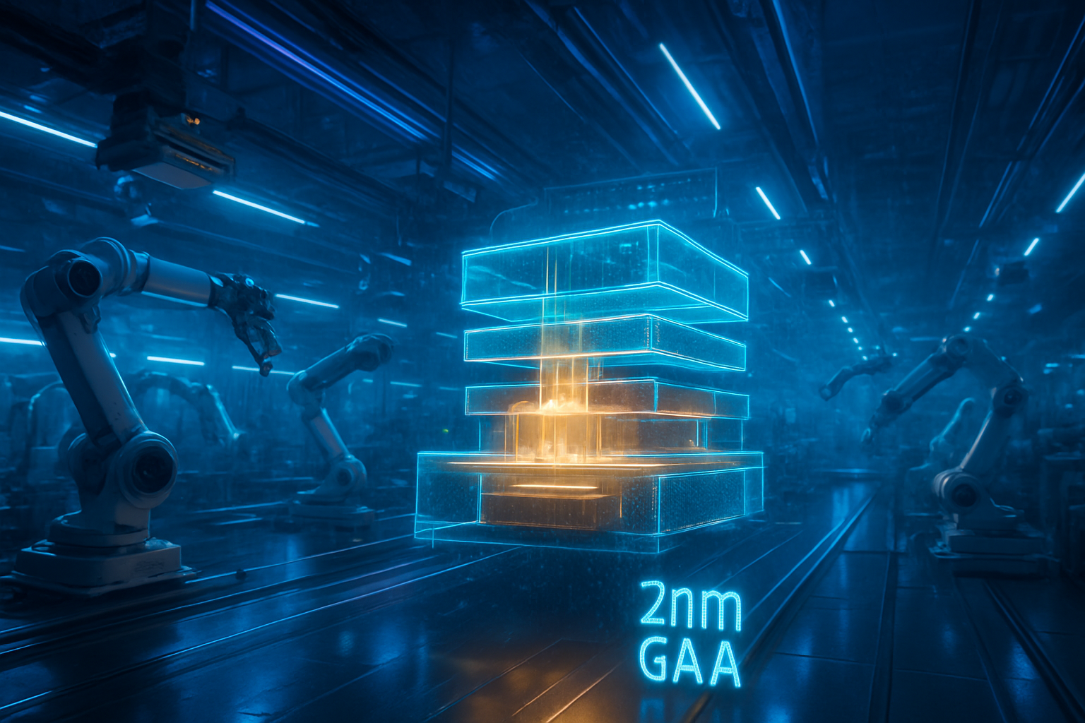
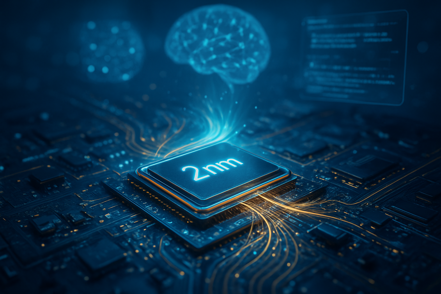
At the heart of this transition is a fundamental shift in transistor technology. After years of utilizing FinFET (Fin Field-Effect Transistor) architecture, the 2nm N2 node introduces Gate-all-around (GAAFET) nanosheet technology. Unlike the previous design where the gate contacted the channel on three sides, GAAFET wraps the gate entirely around the channel. This provides significantly better electrostatic control, drastically reducing current leakage—a primary hurdle for mobile chip performance. Technical specifications for the N2 node suggest a 10–15% speed boost at the same power level or a staggering 25–30% reduction in power consumption compared to the current 3nm (N3P) processes.
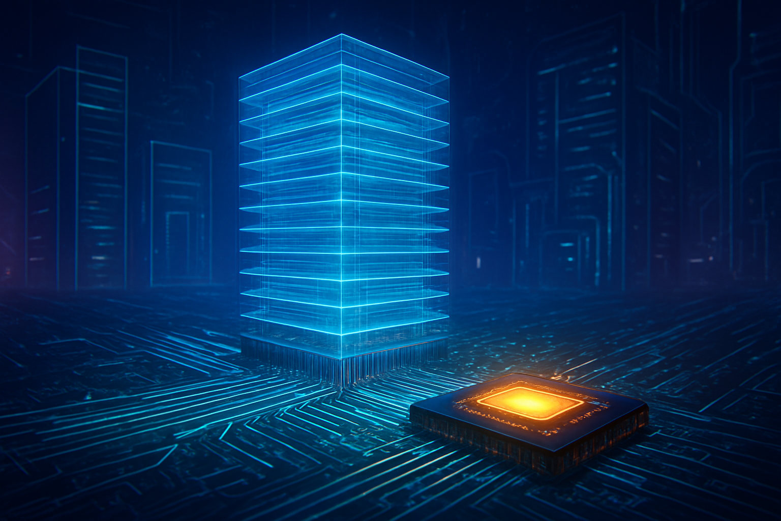
The upcoming A20 Pro chip, slated for the iPhone 18 Pro series in late 2026, is expected to leverage a new Wafer-Level Multi-Chip Module (WMCM) packaging technique. This "RAM-on-Wafer" approach integrates the CPU, GPU, and high-bandwidth memory directly onto a single silicon structure. By reducing the physical distance data must travel between the processor and memory, Apple aims to achieve the ultra-low latency required for real-time generative AI tasks, such as live video translation and complex local LLM (Large Language Model) processing.
Industry experts have reacted with a mix of awe and concern. While the research community praises the engineering feat of mass-producing nanosheet transistors, many note that the barrier to entry for advanced silicon has never been higher. The integration of Super High-Performance Metal-Insulator-Metal (SHPMIM) capacitors within the 2nm node will further stabilize power delivery, allowing the M6 processor family—destined for a redesigned MacBook Pro lineup—to maintain peak performance during heavy AI workloads without the thermal throttling that plagues current-generation competitors.
Strategic Starvation: Depriving the Competition
Apple’s move to seize more than half of TSMC’s initial 2nm output is more than a production necessity; it is a tactical strike against the broader ecosystem. Major chip designers like Qualcomm (NASDAQ: QCOM) and MediaTek (TWSE: 2454) now find themselves in a precarious position. With Apple occupying the majority of the N2 lines, these competitors are reportedly being forced to skip the standard 2nm node and wait for the "N2P" (enhanced 2nm) variant, which is not expected to reach high-volume production until late 2026 or early 2027.
This "strategic starvation" of the supply chain means that for the better part of 2026, flagship Android devices may be relegated to refined versions of 3nm technology while Apple scales the 2nm wall. For Qualcomm, this poses a significant threat to its Snapdragon 8 series market share, particularly as premium smartphone buyers increasingly prioritize battery life and "AI-readiness." MediaTek, which has been making inroads into the high-end market with its Dimensity chips, may see its momentum blunted if it cannot offer a 2nm alternative to global OEMs (Original Equipment Manufacturers).
The market positioning here is clear: Apple is using its massive cash reserves to buy time. By the time Qualcomm and MediaTek can access 2nm at scale, Apple will likely be refining its second-generation 2nm designs or looking toward 1.4nm (A14) prototyping. This cycle of capacity locking prevents a level playing field, ensuring that the most efficient "AI PCs" and smartphones bear the Apple logo during the most critical growth phase of the AI industry.
The Global Semiconductor Chessboard and the AI Landscape
This development fits into a broader trend of "vertical integration" where tech giants no longer just design software, but also dictate the physical limits of their hardware. In the current AI landscape, the bottleneck is no longer just algorithmic; it is thermal and electrical. As generative AI models move from the cloud to the "edge" (on-device), the device with the most efficient transistors wins. Apple’s 2nm reservation is a bet that the future of AI will be won by those who can run the largest models with the smallest battery drain.
However, this concentration of manufacturing power raises concerns regarding supply chain resiliency. With over 50% of the world's most advanced chips destined for a single company, any disruption at TSMC's Hsinchu or Chiayi facilities could have a cascading effect on the global economy. Furthermore, the rising cost of 2nm wafers—rumored to exceed $30,000 per unit—suggests that the "silicon divide" between premium and budget devices will only widen.
The 2nm transition is being compared to the 2012 shift to 28nm, a milestone that redefined mobile computing. But unlike 2012, the stakes today involve national security and global AI leadership. Apple’s aggressive stance highlights the reality that in 2026, silicon is the ultimate currency of power. Those who do not own the capacity are essentially tenants in a landscape owned by the few who can afford the entry price.
Looking Ahead: From 2nm to the 1.4nm Horizon
As we look toward the latter half of 2026, the first 2nm devices will undergo their true test in the hands of consumers. Beyond the iPhone 18 and M6 MacBooks, rumors suggest a second-generation Apple Vision Pro featuring an "R2" chip built on the 2nm process. This would be a game-changer for spatial computing, potentially doubling the device's battery life or enabling the high-fidelity AR rendering that the first generation struggled to maintain.
The long-term roadmap already points toward 1.4nm (A14) production by 2028. TSMC has already begun exploratory work on these "Angstrom-era" nodes, which will likely require even more exotic materials and High-NA EUV (Extreme Ultraviolet) lithography. The challenge for Apple and TSMC will be maintaining yields; as transistors shrink toward the atomic scale, quantum tunneling and heat dissipation become exponentially harder to manage.
Experts predict that the success of the 2nm node will trigger a new wave of "custom silicon" from other giants like Google and Amazon, who may seek to build their own dedicated factories or form tighter alliances with Intel Foundry or Samsung. The next 24 months will determine if Apple’s gamble on 2nm pays off or if the astronomical costs of these chips lead to a plateau in consumer demand.
A New Era of Hardware-Software Synergy
Apple’s reservation of the majority of TSMC’s 2nm capacity is a watershed moment for the technology industry. It represents the final transition from the "mobile-first" era to the "AI-first" era, where hardware specifications are dictated entirely by the requirements of neural networks. By securing the A20 Pro and M6 production lines, Apple has effectively cornered the market on efficiency for the foreseeable future.
The significance of this development in AI history cannot be overstated. It marks the point where the physical limits of silicon became the primary driver of AI capability. As the first 2nm wafers begin to roll off the lines in Taiwan, the tech world will be watching to see if this "first-mover" strategy delivers the revolutionary user experiences Apple has promised.
In the coming months, keep a close eye on TSMC’s yield reports and the response from the Android ecosystem. If Qualcomm and MediaTek cannot secure a viable path to N2P, we may see a significant shift in the competitive landscape of the premium smartphone market. For now, Apple remains the undisputed king of the silicon supply chain, with a clear path to 2026 dominance.
This content is intended for informational purposes only and represents analysis of current AI developments.
TokenRing AI delivers enterprise-grade solutions for multi-agent AI workflow orchestration, AI-powered development tools, and seamless remote collaboration platforms.
For more information, visit https://www.tokenring.ai/.