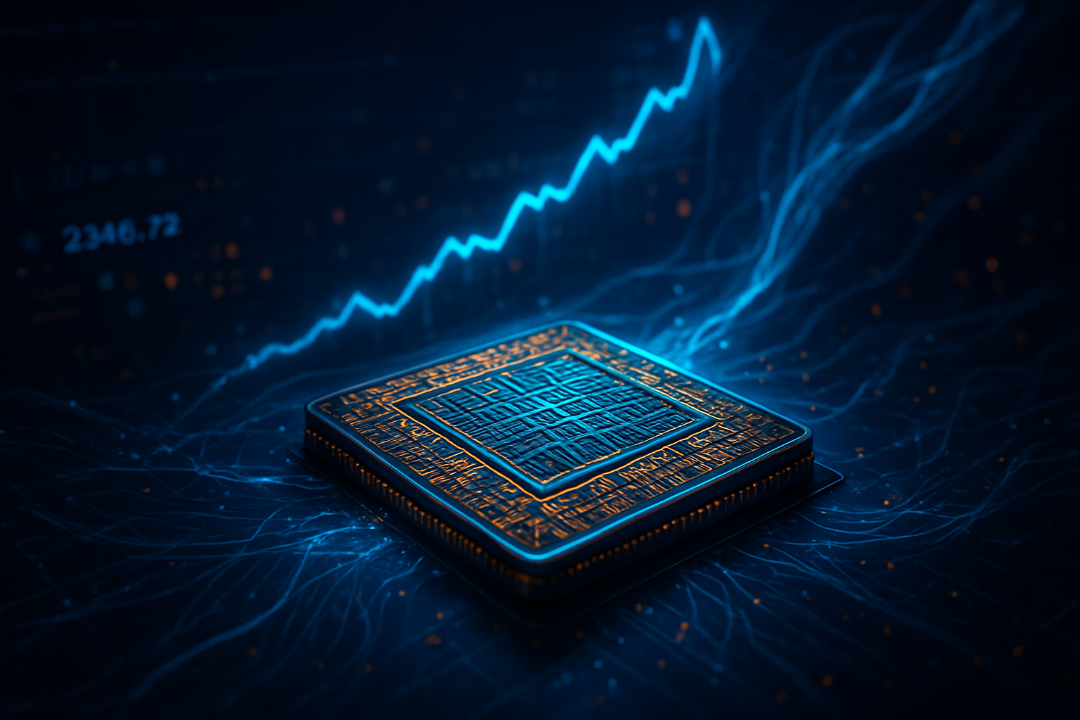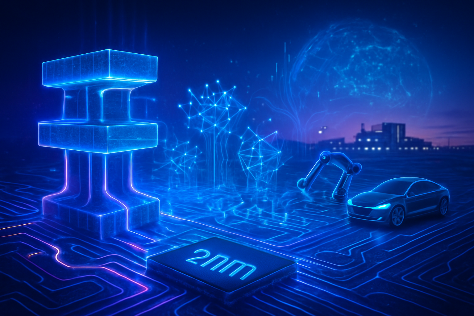
As of January 13, 2026, the semiconductor industry has officially entered the "Angstrom Era," a transition marked by the most significant architectural overhaul in over a decade. For fifty years, chipmakers have followed a "front-side" logic: transistors are built on a silicon wafer, and then layers of intricate copper wiring for both data signals and power are stacked on top. However, as AI accelerators and processors shrink toward the sub-2nm threshold, this traditional "spaghetti" of overlapping wires has become a physical bottleneck, leading to massive voltage drops and heat-related performance throttling.
The solution, now being deployed in high-volume manufacturing by industry leaders, is Backside Power Delivery Network (BSPDN). By flipping the wafer and moving the power delivery grid to the bottom—decoupling it entirely from the signal wiring—foundries are finally breaking through the "Power Wall" that has long threatened to stall the AI revolution. This architectural shift is not merely a refinement; it is a fundamental restructuring of the silicon floorplan that enables the next generation of 1,000W+ AI GPUs and hyper-efficient mobile processors.
The Technical Duel: Intel’s PowerVia vs. TSMC’s Super Power Rail
At the heart of this transition is a fierce technical rivalry between Intel (NASDAQ: INTC) and Taiwan Semiconductor Manufacturing Company (NYSE: TSM). Intel has successfully claimed a "first-mover" advantage with its PowerVia technology, integrated into the Intel 18A (1.8nm) node. PowerVia utilizes "Nano-TSVs" (Through-Silicon Vias) that tunnel through the silicon from the backside to connect to the metal layers just above the transistors. This implementation has allowed Intel to achieve a 30% reduction in platform voltage droop and a 6% boost in clock frequency at identical power levels. By January 2026, Intel’s 18A is in high-volume manufacturing, powering the "Panther Lake" and "Clearwater Forest" chips, effectively proving that BSPDN is viable for mass-market consumer and server silicon.
TSMC, meanwhile, has taken a more complex and potentially more rewarding path with its A16 (1.6nm) node, featuring the Super Power Rail. Unlike Intel’s Nano-TSVs, TSMC’s architecture uses a "Direct Backside Contact" method, where power lines connect directly to the source and drain terminals of the transistors. While this requires extreme manufacturing precision and alignment, it offers superior performance metrics: an 8–10% speed increase and a 15–20% power reduction compared to their previous N2P node. TSMC is currently in the final stages of risk production for A16, with full-scale manufacturing expected in the second half of 2026, targeting the absolute limits of power integrity for high-performance computing (HPC).
Initial reactions from the AI research community have been overwhelmingly positive, with experts noting that BSPDN effectively "reclaims" 20% to 30% of the front-side metal layers. This allows chip designers to use the newly freed space for more complex signal routing, which is critical for the high-bandwidth memory (HBM) and interconnects required for large language model (LLM) training. The industry consensus is that while Intel won the race to market, TSMC’s direct-contact approach may set the gold standard for the most demanding AI accelerators of 2027 and beyond.
Shifting the Competitive Balance: Winners and Losers in the Foundry War
The arrival of BSPDN has drastically altered the strategic positioning of the world’s largest tech companies. Intel’s successful execution of PowerVia on 18A has restored its credibility as a leading-edge foundry, securing high-profile "AI-first" customers like Microsoft (NASDAQ: MSFT) and Amazon (NASDAQ: AMZN). These companies are utilizing Intel’s 18A to develop custom AI accelerators, seeking to reduce their reliance on off-the-shelf hardware by leveraging the density and power efficiency gains that only BSPDN can provide. For Intel, this is a "make-or-break" moment to regain the process leadership it lost to TSMC nearly a decade ago.
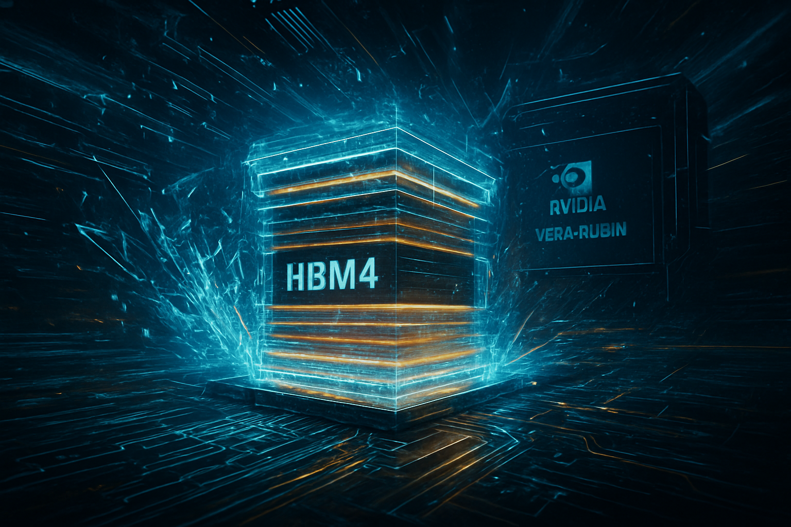
TSMC, however, remains the primary partner for the AI heavyweights. NVIDIA (NASDAQ: NVDA) has reportedly signed on as the anchor customer for TSMC’s A16 node for its 2027 "Feynman" GPU architecture. As AI chips push toward 2,000W power envelopes, NVIDIA’s strategic advantage lies in TSMC’s Super Power Rail, which minimizes the electrical resistance that would otherwise cause catastrophic heat generation. Similarly, AMD (NASDAQ: AMD) is expected to adopt a modular approach, using TSMC’s N2 for general logic while reserving the A16 node for high-performance compute chiplets in its upcoming MI400 series.
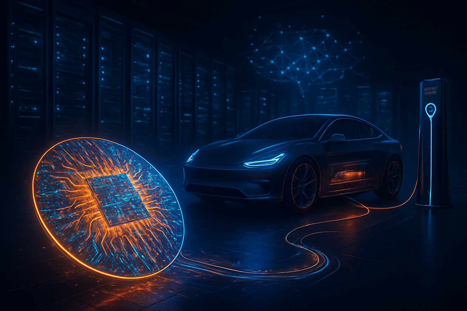
Samsung (KRX: 005930), the third major player, is currently playing catch-up. While Samsung’s SF2 (2nm) node is in mass production and powering the latest Exynos mobile chips, it uses only "preliminary" power rail optimizations. Samsung’s full BSPDN implementation, SF2Z, is not scheduled until 2027. To remain competitive, Samsung has aggressively slashed its 2nm wafer prices to attract cost-conscious AI startups and automotive giants like Tesla (NASDAQ: TSLA), positioning itself as the high-volume, lower-cost alternative to TSMC’s premium A16 pricing.
The Wider Significance: Breaking the Power Wall and Enabling AI Scaling
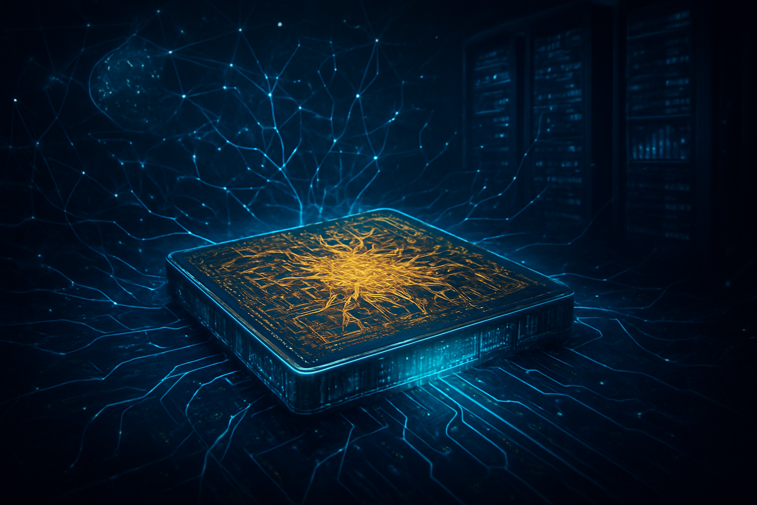
The broader significance of Backside Power Delivery cannot be overstated; it is the "Great Flip" that saves Moore’s Law from thermal death. As transistors have shrunk, the wires connecting them have become so thin that their electrical resistance has skyrocketed. This has led to the "Power Wall," where a chip’s performance is limited not by how many transistors it has, but by how much power can be fed to them without the chip melting. BSPDN solves this by providing a "fat," low-resistance highway for electricity on the back of the chip, reducing the IR drop (voltage drop) by up to 7x.
This development fits into a broader trend of "3D Silicon" and advanced packaging. By thinning the silicon wafer to just a few micrometers to allow for backside access, the heat-generating transistors are placed physically closer to the cooling solutions—such as liquid cold plates—on the back of the chip. This improved thermal proximity is essential for the 2026-2027 generation of data centers, where power density is the primary constraint on AI training capacity.
Compared to previous milestones like the introduction of FinFET transistors in 2011, the move to BSPDN is considered more disruptive because it requires a complete overhaul of the Electronic Design Automation (EDA) tools used by engineers. Design teams at companies like Synopsys (NASDAQ: SNPS) and Cadence (NASDAQ: CDNS) have had to rewrite their software to handle "backside-aware" placement and routing, a change that will define chip design for the next twenty years.
Future Horizons: High-NA EUV and the Path to 1nm
Looking ahead, the synergy between BSPDN and High-Numerical Aperture (High-NA) EUV lithography will define the path to the 1nm (10 Angstrom) frontier. Intel is currently the leader in this integration, already sampling its 14A node which combines High-NA EUV with an evolved version of PowerVia. While High-NA EUV allows for the printing of smaller features, it also makes those features more electrically fragile; BSPDN acts as the necessary electrical support system that makes these microscopic features functional.
In the near term, expect to see "Hybrid Backside" approaches, where not just power, but also certain clock signals and global wires are moved to the back of the wafer. This would further reduce noise and interference, potentially allowing for the first 6GHz+ mobile processors. However, challenges remain, particularly regarding the structural integrity of ultra-thin wafers and the complexity of testing chips from both sides. Experts predict that by 2028, backside delivery will be standard for all high-end silicon, from the chips in your smartphone to the massive clusters powering the next generation of General Artificial Intelligence.
Conclusion: A New Foundation for the Intelligence Age
The transition to Backside Power Delivery marks the end of the "Planar Power" era and the beginning of a truly three-dimensional approach to semiconductor architecture. By decoupling power from signal, Intel and TSMC have provided the industry with a new lease on life, enabling the sub-2nm scaling that is vital for the continued growth of AI. Intel’s early success with PowerVia has tightened the race for process leadership, while TSMC’s ambitious Super Power Rail ensures that the ceiling for AI performance continues to rise.
As we move through 2026, the key metrics to watch will be the manufacturing yields of TSMC’s A16 node and the adoption rate of Intel’s 18A by external foundry customers. The "Great Flip" is more than a technical curiosity; it is the hidden infrastructure that will determine which companies lead the next decade of AI innovation. The foundation of the intelligence age is no longer just on top of the silicon—it is now on the back.
This content is intended for informational purposes only and represents analysis of current AI developments.
TokenRing AI delivers enterprise-grade solutions for multi-agent AI workflow orchestration, AI-powered development tools, and seamless remote collaboration platforms.
For more information, visit https://www.tokenring.ai/.