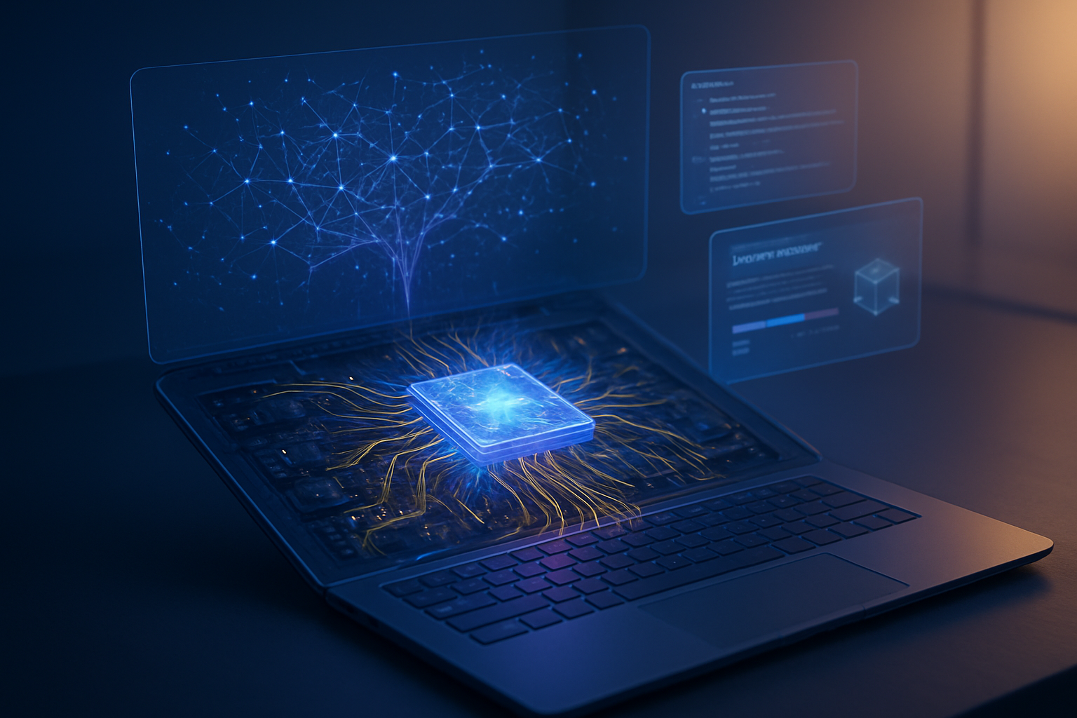
The dream of a truly personal computer—one that understands, anticipates, and assists without tethering itself to a distant data center—has finally arrived. As of January 2026, the "AI PC" is no longer a futuristic marketing buzzword or a premium niche; it has become the standard for modern computing. This week at CES 2026, the industry witnessed a definitive shift as the latest silicon from the world’s leading chipmakers officially moved the heavy lifting of artificial intelligence from the cloud directly onto the local silicon of our laptops and desktops.
This transformation marks the most significant architectural shift in personal computing since the introduction of the graphical user interface. By integrating dedicated Neural Processing Units (NPUs) directly into the heart of the processor, companies like Intel and AMD have enabled a new class of "always-on" AI experiences. From real-time, multi-language translation during live calls to the local generation of high-resolution video, the AI PC era is fundamentally changing how we interact with technology, prioritizing privacy, reducing latency, and slashing the massive energy costs associated with cloud-based AI.
The Silicon Arms Race: Panther Lake vs. Gorgon Point
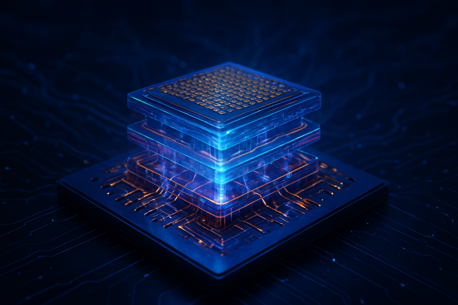
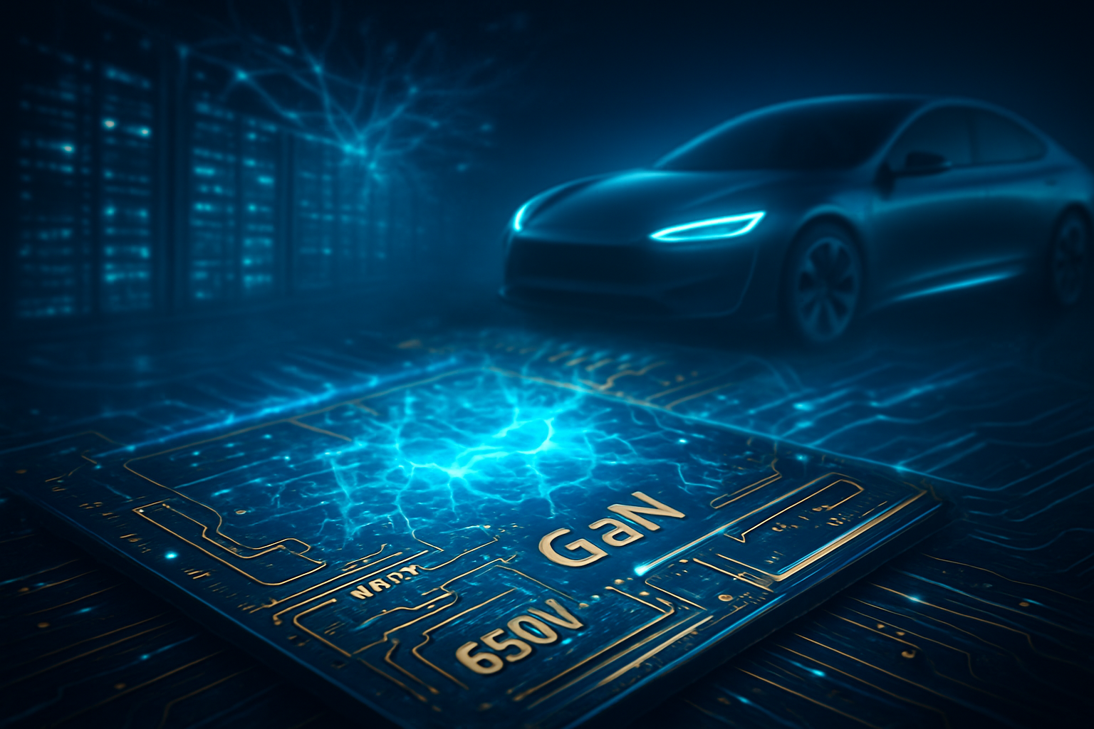
The technical foundation of this era rests on the unprecedented performance of new NPUs. Intel (NASDAQ: INTC) recently unveiled its Core Ultra Series 3, codenamed "Panther Lake," built on the cutting-edge Intel 18A manufacturing process. These chips feature the "NPU 5" architecture, which delivers a consistent 50 Trillions of Operations Per Second (TOPS) dedicated solely to AI tasks. When combined with the new Xe3 "Celestial" GPU and the high-efficiency CPU cores, the total platform performance can reach a staggering 180 TOPS. This allows Panther Lake to handle complex "Physical AI" tasks—such as real-time gesture tracking and environment mapping—without breaking a thermal sweat.
Not to be outdone, AMD (NASDAQ: AMD) has launched its Ryzen AI 400 series, featuring the "Gorgon Point" architecture. AMD’s strategy has focused on "AI ubiquity," bringing high-performance NPUs to even mid-range and budget-friendly laptops. The Gorgon Point chips utilize an upgraded XDNA 2 NPU capable of 60 TOPS, slightly edging out Intel in raw NPU throughput for small language models (SLMs). This hardware allows Windows 11 to run advanced features like "Cocreator" and "Restyle Image" near-instantly, using local weights rather than sending data to a remote server.
This shift differs from previous approaches by moving away from "General Purpose" computing. In the past, AI tasks were offloaded to the GPU, which, while powerful, is a massive power drain. The NPU is a specialized "XPU" designed specifically for the matrix mathematics required by neural networks. Initial reactions from the research community have been overwhelmingly positive, with experts noting that the 2026 generation of chips finally provides the "thermal headroom" necessary for AI to run in the background 24/7 without killing battery life.
A Seismic Shift in the Tech Power Structure
The rise of the AI PC is creating a new hierarchy among tech giants. Microsoft (NASDAQ: MSFT) stands as perhaps the biggest beneficiary, having successfully transitioned its entire Windows ecosystem to the "Copilot+ PC" standard. By mandating a minimum of 40 NPU TOPS for its latest OS features, Microsoft has effectively forced a hardware refresh cycle. This was perfectly timed with the end of support for Windows 10 in late 2025, leading to a massive surge in enterprise upgrades. Businesses are now pivoting toward AI PCs to reduce "inference debt"—the recurring costs of paying for cloud-based AI APIs from providers like OpenAI or Google (NASDAQ: GOOGL).
The competitive implications are equally stark for the mobile-first chipmakers. While Qualcomm (NASDAQ: QCOM) sparked the AI PC trend in 2024 with the Snapdragon X Elite, the 2026 resurgence of x86 dominance from Intel and AMD shows that traditional chipmakers have successfully closed the efficiency gap. By leveraging advanced nodes like Intel 18A, x86 chips now offer the same "all-day" battery life as ARM-based alternatives while maintaining superior compatibility with legacy enterprise software. This has put pressure on Apple (NASDAQ: AAPL), which, despite pioneering integrated NPUs with its M-series, now faces a Windows ecosystem that is more open and increasingly competitive in AI performance-per-watt.
Furthermore, software giants like Adobe (NASDAQ: ADBE) are being forced to re-architect their creative suites. Instead of relying on "Cloud Credits" for generative fill or video upscaling, the 2026 versions of Photoshop and Premiere Pro are optimized to detect the local NPU. This disrupts the current SaaS (Software as a Service) model, shifting the value proposition from cloud-based "magic" to local, hardware-accelerated productivity.
Privacy, Latency, and the Death of the Cloud Tether
The wider significance of the AI PC era lies in the democratization of privacy. In 2024, Microsoft faced significant backlash over "Windows Recall," a feature that took snapshots of user activity. In 2026, the narrative has flipped. Thanks to the power of local NPUs, Recall data is now encrypted and stored in a "Secure Zone" on the chip, never leaving the device. This "Local-First" AI model is a direct response to growing consumer anxiety over data harvesting. When your PC translates a private business call or generates a sensitive document locally, the risk of a data breach is virtually eliminated.
Beyond privacy, the impact on global bandwidth is profound. As AI PCs handle more generative tasks locally, the strain on global data centers is expected to plateau. This fits into the broader "Edge AI" trend, where intelligence is pushed to the periphery of the network. We are seeing a move away from the "Thin Client" philosophy of the last decade and a return to the "Fat Client," where the local machine is the primary engine of creation.
However, this transition is not without concerns. There is a growing "AI Divide" between those who can afford the latest NPU-equipped hardware and those stuck on "legacy" systems. As software developers increasingly optimize for NPUs, older machines may feel significantly slower, not because their CPUs are weak, but because they lack the specialized silicon required for the modern, AI-integrated operating system.
The Road Ahead: Agentic AI and Physical Interaction
Looking toward the near future, the next frontier for the AI PC is "Agentic AI." While today’s systems are reactive—responding to prompts—the late 2026 and 2027 roadmaps suggest a shift toward proactive agents. These will be local models that observe your workflow across different apps and perform complex, multi-step tasks autonomously, such as "organizing all receipts from last month into a spreadsheet and flagging discrepancies."
We are also seeing the emergence of "Physical AI" applications. With the high TOPS counts of 2026 hardware, PCs are becoming capable of processing high-fidelity spatial data. This will enable more immersive augmented reality (AR) integrations and sophisticated eye-tracking and gesture-based interfaces that feel natural rather than gimmicky. The challenge remains in standardization; while Microsoft has set the baseline with Copilot+, a unified API that allows developers to write one AI application that runs seamlessly across Intel, AMD, and Qualcomm silicon is still a work in progress.
A Landmark Moment in Computing History
The dawn of the AI PC era represents the final transition of the computer from a tool we use to a collaborator we work with. The developments seen in early 2026 confirm that the NPU is now as essential to the motherboard as the CPU itself. The key takeaways are clear: local AI is faster, more private, and increasingly necessary for modern software.
As we look ahead, the significance of this milestone will likely be compared to the transition from command-line interfaces to Windows. The AI PC has effectively "humanized" the machine. In the coming months, watch for the first wave of "NPU-native" applications that move beyond simple chatbots and into true, local workflow automation. The "Crossover Year" has passed, and the era of the intelligent, autonomous personal computer is officially here.
This content is intended for informational purposes only and represents analysis of current AI developments.
TokenRing AI delivers enterprise-grade solutions for multi-agent AI workflow orchestration, AI-powered development tools, and seamless remote collaboration platforms.
For more information, visit https://www.tokenring.ai/.