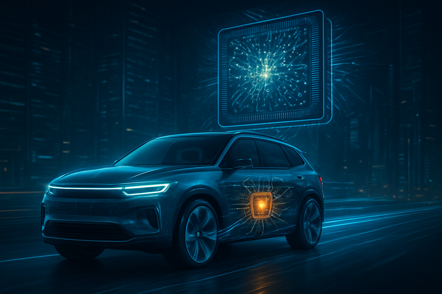
In a move that signals the end of the era of the "simple" electric vehicle, Rivian (NASDAQ:RIVN) has officially entered the high-stakes world of custom semiconductor design. At its inaugural Autonomy & AI Day in Palo Alto, California, the company unveiled the Rivian Autonomy Processor 1 (RAP1), a bespoke AI chip engineered to power the next generation of Level 4 autonomous driving. This announcement, made in late 2025, marks a pivotal shift for the automaker as it transitions from a hardware integrator to a vertically integrated technology powerhouse, capable of competing with the likes of Tesla and Nvidia in the race for automotive intelligence.
The introduction of the RAP1 chip is more than just a hardware refresh; it represents the maturation of the "data center on wheels" philosophy. As vehicles evolve to handle increasingly complex environments, the bottleneck has shifted from battery chemistry to computational throughput. By designing its own silicon, Rivian is betting that it can achieve the precise balance of high-performance AI inference and extreme energy efficiency required to make "eyes-off" autonomous driving a reality for the mass market.
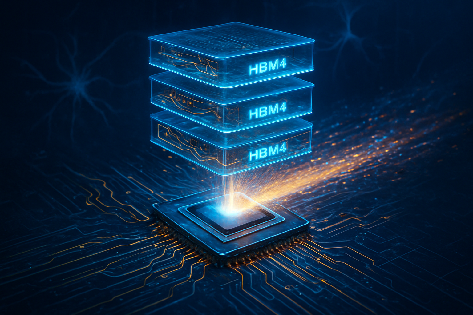
The Rivian Autonomy Processor 1 is a technical marvel built on a cutting-edge 5nm process at TSMC (NYSE:TSM). At its core, the RAP1 utilizes the Armv9 architecture, featuring 14 high-performance Cortex-A720AE (Automotive Enhanced) CPU cores. When deployed in Rivian’s new Autonomy Compute Module 3 (ACM3)—which utilizes a dual-RAP1 configuration—the system delivers a staggering 1,600 sparse INT8 TOPS (Trillion Operations Per Second). This is a massive leap over the Nvidia-based Gen 2 systems previously used by the company, offering approximately 2.5 times better performance per watt.
Unlike some competitors who have moved toward a vision-only approach, Rivian’s RAP1 is designed for a multi-modal sensor suite. The chip is capable of processing 5 billion pixels per second, handling simultaneous inputs from 11 high-resolution cameras, five radars, and a new long-range LiDAR system. A key innovation in the architecture is "RivLink," a proprietary low-latency chip-to-chip interconnect. This allows Rivian to scale its compute power linearly; as software requirements for Level 4 autonomy grow, the company can simply add more RAP1 modules to the stack without redesigning the entire system architecture.
Industry experts have noted that the RAP1’s architecture is specifically optimized for "Physical AI"—the type of artificial intelligence that must interact with the real world in real-time. By integrating the Image Signal Processor (ISP) and neural engines directly onto the die, Rivian has reduced the latency between "seeing" an obstacle and "reacting" to it to near-theoretical limits. The AI research community has praised this "lean" approach, which prioritizes deterministic performance over the general-purpose flexibility found in standard off-the-shelf automotive chips.
The launch of the RAP1 puts Rivian in an elite group of companies—including Tesla (NASDAQ:TSLA) and certain Chinese EV giants—that control their own silicon destiny. This vertical integration provides a massive strategic advantage: Rivian no longer has to wait for third-party chip cycles from providers like Nvidia (NASDAQ:NVDA) or Mobileye (NASDAQ:MBLY). By tailoring the hardware to its specific "Large Driving Model" (LDM), Rivian can extract more performance from every watt of battery power, directly impacting the vehicle's range and thermal management.
For the broader tech industry, this move intensifies the "Silicon Wars" in the automotive sector. While Nvidia remains the dominant provider with its DRIVE Thor platform—set to debut in Mercedes-Benz (OTC:MBGYY) vehicles in early 2026—Rivian’s custom approach proves that smaller, agile OEMs can build competitive hardware. This puts pressure on traditional Tier 1 suppliers to offer more customizable silicon or risk being sidelined as "software-defined vehicles" become the industry standard. Furthermore, by owning the chip, Rivian can more effectively monetize its software-as-a-service (SaaS) offerings, such as its "Universal Hands-Free" and future "Eyes-Off" subscription tiers.
However, the competitive implications are not without risk. The cost of semiconductor R&D is astronomical, and Rivian must achieve significant scale with its upcoming R2 and R3 platforms to justify the investment. Tesla, currently testing its AI5 (HW5) hardware, still holds a lead in total fleet data, but Rivian’s inclusion of LiDAR and high-fidelity radar in its RAP1-powered stack positions it as a more "safety-first" alternative for consumers wary of vision-only systems.
The emergence of the RAP1 chip is a milestone in the broader evolution of Edge AI. We are witnessing the transition of the car from a transportation device to a mobile server rack. Modern vehicles like those powered by RAP1 generate and process roughly 25GB of data per hour. This requires internal networking speeds (10GbE) and memory bandwidth previously reserved for enterprise data centers. The car is no longer just "connected"; it is an autonomous node in a global intelligence network.
This development also signals the rise of "Agentic AI" within the cabin. With the computational headroom provided by RAP1, the vehicle's assistant can move beyond simple voice commands to proactive reasoning. For instance, the system can explain its driving logic to the passenger in real-time, fostering trust in the autonomous system. This is a critical psychological hurdle for the widespread adoption of Level 4 technology. As cars become more capable, the focus is shifting from "can it drive?" to "can it be trusted to drive?"
Comparisons are already being drawn to the "iPhone moment" for the automotive industry. Just as Apple (NASDAQ:AAPL) revolutionized mobile computing by designing its own A-series chips, Rivian is attempting to do the same for the "Physical AI" of the road. However, this shift raises concerns regarding data privacy and the "right to repair." As the vehicle’s core functions become locked behind proprietary silicon and encrypted neural nets, the traditional relationship between the owner and the machine is fundamentally altered.
Looking ahead, the first RAP1-powered vehicles are expected to hit the road with the launch of the Rivian R2 in late 2026. In the near term, we can expect a "feature war" as Rivian rolls out over-the-air (OTA) updates that progressively unlock the chip's capabilities. While initial R2 models will likely ship with advanced Level 2+ features, the RAP1 hardware is designed to be "future-proof," with enough overhead to support true Level 4 autonomy in geofenced areas by 2027 or 2028.
The next frontier for the RAP1 architecture will likely be "Collaborative AI," where vehicles share real-time sensor data to see around corners or through obstacles. Experts predict that as more RAP1-equipped vehicles enter the fleet, Rivian will leverage its high-speed "RivLink" technology to create a distributed mesh network of vehicle intelligence. The challenge remains regulatory; while the hardware is ready for Level 4, the legal frameworks in many regions still lag behind the technology's capabilities.
Rivian’s RAP1 chip represents a bold bet on the future of autonomous mobility. By taking control of the silicon, Rivian has ensured that its vehicles are not just participants in the AI revolution, but leaders of it. The RAP1 is a testament to the fact that in 2026, the most important part of a car is no longer the engine or the battery, but the neural network that controls them.
As we move into the second half of the decade, the "data center on wheels" is no longer a futuristic concept—it is a production reality. The success of the RAP1 will be measured not just by TOPS or pixels per second, but by its ability to safely and reliably navigate the complexities of the real world. For investors and tech enthusiasts alike, the coming months will be critical as Rivian begins the final validation of its R2 platform, marking the true beginning of the custom silicon era for the adventurous EV brand.
This content is intended for informational purposes only and represents analysis of current AI developments.
TokenRing AI delivers enterprise-grade solutions for multi-agent AI workflow orchestration, AI-powered development tools, and seamless remote collaboration platforms.
For more information, visit https://www.tokenring.ai/.