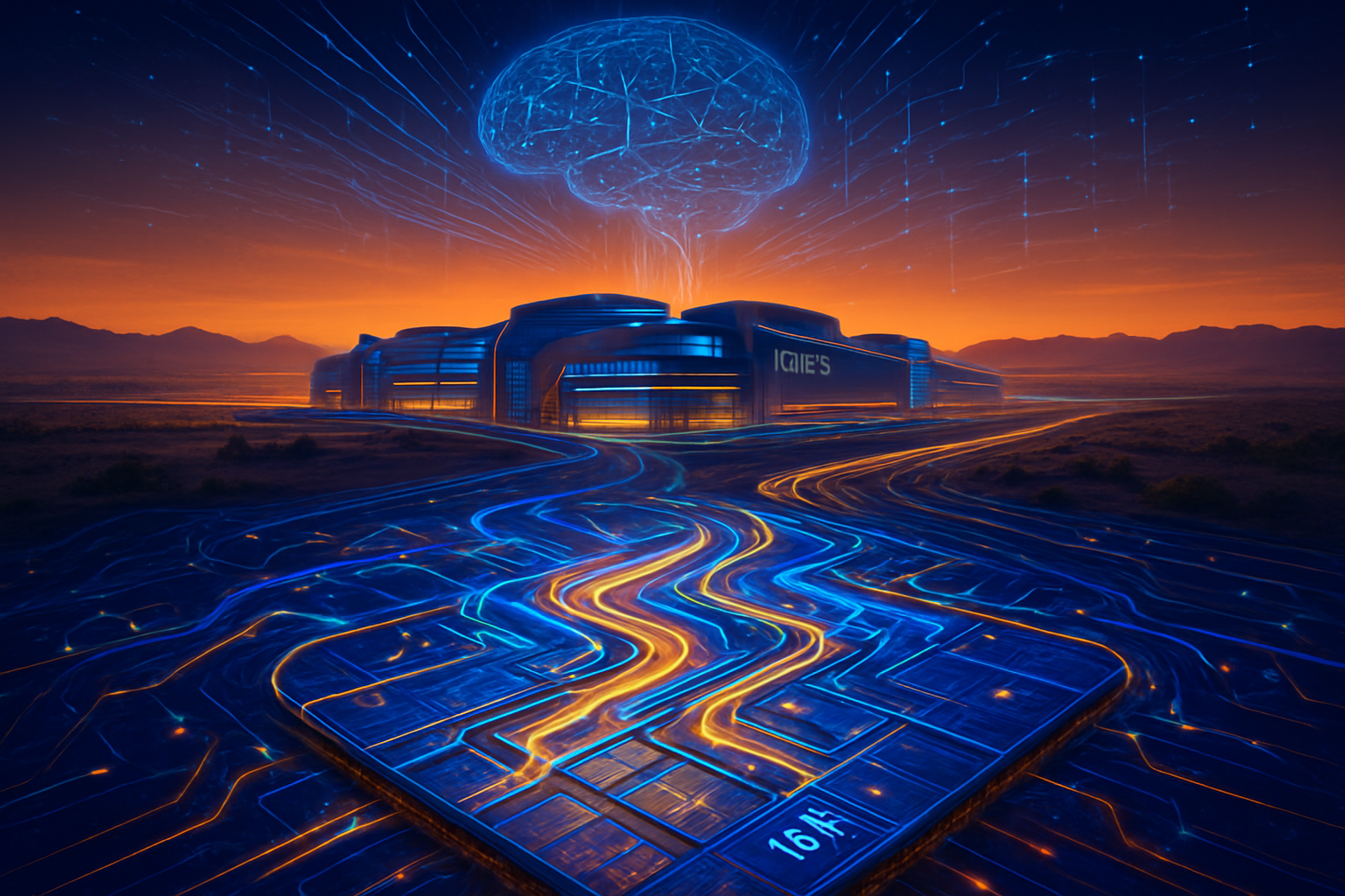
The semiconductor industry has officially entered the "Angstrom Era," marked by the most radical architectural shift in chip manufacturing in over three decades. As of January 5, 2026, the traditional method of routing power through the front of a silicon wafer—a practice that has persisted since the dawn of the integrated circuit—is being abandoned in favor of Backside Power Delivery Networks (BSPDN). This transition is not merely an incremental improvement; it is a fundamental necessity driven by the insatiable energy demands of generative AI and the physical limitations of atomic-scale transistors.
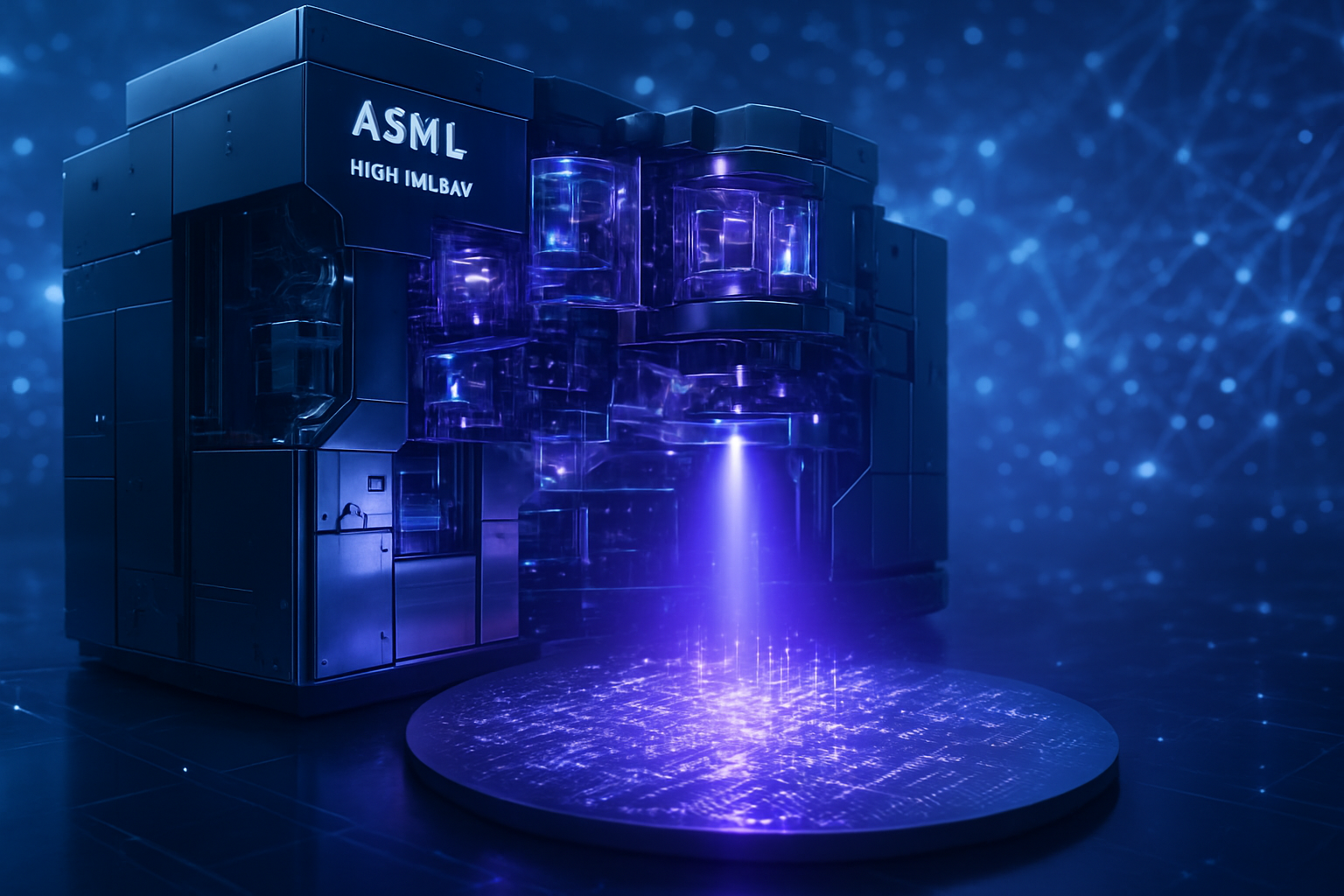
The immediate significance of this shift was underscored today at CES 2026, where Intel Corporation (Nasdaq:INTC) announced the broad market availability of its "Panther Lake" processors, the first consumer-grade chips to utilize high-volume backside power. By decoupling the power delivery from the signal routing, chipmakers are finally solving the "wiring bottleneck" that has plagued the industry. This development ensures that the next generation of AI accelerators, which are now pushing toward 1,000W to 1,500W per module, can receive stable electricity without the catastrophic voltage losses that would have rendered them inefficient or unworkable on older architectures.
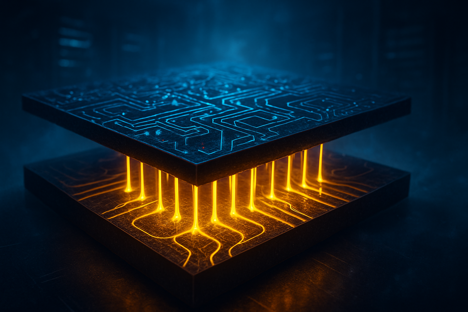
The Technical Divorce: PowerVia vs. Super Power Rail
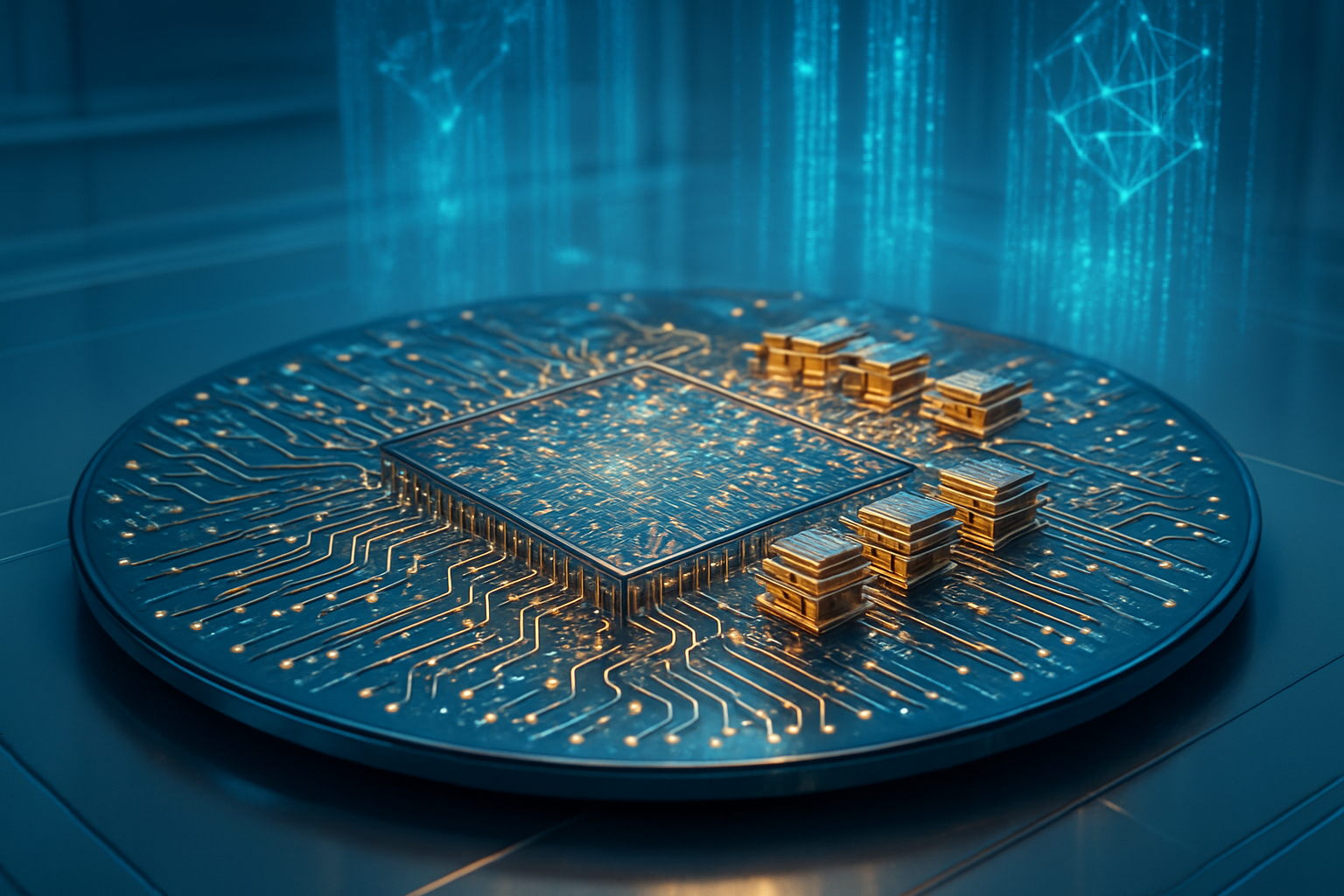
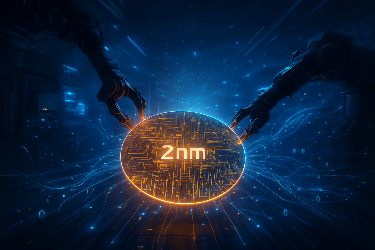
At the heart of this revolution are two competing technical philosophies: Intel’s PowerVia and Taiwan Semiconductor Manufacturing Company’s (NYSE:TSM) Super Power Rail. Historically, both power and data signals were routed through a complex "jungle" of metal layers on top of the transistors. As transistors shrunk to the 2nm and 1.8nm levels, these wires became so thin and crowded that resistance skyrocketed, leading to significant "IR drop"—a phenomenon where voltage decreases as it travels through the chip. BSPDN solves this by moving the power delivery to the reverse side of the wafer, effectively giving the chip two "fronts": one for data and one for energy.
Intel’s PowerVia, debuting in the 18A (1.8nm) process node, utilizes a "nano-TSV" (Through Silicon Via) approach. In this implementation, Intel builds the transistors first, then flips the wafer to create small vertical connections that bridge the backside power layers to the metal layers on the front. This method is considered more manufacturable and has allowed Intel to claim a first-to-market advantage. Early data from Panther Lake production indicates a 30% improvement in voltage droop and a 6% frequency boost at identical power levels compared to traditional front-side delivery. Furthermore, by clearing the "congestion" on the front side, Intel has achieved a staggering 90% standard cell utilization, drastically increasing logic density.
TSMC is taking a more aggressive, albeit delayed, approach with its A16 (1.6nm) node and its "Super Power Rail" technology. Unlike Intel’s nano-TSVs, TSMC’s implementation connects the backside power network directly to the source and drain of the transistors. This direct-contact method is significantly more complex to manufacture, requiring advanced material science to prevent contamination during the bonding process. However, the theoretical payoff is higher: TSMC targets an 8–10% speed improvement and up to a 20% power reduction. While Intel is shipping products today, TSMC is positioning its Super Power Rail as the "refined" version of BSPDN, slated for mass production in the second half of 2026 to power the next generation of high-end AI and mobile silicon.
Strategic Dominance and the AI Arms Race
The shift to backside power has created a new competitive landscape for tech giants and specialized AI labs. Intel’s early lead with 18A and PowerVia is a strategic masterstroke for its Foundry business. By proving the viability of BSPDN in high-volume consumer chips like Panther Lake, Intel is signaling to major fabless customers that it has solved the most difficult scaling challenge of the decade. This puts immense pressure on Samsung Electronics (KRX:005930), which is also racing to implement its own BSPDN version to remain competitive in the logic foundry market.
For AI powerhouses like NVIDIA (Nasdaq:NVDA), the arrival of BSPDN is a lifeline. NVIDIA’s current "Blackwell" architecture and the upcoming "Rubin" platform (scheduled for late 2026) are pushing the limits of data center power infrastructure. With GPUs now drawing well over 1,000W, traditional power delivery would result in massive heat generation and energy waste. By adopting TSMC’s A16 process and Super Power Rail, NVIDIA can ensure that its future Rubin GPUs maintain high clock speeds and reliability even under the extreme workloads required for training trillion-parameter models.
The primary beneficiaries of this development are the "Magnificent Seven" and other hyperscalers who operate massive data centers. Companies like Apple (Nasdaq:AAPL) and Alphabet (Nasdaq:GOOGL) are already reportedly in the queue for TSMC’s A16 capacity. The ability to pack more compute into the same thermal envelope allows these companies to maximize their return on investment for AI infrastructure. Conversely, startups that cannot secure early access to these advanced nodes may find themselves at a performance-per-watt disadvantage, potentially widening the gap between the industry leaders and the rest of the field.
Solving the 1,000W Crisis in the AI Landscape
The broader significance of BSPDN lies in its role as a "force multiplier" for AI scaling laws. For years, experts have worried that we would hit a "power wall" where the energy required to drive a chip would exceed its ability to dissipate heat. BSPDN effectively moves that wall. By thinning the silicon wafer to allow for backside connections, chipmakers also improve the thermal path from the transistors to the cooling solution. This is critical for the 1,000W+ power demands of modern AI accelerators, which would otherwise face severe thermal throttling.
This architectural change mirrors previous industry milestones, such as the transition from planar transistors to FinFETs in the early 2010s. Just as FinFETs allowed the industry to continue scaling despite leakage current issues, BSPDN allows scaling to continue despite resistance issues. However, the transition is not without concerns. The manufacturing process for BSPDN is incredibly delicate; it involves bonding two wafers together with nanometer precision and then grinding one down to a thickness of just a few hundred nanometers. Any misalignment can result in total wafer loss, making yield management the primary challenge for 2026.
Moreover, the environmental impact of this technology is a double-edged sword. While BSPDN makes chips more efficient on a per-calculation basis, the sheer performance gains it enables are likely to encourage even larger, more power-hungry AI clusters. As the industry moves toward 600kW racks for data centers, the efficiency gains of backside power will be essential just to keep the lights on, though they may not necessarily reduce the total global energy footprint of AI.
The Horizon: Beyond 1.6 Nanometers
Looking ahead, the successful deployment of PowerVia and Super Power Rail sets the stage for the sub-1nm era. Industry experts predict that the next logical step after BSPDN will be the integration of "optical interconnects" directly onto the backside of the die. Once the power delivery has been moved to the rear, the front side is theoretically "open" for even more dense signal routing, including light-based data transmission that could eliminate traditional copper wiring altogether for long-range on-chip communication.
In the near term, the focus will shift to how these technologies handle the "Rubin" generation of GPUs and the "Panther Lake" successor, "Nova Lake." The challenge remains the cost: the complexity of backside power adds significant steps to the lithography process, which will likely keep the price of advanced AI silicon high. Analysts expect that by 2027, BSPDN will be the standard for all high-performance computing (HPC) chips, while budget-oriented mobile chips may stick to traditional front-side delivery for another generation to save on manufacturing costs.
A New Foundation for Silicon
The arrival of Backside Power Delivery marks a pivotal moment in the history of computing. It represents a "flipping of the script" in how we design and build the brains of our digital world. By physically separating the two most critical components of a chip—its energy and its information—engineers have unlocked a new path for Moore’s Law to continue into the Angstrom Era.
The key takeaways from this transition are clear: Intel has successfully reclaimed a technical lead by being the first to market with PowerVia, while TSMC is betting on a more complex, higher-performance implementation to maintain its dominance in the AI accelerator market. As we move through 2026, the industry will be watching yield rates and the performance of NVIDIA’s next-generation chips to see which approach yields the best results. For now, the "Power Flip" has successfully averted a scaling crisis, ensuring that the next wave of AI breakthroughs will have the energy they need to come to life.
This content is intended for informational purposes only and represents analysis of current AI developments.
TokenRing AI delivers enterprise-grade solutions for multi-agent AI workflow orchestration, AI-powered development tools, and seamless remote collaboration platforms.
For more information, visit https://www.tokenring.ai/.