In a move that signals a tectonic shift in the global semiconductor landscape, Taiwan Semiconductor Manufacturing Company (NYSE: TSM) has officially commenced mass production of its 2-nanometer (N2) chips at Fab 22 in Kaohsiung. This milestone marks the industry's first large-scale deployment of nanosheet Gate-All-Around (GAA) transistors, a revolutionary architecture that ends the decade-long dominance of FinFET technology. As of January 2, 2026, TSMC stands as the only foundry in the world capable of delivering these ultra-advanced processors at high volumes, effectively resetting the performance and efficiency benchmarks for the entire tech sector.
The transition to the 2nm node is not merely an incremental update; it is a foundational leap required to power the next generation of artificial intelligence, high-performance computing (HPC), and mobile devices. With initial yield rates reportedly reaching an impressive 70%, TSMC has successfully navigated the complexities of the new GAA architecture ahead of its rivals. This achievement cements the company’s role as the primary engine of the AI revolution, as the world's most powerful tech companies scramble to secure their share of this limited, cutting-edge capacity.
The Technical Frontier: Nanosheets and the End of FinFET
The shift from FinFET to Nanosheet GAA (Gate-All-Around) transistors represents the most significant architectural change in chip manufacturing in over ten years. Unlike the outgoing FinFET design, where the gate wraps around three sides of the channel, the N2 process utilizes nanosheets that allow the gate to surround the channel on all four sides. This provides superior control over the electrical current, drastically reducing power leakage and enabling higher performance at lower voltages. Specifically, the N2 process offers a 10% to 15% speed increase at the same power level, or a 25% to 30% reduction in power consumption at the same speed compared to the previous 3nm (N3E) generation.
Beyond the transistor architecture, TSMC has integrated advanced materials and structural innovations to maintain its lead. The N2 node introduces SHPMIM (Super High-Performance Metal-Insulator-Metal) capacitors, which double the capacitance density and reduce resistance by 50% compared to previous designs. These enhancements are critical for power stability in high-frequency AI processors, which often face extreme thermal and electrical demands. Initial reactions from the semiconductor research community have been overwhelmingly positive, with experts noting that TSMC’s ability to hit a 70% yield rate during the early ramp-up phase is a testament to its operational excellence and the maturity of its extreme ultraviolet (EUV) lithography processes.
The epicenter of this production surge is Fab 22 in the Nanzi district of Kaohsiung. Originally planned for older nodes, the facility was pivotally repurposed into a "Gigafab" cluster dedicated to 2nm production. Phase 1 of the facility is now fully operational, utilizing 300mm wafers to churn out the silicon that will define the 2026 product cycle. To keep pace with unprecedented demand, TSMC is already constructing Phases 2 and 3 at the site, part of a broader $28.6 billion capital investment strategy aimed at ensuring its 2nm capacity can eventually reach 100,000 wafers per month by the end of the year.
The "Silicon Elite": Apple, NVIDIA, and the Battle for Capacity
The arrival of 2nm technology has created a widening gap between the "Silicon Elite" and the rest of the industry. Because of the extreme cost—estimated at $30,000 per wafer—only the most profitable tech giants can afford to be early adopters. Apple (NASDAQ: AAPL) has once again secured its position as the lead customer, reportedly reserving over 50% of TSMC’s initial 2nm capacity. This silicon will likely power the A20 Pro chips for the upcoming iPhone 18 series and the M6 family of processors for MacBooks, giving Apple a significant advantage in on-device AI efficiency and battery life.
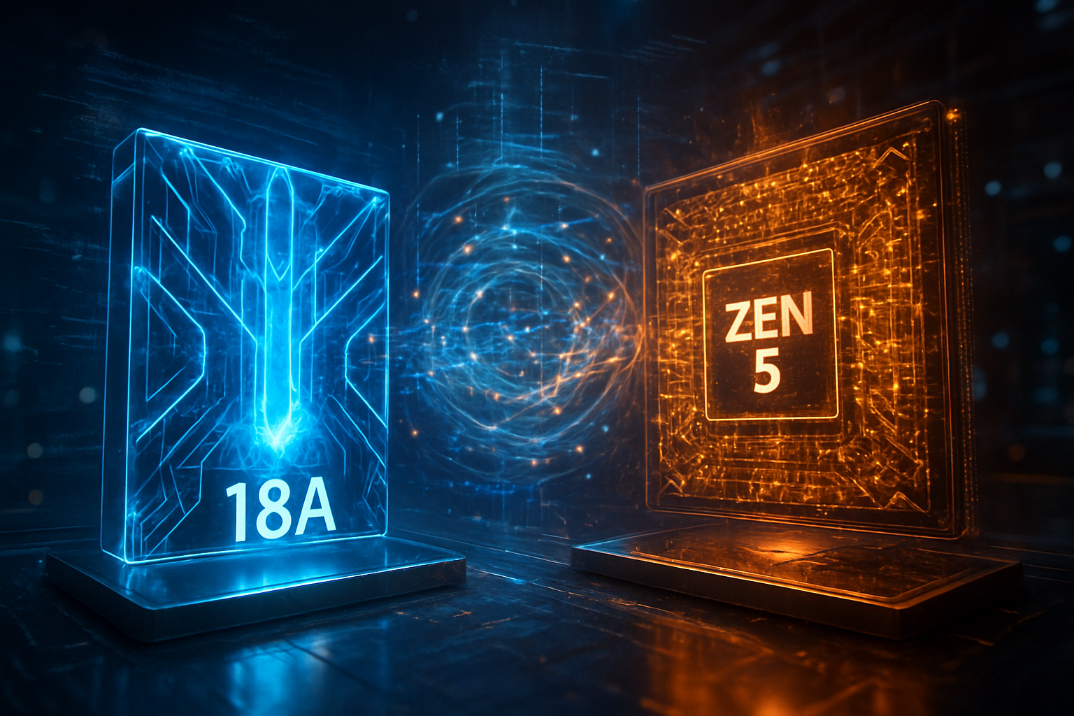
NVIDIA (NASDAQ: NVDA) and AMD (NASDAQ: AMD) have also locked in massive capacity through 2026. For NVIDIA, the move to 2nm is essential for its post-Blackwell AI architectures, such as the rumored "Rubin Ultra" and "Feynman" platforms. These chips will require the density and power efficiency of the N2 node to handle the exponential growth in parameters for Large Language Models (LLMs). AMD is expected to leverage the node for its Zen 6 "Venice" CPUs and MI450 AI accelerators, ensuring it remains competitive in both the data center and consumer markets.
This concentration of advanced manufacturing power creates a strategic moat for these companies. While competitors like Intel (NASDAQ: INTC) and Samsung (KRX: 005930) are racing to stabilize their own GAA processes, TSMC’s proven ability to deliver high-yield 2nm wafers today gives its clients a time-to-market advantage that is difficult to overcome. This dominance has also led to a "structural undersupply" of high-end chips, forcing smaller players to remain on 3nm or 5nm nodes, potentially leading to a bifurcated market where the most advanced AI capabilities are exclusive to a few flagship products.
Powering the AI Landscape: Efficiency and Sovereign Silicon
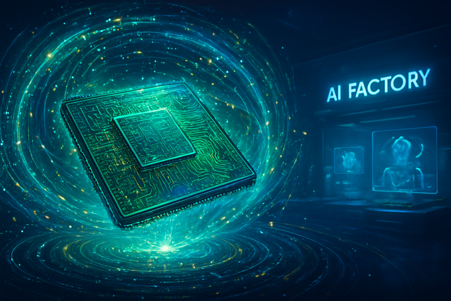
The broader significance of the 2nm breakthrough lies in its impact on the global AI landscape. As AI models become more complex, the energy required to train and run them has become a primary bottleneck for the industry. The 30% power reduction offered by the N2 process is a critical relief valve for data center operators who are struggling with power grid constraints and rising cooling costs. By packing more logic into the same physical footprint with lower energy requirements, 2nm chips allow for more sustainable scaling of AI infrastructure.
Furthermore, the 2nm era marks a turning point for "Edge AI"—the ability to run sophisticated AI models directly on smartphones and laptops rather than in the cloud. The efficiency gains of the N2 node mean that devices can perform more complex tasks, such as real-time video translation or advanced autonomous reasoning, without draining the battery in minutes. This shift toward local processing is also a major win for user privacy and data security, as more information can stay on the device rather than being sent to remote servers.
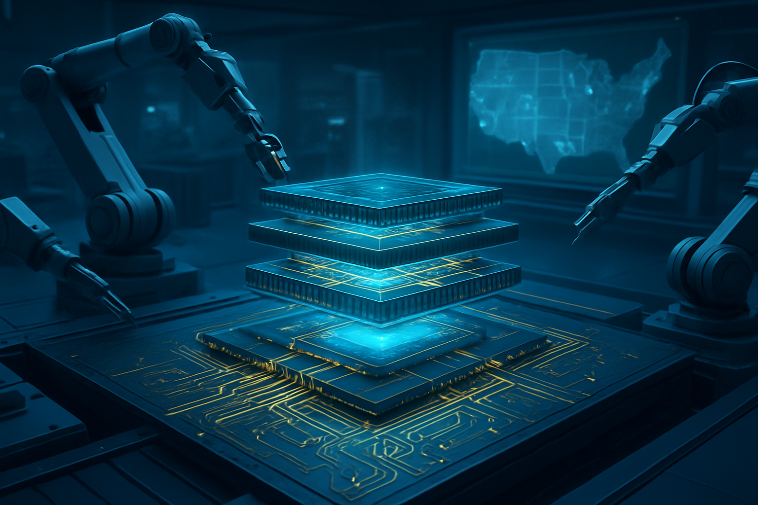
However, the concentration of 2nm production in Taiwan continues to be a point of geopolitical concern. While TSMC is investing $28.6 billion to expand its domestic facilities, it is also feeling the pressure to diversify. The company recently accelerated its plans for Fab 3 in Arizona, moving the start of 2nm and A16 production up to 2027. Despite these efforts, the reality remains that for the foreseeable future, the world’s most advanced artificial intelligence will be physically born in the high-tech corridors of Kaohsiung and Hsinchu, making the stability of the region a matter of global economic security.
The Roadmap Ahead: N2P, A16, and Beyond
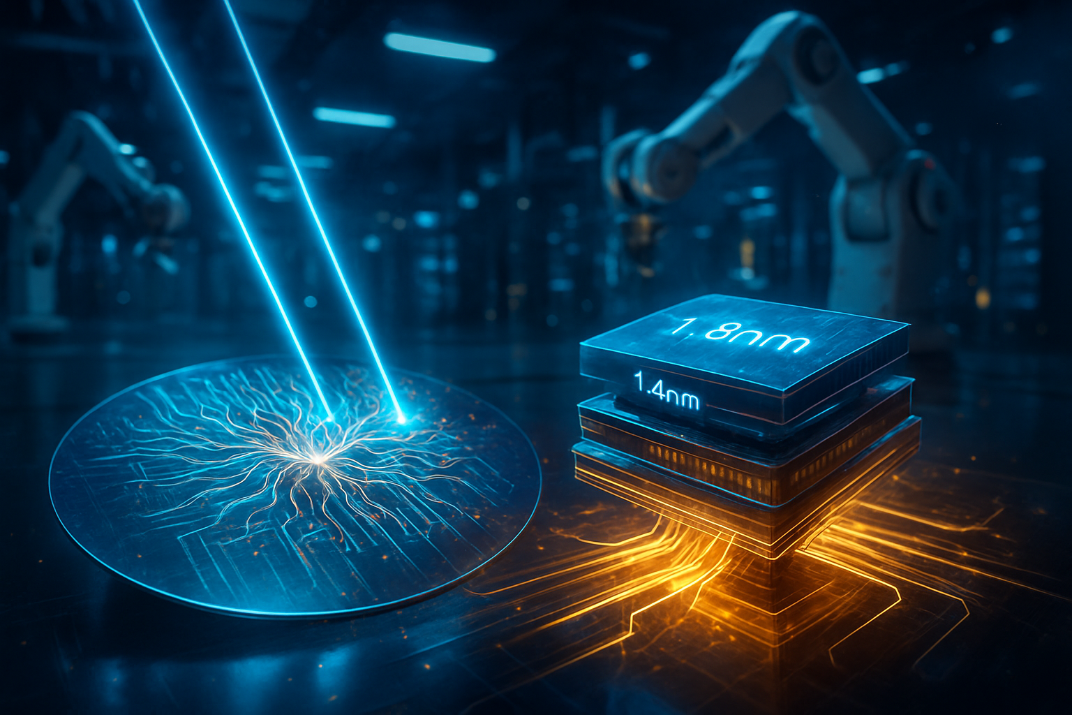
While the industry is just beginning to digest the arrival of 2nm, TSMC’s roadmap is already pointing toward even more ambitious targets. Later in 2026, the company plans to introduce N2P, an enhanced version of the 2nm node that features backside power delivery. This technology moves the power distribution network to the back of the wafer, freeing up space on the front for more signal routing and further improving performance. This will be a crucial bridge to the A16 (1.6nm) node, which is slated for mass production in 2027.
The challenges ahead are primarily centered on the escalating costs of lithography and the physical limits of silicon. As transistors shrink to the size of a few dozen atoms, quantum tunneling and heat dissipation become increasingly difficult to manage. To address this, TSMC is exploring new materials beyond traditional silicon and more advanced 3D packaging techniques, such as CoWoS (Chip-on-Wafer-on-Substrate), which allows multiple 2nm dies to be integrated into a single high-performance package.
Experts predict that the next two years will see a rapid evolution in chip design, as architects move away from "monolithic" chips toward "chiplet" designs that combine 2nm logic with older, more cost-effective nodes for memory and I/O. This modular approach will be essential for managing the skyrocketing costs of design and manufacturing at the leading edge.
A New Chapter in Semiconductor History
TSMC’s successful launch of 2nm mass production at Fab 22 is a watershed moment that defines the beginning of a new era in computing. By successfully transitioning to GAA architecture and securing the world’s most influential tech companies as clients, TSMC has once again proven its ability to execute where others have faltered. The 15% speed boost and 30% power reduction provided by the N2 node will be the primary drivers of AI innovation through the end of the decade.
The significance of this development in AI history cannot be overstated. We are moving from a period of "AI experimentation" to an era of "AI ubiquity," where the hardware is finally catching up to the software's ambitions. As these 2nm chips begin to filter into the market in late 2026, we can expect a surge in the capabilities of everything from autonomous vehicles to personal digital assistants.
In the coming months, the industry will be watching closely for the first third-party benchmarks of the N2 silicon and any updates on the construction of TSMC’s additional 2nm facilities. With the capacity already fully booked, the focus now shifts from "can they build it?" to "how fast can they scale it?" For now, the 2nm crown belongs firmly to TSMC, and the rest of the world is waiting to see what the "Silicon Elite" will build with this unprecedented power.
This content is intended for informational purposes only and represents analysis of current AI developments.
TokenRing AI delivers enterprise-grade solutions for multi-agent AI workflow orchestration, AI-powered development tools, and seamless remote collaboration platforms.
For more information, visit https://www.tokenring.ai/.