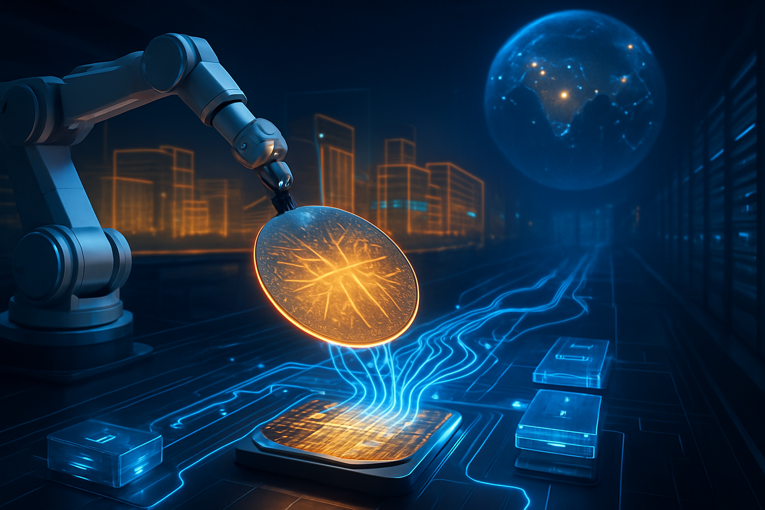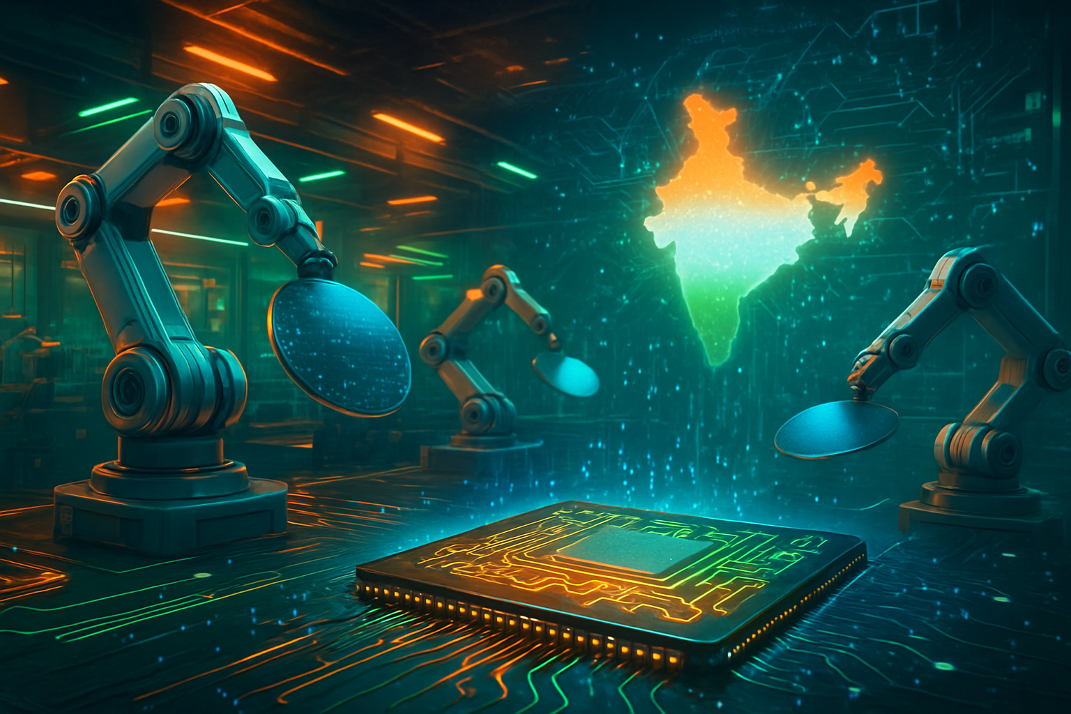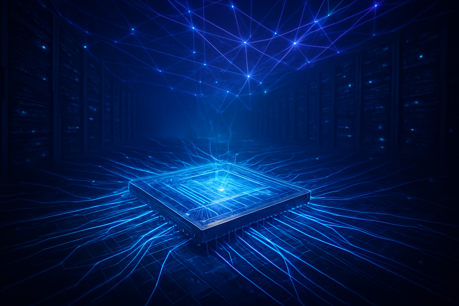
As of January 1, 2026, the global landscape of artificial intelligence hardware has undergone a seismic shift. Huawei has officially announced the wide-scale deployment of its Ascend 950 series AI processors, a milestone that signals the end of the West’s absolute monopoly on high-end compute. By leveraging a sophisticated "EUV-refined" manufacturing process and a vertically integrated stack, Huawei has achieved performance parity with the NVIDIA (NASDAQ: NVDA) H100 and H200 architectures, effectively neutralizing the impact of multi-year export restrictions.
This development marks a pivotal moment in what Beijing terms "Internal Circulation"—a strategic pivot toward total technological self-reliance. The Ascend 950 is not merely a chip; it is the cornerstone of a parallel AI ecosystem. For the first time, Chinese hyperscalers and AI labs have access to domestic silicon that can train the world’s largest Large Language Models (LLMs) without relying on smuggled or depreciated hardware, fundamentally altering the geopolitical balance of the AI arms race.
Technical Mastery: SAQP and the 'Mount Everest' Breakthrough
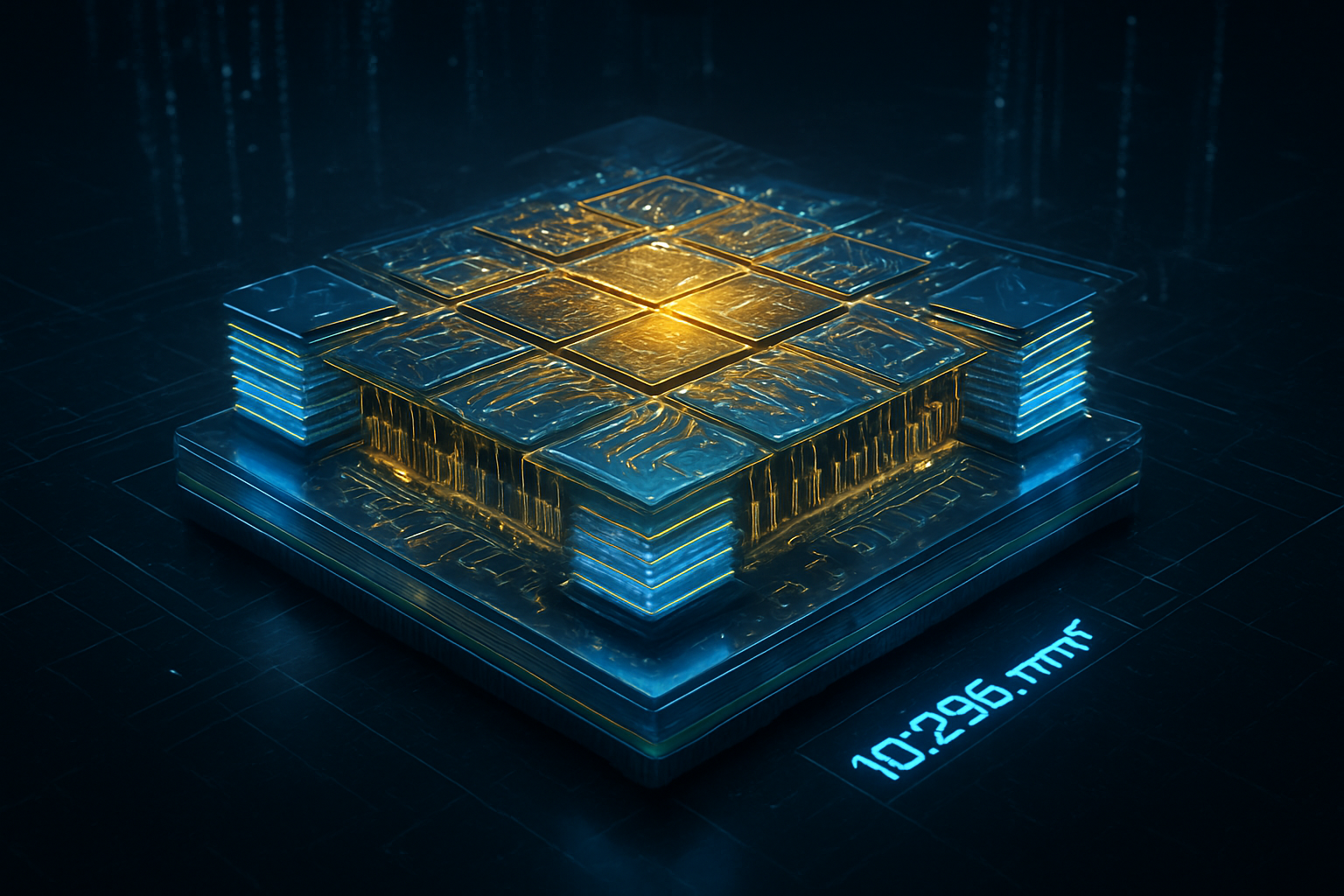
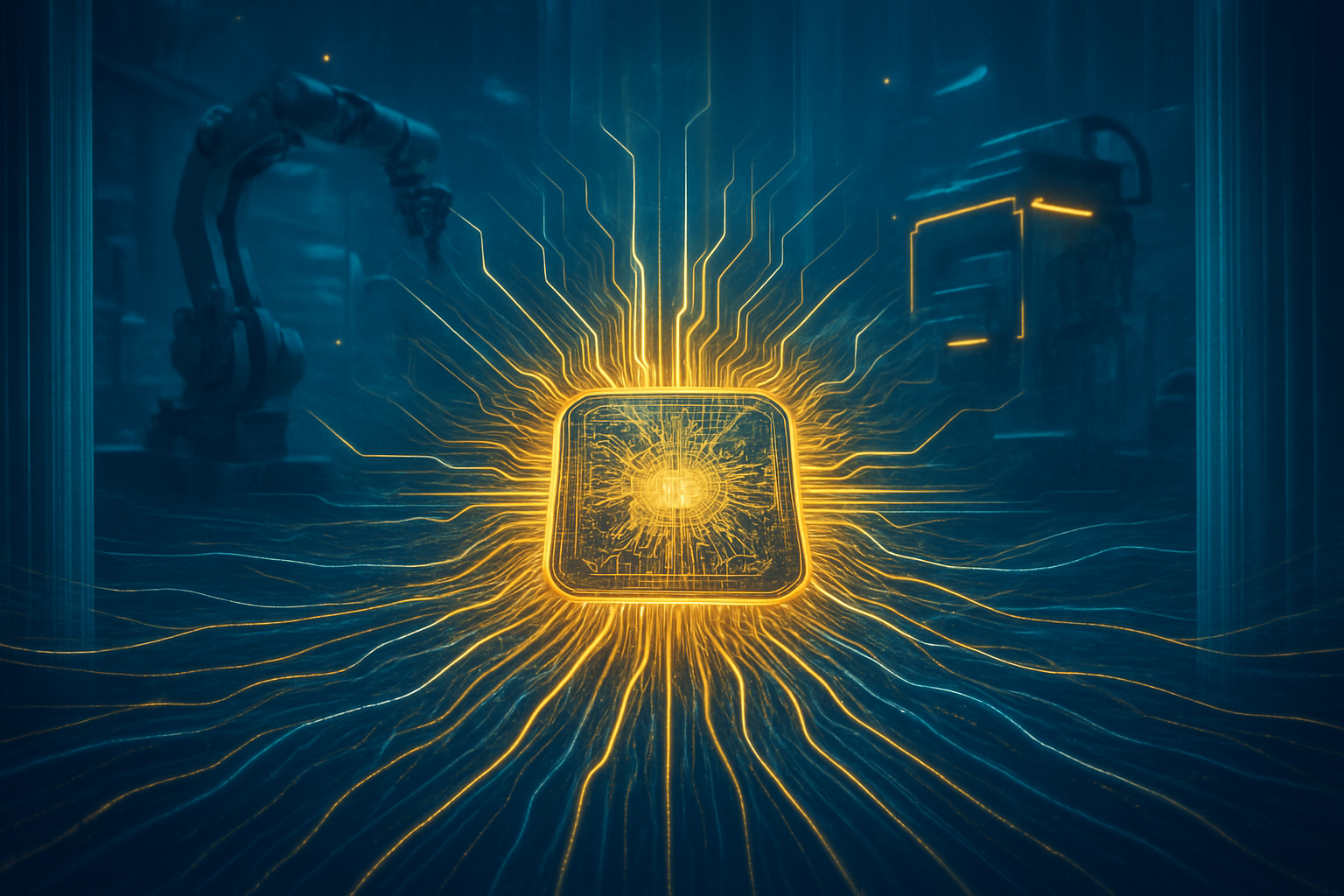
The Ascend 950 series, specifically the 950PR (optimized for inference prefill) and the forthcoming 950DT (dedicated to heavy training), represents a triumph of engineering over constraint. While NVIDIA (NASDAQ: NVDA) utilizes TSMC’s (NYSE: TSM) advanced 4N and 3nm nodes, Huawei and its primary manufacturing partner, Semiconductor Manufacturing International Corporation (SMIC) (HKG: 0981), have achieved 5nm-class densities through a technique known as Self-Aligned Quadruple Patterning (SAQP). This "EUV-refined" process uses existing Deep Ultraviolet (DUV) lithography machines in complex, multi-pass configurations to etch circuits that were previously thought impossible without ASML’s (NASDAQ: ASML) restricted Extreme Ultraviolet (EUV) hardware.
Specifications for the Ascend 950DT are formidable, boasting peak FP8 compute performance of up to 2.0 PetaFLOPS, placing it directly in competition with NVIDIA’s H200. To solve the "memory wall" that has plagued previous domestic chips, Huawei introduced HiZQ 2.0, a proprietary high-bandwidth memory solution that offers 4.0 TB/s of bandwidth, rivaling the HBM3e standards used in the West. This is paired with UnifiedBus, an interconnect fabric capable of 2.0 TB/s, which allows for the seamless clustering of thousands of NPUs into a single logical compute unit.
Initial reactions from the AI research community have been a mix of astonishment and strategic recalibration. Researchers at organizations like DeepSeek and the Beijing Academy of Artificial Intelligence (BAAI) report that the Ascend 950, when paired with Huawei’s CANN 8.0 (Compute Architecture for Neural Networks) software, allows for one-line code conversions from CUDA-based models. This eliminates the "software moat" that has long protected NVIDIA, as the CANN 8.0 compiler can now automatically optimize kernels for the Ascend architecture with minimal performance loss.
Reshaping the Global AI Market
The arrival of the Ascend 950 series creates immediate winners within the Chinese tech sector. Tech giants like Baidu (NASDAQ: BIDU), Tencent (HKG: 0700), and Alibaba (NYSE: BABA) are expected to be the primary beneficiaries, as they can now scale their internal "Ernie" and "Tongyi Qianwen" models on stable, domestic supply chains. For these companies, the Ascend 950 represents more than just performance; it offers "sovereign certainty"—the guarantee that their AI roadmaps cannot be derailed by further changes in U.S. export policy.
For NVIDIA (NASDAQ: NVDA), the implications are stark. While the company remains the global leader with its Blackwell and upcoming Rubin architectures, the "Silicon Curtain" has effectively closed off the world’s second-largest AI market. The competitive pressure is also mounting on other Western firms like Advanced Micro Devices (NASDAQ: AMD) and Intel (NASDAQ: INTC), who now face a Chinese market that is increasingly hostile to foreign silicon. Huawei’s ability to offer a full-stack solution—from the Kunpeng 950 CPUs to the Ascend NPUs and the OceanStor AI storage—positions it as a "one-stop shop" for national-scale AI infrastructure.
Furthermore, the emergence of the Atlas 950 SuperPoD—a massive cluster housing 8,192 Ascend 950 chips—threatens to disrupt the global cloud compute market. Huawei claims this system delivers 6.7x the total computing power of current Western-designed clusters of similar scale. This strategic advantage allows Chinese startups to train models with trillions of parameters at a fraction of the cost previously incurred when renting "sanction-compliant" GPUs from international cloud providers.
The Global Reshoring Perspective: A New Industrial Era
From the perspective of China’s "Global Reshoring" strategy, the Ascend 950 is the ultimate proof of concept for industrial "Internal Circulation." While the West has focused on reshoring to secure jobs and supply chains, China’s version is an existential mandate to decouple from Western IP entirely. The success of the "EUV-refined" process suggests that the technological "ceiling" imposed by sanctions was more of a "hurdle" that Chinese engineers have now cleared through sheer iterative volume and state-backed capital.
This shift mirrors previous industrial milestones, such as the development of China’s high-speed rail or its dominance in the EV battery market. It signifies a transition from a globalized, interdependent tech world to a bifurcated one. The "Silicon Curtain" is now a physical reality, with two distinct stacks of hardware, software, and standards. This raises significant concerns about global interoperability and the potential for a "cold war" in AI safety and alignment standards, as the two ecosystems may develop along radically different ethical and technical trajectories.
Critics and skeptics point out that the "EUV-refined" DUV process is inherently less efficient, with lower yields and higher power consumption than true EUV manufacturing. However, in the context of national security and strategic autonomy, these economic inefficiencies are secondary to the primary goal of compute sovereignty. The Ascend 950 proves that a nation-state with sufficient resources can "brute-force" its way into the top tier of semiconductor design, regardless of international restrictions.
The Horizon: 3nm and Beyond
Looking ahead to the remainder of 2026 and 2027, Huawei’s roadmap shows no signs of slowing. Rumors of the Ascend 960 suggest that Huawei is already testing prototypes that utilize a fully domestic EUV lithography system developed under the secretive "Project Mount Everest." If successful, this would move China into the 3nm frontier by 2027, potentially reaching parity with NVIDIA’s next-generation architectures ahead of schedule.
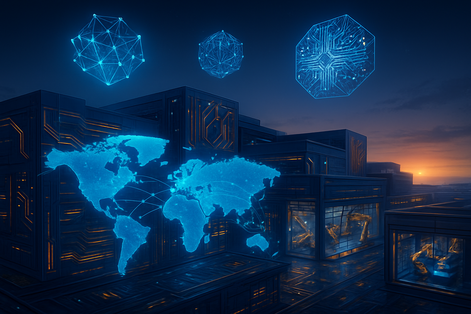
The next major challenge for the Ascend ecosystem will be the expansion of its developer base outside of China. While domestic adoption is guaranteed, Huawei is expected to aggressively market the Ascend 950 to "Global South" nations looking for an alternative to Western technology stacks. We can expect to see "AI Sovereignty" packages—bundled hardware, software, and training services—offered to countries in Southeast Asia, the Middle East, and Africa, further extending the reach of the Chinese AI ecosystem.
A New Chapter in AI History
The launch of the Ascend 950 series will likely be remembered as the moment the "unipolar" era of AI compute ended. Huawei has demonstrated that through a combination of custom silicon design, innovative manufacturing workarounds, and a massive vertically integrated stack, it is possible to rival the world’s most advanced technology firms under the most stringent constraints.
Key takeaways from this development include the resilience of the Chinese semiconductor supply chain and the diminishing returns of export controls on mature-node and refined-node technologies. As we move into 2026, the industry must watch for the first benchmarks of LLMs trained entirely on Ascend 950 clusters. The performance of these models will be the final metric of success for Huawei’s ambitious leap into the future of AI.
This content is intended for informational purposes only and represents analysis of current AI developments.
TokenRing AI delivers enterprise-grade solutions for multi-agent AI workflow orchestration, AI-powered development tools, and seamless remote collaboration platforms.
For more information, visit https://www.tokenring.ai/.