Tag: Semiconductors

  • Samsung Stages Massive AI Comeback as HBM4 Passes NVIDIA Verification for Rubin Platform

    Samsung Stages Massive AI Comeback as HBM4 Passes NVIDIA Verification for Rubin Platform

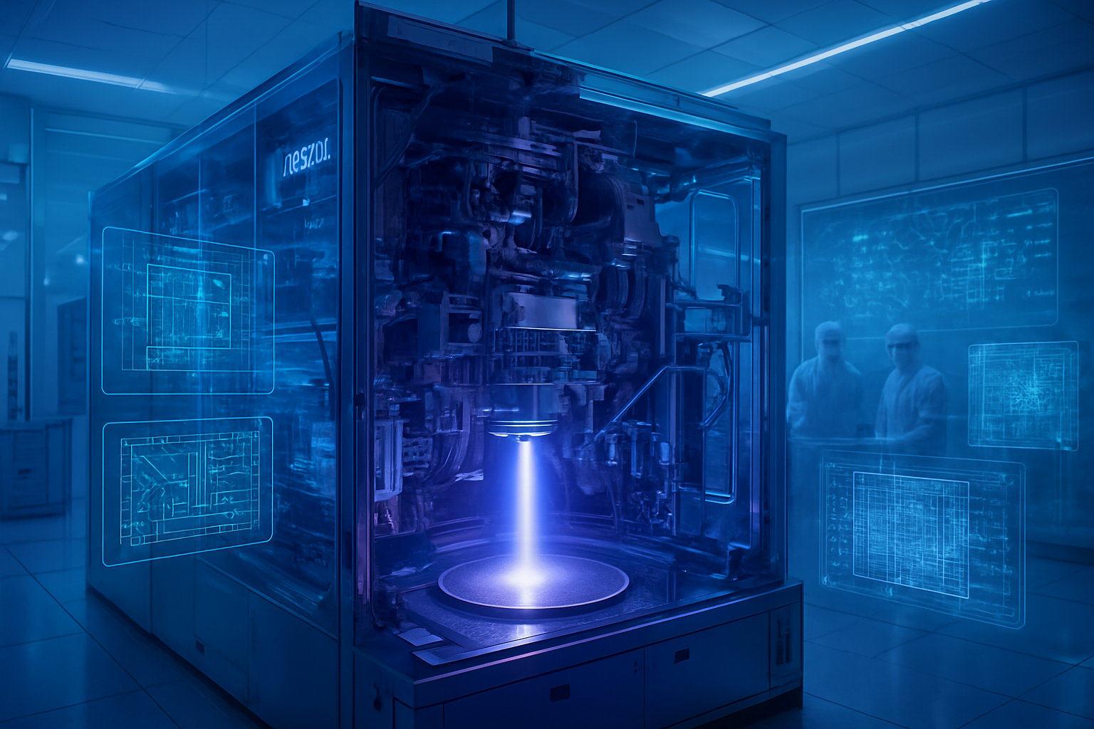
    In a pivotal shift for the global semiconductor landscape, Samsung Electronics (KRX: 005930) has officially cleared final verification for its sixth-generation high-bandwidth memory, known as HBM4, for use in NVIDIA's (NASDAQ: NVDA) upcoming "Rubin" AI platform. This milestone, achieved in late January 2026, marks a dramatic resurgence for the South Korean tech giant after it spent much of the previous two years trailing behind competitors in the high-stakes AI memory race. With mass production scheduled to commence this month, Samsung has secured its position as a primary supplier for the hardware that will power the next era of generative AI.

    The verification success is more than just a technical win; it is a strategic lifeline for the global AI supply chain. For over a year, NVIDIA and other AI chipmakers have faced bottlenecks due to the limited production capacity of previous-generation HBM3e memory. By bringing Samsung's HBM4 online ahead of the official Rubin volume rollout in the second half of 2026, NVIDIA has effectively diversified its supply base, reducing its reliance on a single provider and ensuring that the massive compute demands of future large language models (LLMs) can be met without the crippling shortages that characterized the Blackwell era.

    The Technical Leap: 1c DRAM and the Turnkey Advantage

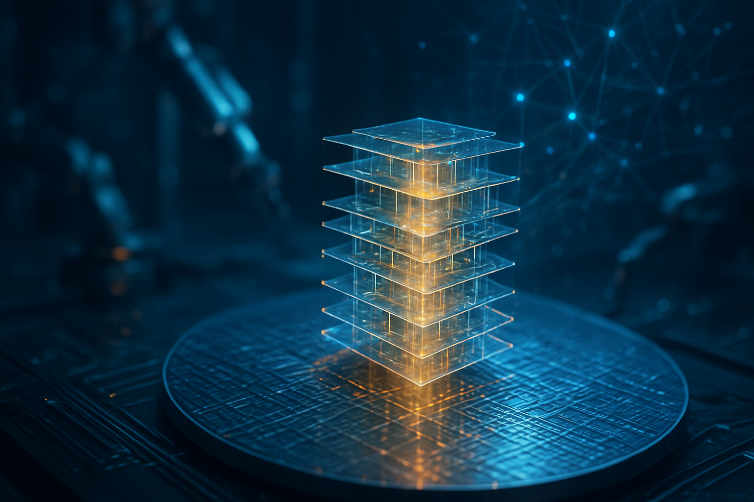
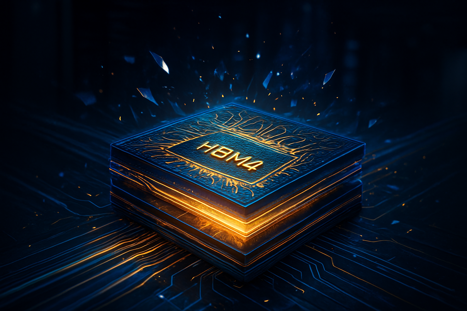
    Samsung’s HBM4 represents a fundamental departure from the architecture of its predecessors. Unlike HBM3e, which focused primarily on incremental speed increases, HBM4 moves toward a logic-integrated architecture. Samsung’s specific implementation features 12-layer (12-Hi) stacks with a capacity of 36GB per stack. These modules utilize Samsung’s sixth-generation 10nm-class (1c) DRAM process, which reportedly offers a 20% improvement in power efficiency—a critical factor for data centers already struggling with the immense thermal and electrical requirements of modern AI clusters.

    A key differentiator in Samsung's approach is its "turnkey" manufacturing model. While competitors often rely on external foundries for the base logic die, Samsung has leveraged its internal 4nm foundry process to produce the logic die that sits at the bottom of the HBM stack. This vertical integration allows for tighter coupling between the memory and logic components, reducing latency and optimizing the power-performance ratio. During testing, Samsung’s HBM4 achieved data transfer rates of 11.7 Gbps per pin, surpassing the JEDEC standard and providing a total bandwidth exceeding 2.8 TB/s per stack.

    Industry experts have noted that this "one-roof" solution—encompassing DRAM production, logic die manufacturing, and advanced 2.5D/3D packaging—gives Samsung a unique advantage in shortening lead times. Initial reactions from the AI research community suggest that the integration of HBM4 into NVIDIA’s Rubin platform will enable a "memory-first" architecture, where the GPU is less constrained by data transfer bottlenecks, allowing for the training of models with trillions of parameters in significantly shorter timeframes.

    Reshaping the Competitive Landscape: The Three-Way War

    The verification of Samsung’s HBM4 has ignited a fierce three-way battle for dominance in the high-performance memory market. For the past two years, SK Hynix (KRX: 000660) held a commanding lead, having been the exclusive provider for much of NVIDIA’s early AI hardware. However, Samsung’s early leap into HBM4 mass production in February 2026 threatens that hegemony. While SK Hynix remains a formidable leader with its own HBM4 units expected later this year, the market share is rapidly shifting. Analysts estimate that Samsung could capture up to 30% of the HBM4 market by the end of 2026, up from its lower double-digit share during the HBM3e cycle.

    For NVIDIA, the inclusion of Samsung is a tactical masterpiece. It places the GPU kingmaker in a position of maximum leverage over its suppliers, which also include Micron (NASDAQ: MU). Micron has been aggressively expanding its capacity with a $20 billion capital expenditure plan, aiming for a 20% market share by late 2026. This competitive pressure is expected to drive down the premiums associated with HBM, potentially lowering the overall cost of AI infrastructure for hyperscalers and startups alike.

    Furthermore, the competitive dynamics are forcing new alliances. SK Hynix has deepened its partnership with Taiwan Semiconductor Manufacturing Co. (NYSE: TSM) to co-develop the logic dies for its version of HBM4, creating a "One-Team" front against Samsung’s internal foundry model. This divergence in strategy—integrated vs. collaborative—will be the defining theme of the semiconductor industry over the next 24 months as companies race to provide the most efficient "Custom HBM" solutions tailored to specific AI workloads.

    Breaking the Memory Wall in the Rubin Era

    The broader significance of Samsung’s HBM4 verification lies in its role as the engine for the NVIDIA Rubin architecture. Rubin is designed as a "sovereign AI" powerhouse, featuring the Vera CPU and Rubin GPU built on a 3nm process. Each Rubin GPU is expected to utilize eight stacks of HBM4, providing a staggering 288GB of high-speed memory per chip. This massive increase in memory capacity and bandwidth is the primary weapon in the industry's fight against the "Memory Wall"—the point where processor performance outstrips the ability of memory to feed it data.

    In the global AI landscape, this breakthrough facilitates the move toward more complex, multi-modal AI systems that can process video, audio, and text simultaneously in real-time. It also addresses growing concerns regarding energy consumption. By utilizing the 1c DRAM process and advanced packaging, HBM4 delivers more "work per watt," which is essential for the sustainability of the massive data centers being planned by tech giants.

    Comparisons are already being drawn to the 2023 transition to HBM3, which enabled the first wave of the generative AI boom. However, the shift to HBM4 is seen as more transformative because it signals the end of generic memory. We are entering an era of "Custom HBM," where the memory is no longer just a storage bin for data but an active participant in the compute process, with logic dies optimized for specific algorithms.

    Future Horizons: 16-Layer Stacks and Hybrid Bonding

    Looking ahead, the roadmap for HBM4 is already extending toward even denser configurations. While the current 12-layer stacks are the initial focus, Samsung is already conducting pilot runs for 16-layer (16-Hi) HBM4, which would increase capacity to 48GB or 64GB per stack. These future iterations are expected to employ "hybrid bonding" technology, a manufacturing technique that eliminates the need for traditional solder bumps between layers, allowing for thinner stacks and even higher interconnect density.

    Experts predict that by 2027, the industry will see the first "HBM-on-Chip" designs, where the memory is bonded directly on top of the processor logic rather than adjacent to it. Challenges remain, particularly regarding the yield rates of these ultra-complex 3D structures and the precision required for hybrid bonding. However, the successful verification for the Rubin platform suggests that these hurdles are being cleared faster than many anticipated. Near-term applications will likely focus on high-end scientific simulation and the training of the next generation of "frontier models" by organizations like OpenAI and Anthropic.

    A New Chapter for AI infrastructure

    The successful verification of Samsung’s HBM4 for NVIDIA’s Rubin platform marks a definitive end to Samsung’s period of playing catch-up. By aligning its 1c DRAM and internal foundry capabilities, Samsung has not only secured its financial future in the AI era but has also provided the industry with the diversity of supply needed to maintain the current pace of AI innovation. The announcement sets the stage for a blockbuster GTC 2026 in March, where NVIDIA is expected to showcase the first live demonstrations of Rubin silicon powered by these new memory stacks.

    As we move into the second half of 2026, the industry will be watching closely to see how quickly Samsung can scale its production to meet the expected deluge of orders. The "Memory Wall" has been pushed back once again, and with it, the boundaries of what artificial intelligence can achieve. The next few months will be critical as the first Rubin-based systems begin their journey from the assembly line to the world’s most powerful data centers, officially ushering in the sixth generation of high-bandwidth memory.


    This content is intended for informational purposes only and represents analysis of current AI developments.

    TokenRing AI delivers enterprise-grade solutions for multi-agent AI workflow orchestration, AI-powered development tools, and seamless remote collaboration platforms.
    For more information, visit https://www.tokenring.ai/.

  • TSMC’s $165 Billion ‘Megafab’ Vision: How the Phoenix Expansion Secures the Future of AI Silicon

    TSMC’s $165 Billion ‘Megafab’ Vision: How the Phoenix Expansion Secures the Future of AI Silicon

    In a move that cements the American Southwest as the next global epicenter for high-performance computing, Taiwan Semiconductor Manufacturing Company (NYSE: TSM) has successfully bid $197.25 million to acquire 902 acres of state trust land in North Phoenix. This strategic acquisition, finalized in January 2026, nearly doubles the company's footprint in Arizona to over 2,000 acres, providing the geographic foundation for what is now being called a "Megafab Cluster." The expansion is not merely about physical space; it represents a monumental shift in the semiconductor landscape, as TSMC pivots to integrate advanced packaging facilities directly onto U.S. soil to meet the insatiable demand for AI hardware.

    This land purchase is the cornerstone of a broader $165 billion investment plan that has grown significantly since the initial 2020 announcement. By securing this contiguous plot near the Loop 303 and Interstate 17 interchange, TSMC is preparing to scale its operations to potentially six fabrication plants (Fabs 1-6). More importantly, the company has signaled a shift in strategy by exploring the repurposing of land originally intended for its sixth fab to house a dedicated advanced packaging facility. This move aims to bring "CoWoS" (Chip on Wafer on Substrate) technology—the secret sauce behind the world’s most powerful AI accelerators—to the United States, effectively creating a self-sustaining, end-to-end manufacturing ecosystem.

    Engineering the Future of 1.6nm Nodes and Domestic CoWoS

    The technical roadmap for the Arizona Megafab Cluster is aggressive, positioning the Phoenix site at the bleeding edge of semiconductor physics. While Fab 1 is already operational, churning out 4nm and 5nm chips, and Fab 2 is prepping for 3nm mass production by the second half of 2027, the focus is now shifting to Fab 3. This facility is slated to pioneer 2nm and the highly anticipated "A16" (1.6nm) process nodes by 2029. These nodes utilize gate-all-around (GAA) transistor architectures and backside power delivery, features essential for the energy-efficiency requirements of the next generation of generative AI models.

    The inclusion of an in-house advanced packaging facility is perhaps the most significant technical advancement for the Arizona site. Previously, even "Made in USA" wafers had to be shipped back to Taiwan for final assembly using TSMC’s proprietary CoWoS technology. By establishing domestic advanced packaging, TSMC can perform high-density interconnecting of logic and memory chips (like HBM4) locally. This differs from previous approaches by eliminating the logistical bottleneck and geopolitical risk of trans-Pacific shipping during the final stages of production. Industry experts note that this domestic packaging capability is the final piece of the puzzle for a resilient, high-volume supply chain for AI hardware.

    Initial reactions from the AI research community have been overwhelmingly positive, particularly regarding the A16 node. The ability to manufacture 1.6nm chips with domestic packaging is seen as a "holy grail" for latency-sensitive AI applications. Dr. Sarah Chen, a leading semiconductor analyst, noted that "the proximity of advanced logic and advanced packaging on a single campus in Phoenix will likely reduce production cycle times by weeks, providing a critical competitive edge to Western tech giants."

    Reshaping the AI Hardware Hierarchy: Winners and Losers

    This expansion creates a massive strategic advantage for TSMC’s primary customers, most notably Nvidia (NASDAQ: NVDA) and Apple (NASDAQ: AAPL). Nvidia, which is projected to become TSMC’s largest customer by revenue in 2026, stands to benefit the most. With the "Blackwell" and "Rubin" series of AI accelerators requiring advanced CoWoS packaging, the ability to manufacture and assemble these units entirely within Arizona allows Nvidia to secure its supply chain against potential disruptions in the Taiwan Strait. This move effectively de-risks the production of the world’s most sought-after AI silicon.

    For Apple, the accelerated timeline for 3nm production in Fab 2 and the proximity of Amkor Technology (NASDAQ: AMKR)—which is building a $7 billion packaging facility nearby—ensures a steady supply of A-series and M-series chips for the iPhone and Mac. Meanwhile, competitors like Intel (NASDAQ: INTC) and Samsung (KRX: 005930) face increased pressure. Intel, which has been aggressively marketing its "Intel Foundry" services, now faces a direct domestic challenge from TSMC at the most advanced nodes. While Intel is also expanding its presence in Arizona and Ohio, TSMC’s "Megafab" scale and its established ecosystem of tool and chemical suppliers in the Phoenix area provide a formidable lead in operational efficiency.

    The market positioning of Advanced Micro Devices (NASDAQ: AMD) is also strengthened by this expansion. As a major TSMC partner, AMD can leverage the Arizona cluster for its EPYC processors and Instinct AI accelerators. The strategic advantage for these companies is clear: the Arizona expansion provides "Silicon Shield" protection while maintaining the performance lead that only TSMC’s process nodes can currently provide. Startups in the custom AI silicon space also stand to benefit, as the increased domestic capacity may lower the barrier to entry for smaller-volume, high-performance chip designs.

    Geopolitics, The "Silicon Pact," and the AI Landscape

    The Arizona expansion must be viewed through the lens of the broader AI arms race and global geopolitics. The project has been bolstered by the "2026 US-Taiwan Trade and Investment Agreement," also known as the "Silicon Pact," signed in January 2026. This historic agreement saw Taiwanese companies commit to $250 billion in U.S. investment in exchange for tariff relief—reducing general rates from 20% to 15%—and duty-free export provisions for semiconductors. This economic framework bridges the cost gap between manufacturing in Phoenix versus Hsinchu, making the Arizona operation financially viable for the long term.

    However, the expansion is not without its concerns. The sheer scale of the 2,000-acre campus has raised questions about the environmental impact on the arid Arizona landscape, particularly regarding water usage and power consumption. TSMC has addressed these concerns by committing to industry-leading water reclamation rates, aiming to recycle over 90% of the water used in its facilities. Furthermore, the expansion highlights the "brain drain" concerns in Taiwan, as thousands of highly skilled engineers are relocated to the U.S. to oversee the complex ramp-up of sub-2nm nodes.

    Comparatively, this milestone is being likened to the establishment of the original Silicon Valley. While the 20th century was defined by software clusters, the mid-21st century is being defined by "Hard-AI Clusters." The Phoenix Megafab is the physical manifestation of the transition from the "Cloud Era" to the "Physical AI Era," where the proximity of energy, land, and advanced lithography determines which nations lead in artificial intelligence.

    The Road to Sub-1nm and Beyond

    Looking ahead, the near-term focus will be the successful installation of High-NA EUV (Extreme Ultraviolet) lithography machines in Fab 3. These machines, costing upwards of $350 million each, are essential for reaching the 1.6nm and eventual sub-1nm thresholds. By 2028, experts expect to see the first pilot runs of "Angstrom-era" chips in Phoenix, a milestone that would have been unthinkable for U.S.-based manufacturing just a decade ago.

    The potential applications on the horizon are vast. From on-device generative AI that operates with the complexity of today's massive data centers to autonomous systems that require instantaneous local processing, the chips produced in Arizona will power the next decade of innovation. However, the primary challenge remains the workforce. TSMC and the state of Arizona are investing heavily in community college programs and university partnerships to train the estimated 12,000 highly skilled technicians and engineers needed to staff the full six-fab cluster.

    A New Chapter in Industrial History

    TSMC's $197 million land purchase and the subsequent $165 billion "Megafab Cluster" represent a turning point in the history of technology. This development marks the end of the era where the most advanced manufacturing was concentrated in a single, geographically vulnerable location. By bringing 1.6nm production and CoWoS advanced packaging to Arizona, TSMC has effectively decoupled the future of AI from the immediate geopolitical uncertainties of the Pacific.

    The significance of this development in AI history cannot be overstated. We are witnessing the birth of a domestic high-tech industrial base that will serve as the backbone for the AI economy for the next thirty years. In the coming weeks and months, watch for announcements regarding additional supply chain partners—chemical suppliers, tool makers, and testing firms—flocking to the Phoenix area, further solidifying the "Silicon Desert" as the most critical tech corridor on the planet.


    This content is intended for informational purposes only and represents analysis of current AI developments.

    TokenRing AI delivers enterprise-grade solutions for multi-agent AI workflow orchestration, AI-powered development tools, and seamless remote collaboration platforms.
    For more information, visit https://www.tokenring.ai/.

  • The Bespoke Silicon Revolution: Broadcom’s $50 Billion Surge Redefines the AI Hardware Landscape

    The Bespoke Silicon Revolution: Broadcom’s $50 Billion Surge Redefines the AI Hardware Landscape

    As of early 2026, the artificial intelligence industry has reached a critical inflection point where generic hardware is no longer enough to satisfy the hunger of multi-trillion parameter models. Leading this fundamental shift is Broadcom Inc. (NASDAQ: AVGO), which has successfully transitioned from a diversified networking giant into the primary architect of the custom AI silicon era. By positioning itself as the indispensable partner for hyperscalers like Google and Meta, and now the primary engine behind OpenAI’s hardware ambitions, Broadcom is witnessing a historic surge in revenue that is reshaping the semiconductor market.

    The numbers tell a story of rapid, unprecedented dominance. After closing a blockbuster fiscal year 2025 with $20 billion in AI-related revenue, Broadcom is now on track to more than double that figure in 2026, with projections soaring toward the $50 billion mark. With an AI order backlog currently sitting at a staggering $73 billion, the company has effectively bifurcated the AI chip market: while Nvidia Corp. (NASDAQ: NVDA) remains the king of general-purpose training, Broadcom has become the undisputed sovereign of custom Application-Specific Integrated Circuits (ASICs), providing the "bespoke compute" that allows the world’s largest tech companies to bypass the "Nvidia tax" and build more efficient, specialized data centers.

    Engineering the Architecture of Sovereign AI

    The core of Broadcom’s technical advantage lies in its ability to co-design chips that strip away the silicon "cruft" found in general-purpose GPUs. While Nvidia’s Blackwell and newly released Rubin platforms must support a vast array of legacy applications and diverse workloads, Broadcom’s ASICs—such as Google’s (NASDAQ: GOOGL) TPU v7 and Meta Platforms' (NASDAQ: META) MTIA v4—are laser-focused on the specific mathematical operations required for Large Language Models (LLMs). This specialization allows for a 30% to 50% improvement in performance-per-watt compared to off-the-shelf GPUs. In an era where data center power limits have become the primary bottleneck for AI scaling, this energy efficiency is not just a cost-saving measure; it is a strategic necessity.

    The technical specifications of these new accelerators are formidable. The Google TPU v7 (codenamed "Ironwood"), built on a 3nm process, is optimized specifically for the latest Gemini 2.0 and 3.0 models. Meanwhile, the Meta MTIA v4 (Santa Barbara), currently deploying across Meta’s massive fleet of servers, features liquid-cooled rack integration and advanced 3D Torus networking topologies. This architecture allows companies to cluster over 9,000 chips into a single unified "Superpod" with minimal latency, far exceeding the scale of traditional GPU clusters. Broadcom provides the critical intellectual property—including high-speed SerDes, HBM controllers, and networking interconnects—while leveraging its deep partnership with Taiwan Semiconductor Manufacturing Co. (NYSE: TSM) for advanced packaging.

    Shifting the Competitive Power Balance

    This surge in custom silicon is fundamentally altering the power dynamics among tech giants. By developing their own chips through Broadcom, companies like Meta and Google are achieving a level of vertical integration that provides a significant competitive moat. For these hyperscalers, the shift to ASICs represents a "decoupling" from the supply chain volatility and high margins associated with third-party GPU vendors. It allows them to optimize their entire stack—from the underlying silicon and networking to the AI models themselves—resulting in a lower Total Cost of Ownership (TCO) that startups and smaller labs simply cannot match.

    The market is also witnessing the emergence of a "second tier" of custom silicon providers, most notably Marvell Technology Inc. (NASDAQ: MRVL), which has secured its own landmark deals with Amazon and Microsoft. However, Broadcom remains the dominant force, controlling roughly 65% of the custom AI ASIC market. This positioning has made Broadcom a "proxy" for the overall health of the AI infrastructure sector. As OpenAI officially joins Broadcom’s customer roster with a multi-billion dollar project to build its own "sovereignty" chip, the company’s role has evolved from a supplier to a strategic kingmaker. OpenAI’s move to internal silicon, specifically designed to run its high-intensity "reasoning" models like the o1-series, signals that the industry's heaviest hitters are no longer content with being customers—they want to be architects.

    The Broader Implications for the AI Landscape

    Broadcom’s success reflects a broader trend toward the fragmentation of the AI hardware landscape. We are moving away from a world of "one size fits all" compute and toward a heterogeneous environment where different chips are tuned for specific tasks: training, inference, or reasoning. This shift mimics the evolution of the mobile industry, where Apple’s move to internal silicon eventually redefined the performance benchmarks for the entire smartphone market. By enabling Google, Meta, and OpenAI to do the same for AI, Broadcom is accelerating a future where the most advanced AI capabilities are tied directly to proprietary hardware.

    However, this trend toward custom silicon also raises concerns about market consolidation. As the barrier to entry for high-end AI moves from "buying GPUs" to "designing multi-billion dollar custom chips," the gap between the "Big Five" hyperscalers and the rest of the industry may become an unbridgeable chasm. Furthermore, the reliance on a few key players—specifically Broadcom for design and TSMC for fabrication—creates new points of failure in the global AI supply chain. The environmental impact is also a double-edged sword; while ASICs are more efficient per operation, the sheer scale of the new data centers being built to house them is driving global energy demand to unprecedented heights.

    The Horizon: 2nm Nodes and Reasoning-Specific Silicon

    Looking toward 2027 and beyond, the roadmap for custom silicon is focused on the transition to 2nm-class nodes and the integration of even more advanced "Chip-on-Wafer-on-Substrate" (CoWoS) packaging. Broadcom is already in the early stages of development for the TPU v8, which is expected to begin mass production in the second half of 2026. These next-generation chips will likely incorporate on-chip optical interconnects, further reducing the latency and energy costs associated with moving data between processors and memory—a critical requirement for the next generation of "Agentic AI" that must process information in real-time.

    Experts predict that the next major frontier will be the development of silicon specifically optimized for "reasoning-heavy" inference. Current chips are largely designed for the "next-token prediction" paradigm of GPT-4. However, as models move toward more complex chain-of-thought processing, the demand for chips with significantly higher local memory bandwidth and specialized logic for logic-gate simulation will grow. Broadcom’s partnership with OpenAI is widely believed to be the first major step in this direction, potentially creating a new category of "Reasoning Units" that differ fundamentally from current NPUs and GPUs.

    Conclusion: A Legacy Defined by Customization

    Broadcom’s transformation into an AI silicon powerhouse is one of the most significant developments in the history of the semiconductor industry. By 2026, the company has proven that the path to AI supremacy is paved with customization, not just raw power. Its $50 billion revenue surge is a testament to the fact that for the world’s most advanced AI labs, the "off-the-shelf" era is effectively over. Broadcom’s ability to turn the complex requirements of companies like Google, Meta, and OpenAI into physical, high-performance silicon has placed it at the center of the AI ecosystem.

    In the coming months, the industry will be watching closely as the first "live silicon" from the OpenAI-Broadcom partnership begins to ship. This event will likely serve as a litmus test for whether internal silicon can truly provide the "sovereignty" that AI labs crave. For investors and technologists alike, Broadcom is no longer just a networking company; it is the master builder of the infrastructure that will define the next decade of artificial intelligence.


    This content is intended for informational purposes only and represents analysis of current AI developments.

    TokenRing AI delivers enterprise-grade solutions for multi-agent AI workflow orchestration, AI-powered development tools, and seamless remote collaboration platforms.
    For more information, visit https://www.tokenring.ai/.

  • The 2nm AI War Begins: AMD’s MI400 and the Bold Strategy to Topple NVIDIA’s Throne

    The 2nm AI War Begins: AMD’s MI400 and the Bold Strategy to Topple NVIDIA’s Throne

    As of February 5, 2026, the artificial intelligence hardware race has entered a blistering new phase. Advanced Micro Devices, Inc. (NASDAQ: AMD) has officially pivoted from being a fast follower to an aggressive trendsetter with the ongoing rollout of its Instinct MI400 series. By leveraging Taiwan Semiconductor Manufacturing Company’s (NYSE: TSM) cutting-edge 2nm process node and a “memory-first” architecture, AMD is making a decisive play to dismantle the data center dominance of NVIDIA Corporation (NASDAQ: NVDA). This strategic shift, catalyzed by the success of the MI325X and the recent MI350 series, represents the most significant challenge to NVIDIA’s H100 and Blackwell dynasties to date.

    The immediate significance of this development cannot be overstated. By being the first to commit to mass-market 2nm AI accelerators, AMD is effectively leapfrogging the traditional manufacturing cadence. While NVIDIA’s upcoming “Rubin” architecture is expected to rely on a highly refined 3nm process, AMD is betting that the density and efficiency gains of 2nm, combined with massive HBM4 (High Bandwidth Memory) buffers, will make their silicon the preferred choice for the next generation of trillion-parameter frontier models. This is no longer a race of raw compute power alone; it is a battle for the memory bandwidth required to feed the increasingly hungry "agentic" AI systems that have come to define the 2026 landscape.

    The technological foundation of AMD’s current momentum began with the Instinct MI325X, a high-memory refresh that entered full availability in early 2025. Built on the CDNA 3 architecture, the MI325X addressed the industry’s most pressing bottleneck—the "memory wall." Featuring 256GB of HBM3e memory and a bandwidth of 6.0 TB/s, it offered a 25% lead over NVIDIA’s H200. This allowed researchers to run massive Large Language Models (LLMs) like Mixtral 8x7B up to 1.4x faster by keeping more of the model on a single chip, thereby drastically reducing the latency-inducing multi-node communication that plagues smaller-memory systems.

    Following this, the MI350 series, launched in late 2025, marked AMD’s transition to the 3nm process and the first implementation of CDNA 4. This generation introduced native support for FP4 and FP6 data formats—mathematical precisions that are essential for the efficient "thinking" processes of modern AI agents. The flagship MI355X pushed memory capacity to 288GB and introduced a 1,400W TDP, requiring advanced direct liquid cooling (DLC) infrastructure. These advancements were not merely incremental; AMD claimed a staggering 35x increase in inference performance over the original MI300 series, a figure that the AI research community has largely validated through independent benchmarks in early 2026.

    Now, the roadmap culminates in the MI400 series, specifically the MI455X, which utilizes the CDNA 5 architecture. Built on TSMC’s 2nm (N2) process, the MI400 integrates a massive 432GB of HBM4 memory, delivering an unprecedented 19.6 TB/s of bandwidth. To put this in perspective, the MI400 provides more memory on a single accelerator than entire server nodes did just three years ago. This technical leap is paired with the "Helios" rack-scale solution, which clusters 72 MI400 GPUs with EPYC “Venice” CPUs to deliver over 3 ExaFLOPS of tensor performance, aimed squarely at the "super-clusters" being built by hyperscalers.

    This aggressive roadmap has sent ripples through the tech ecosystem, benefiting several key players while forcing others to recalibrate. Hyperscalers like Microsoft Corporation (NASDAQ: MSFT), Meta Platforms, Inc. (NASDAQ: META), and Oracle Corporation (NYSE: ORCL) stand to benefit most, as AMD’s emergence provides them with much-needed leverage in price negotiations with NVIDIA. In late 2025, a landmark deal saw OpenAI adopt MI400 clusters for its internal training workloads, a move that provided AMD with a massive credibility boost and signaled that the software gap—once AMD's Achilles' heel—is rapidly closing.

    The competitive implications for NVIDIA are profound. While the Blackwell architecture remains a powerhouse, AMD’s lead in memory density has carved out a dominant position in the "Inference-as-a-Service" market. In this sector, the cost-per-token is the primary metric of success, and AMD’s ability to fit larger models on fewer chips gives it a distinct TCO (Total Cost of Ownership) advantage. Furthermore, AMD’s commitment to open standards like UALink and Ultra Ethernet is disrupting NVIDIA’s proprietary "walled garden" approach. By offering an alternative to NVLink and InfiniBand that doesn't lock customers into a single vendor's ecosystem, AMD is successfully appealing to startups and enterprises that are wary of vendor lock-in.

    Market positioning has shifted such that AMD now commands approximately 12% of the AI accelerator market, up from single digits just two years ago. While NVIDIA still holds the lion's share, AMD has effectively established itself as the "co-leader" in high-end AI silicon. This duopoly is driving a faster innovation cycle across the industry, as both companies are now forced to release major architectural updates on an annual basis rather than the biennial cadence of the previous decade.

    The broader significance of AMD’s 2nm jump lies in the shifting priorities of the AI landscape. For years, the industry was obsessed with "peak FLOPs"—the raw number of floating-point operations a chip could perform. However, as models have grown in complexity, the industry has realized that compute is often left idling while waiting for data to arrive from memory. AMD’s "memory-first" strategy, epitomized by the MI400's HBM4 integration, represents a fundamental realization that the path to Artificial General Intelligence (AGI) is paved with bandwidth, not just brute-force calculation.

    This development also highlights the increasing geopolitical and economic importance of the TSMC partnership. As the sole provider of 2nm capacity for these high-end chips, TSMC remains the linchpin of the global AI economy. AMD’s early reservation of 2nm capacity suggests a more assertive supply chain strategy, ensuring they are not sidelined as they were during the early 10nm and 7nm transitions. However, this reliance also raises concerns about geographic concentration and the potential for supply shocks should regional tensions in the Pacific escalate.

    Comparing this to previous milestones, the MI400’s 2nm transition is being viewed with the same weight as the shift from CPUs to GPUs for deep learning in the early 2010s. It marks the end of the "efficiency at any cost" era and the beginning of a specialized era where silicon is co-designed with specific model architectures in mind. The integration of ROCm 7.0, which now supports over 90% of the most popular AI APIs, further cements this milestone by proving that a viable software alternative to NVIDIA’s CUDA is finally a reality.

    Looking ahead, the next 12 to 24 months will be defined by the physical deployment of MI400-based "Helios" racks. We expect to see the first wave of 10-trillion parameter models trained on this hardware by early 2027. These models will likely power more sophisticated, multi-modal autonomous agents capable of long-form reasoning and complex physical task planning. The industry is also watching for the emergence of HBM5, which is already in the early R&D phases and promised to further expand the memory horizon.

    However, significant challenges remain. The power consumption of these systems is astronomical; with 1,400W+ TDPs becoming the norm, data center operators are facing a crisis of power availability and cooling. The move to 2nm offers better efficiency, but the sheer density of these chips means that liquid cooling is no longer optional—it is a requirement. Experts predict that the next major breakthrough will not be in the silicon itself, but in the power delivery and heat dissipation technologies required to keep these "artificial brains" from melting.

    In summary, AMD’s journey from the MI325X to the 2nm MI400 represents a masterclass in strategic execution. By focusing on the "memory wall" and securing early access to next-generation manufacturing, AMD has transformed from a budget alternative into a top-tier competitor that is, in several key metrics, outperforming NVIDIA. The MI400 series is a testament to the fact that the AI hardware market is no longer a one-horse race, but a high-stakes competition that is driving the entire tech industry toward AGI at an accelerated pace.

    As we move through 2026, the key developments to watch will be the real-world benchmarks of the MI455X against NVIDIA’s Rubin, and the continued adoption of the UALink open standard. For the first time in the generative AI era, the "NVIDIA tax" is under serious threat, and the beneficiaries will be the developers, researchers, and enterprises that now have a choice in how they build the future of intelligence.


    This content is intended for informational purposes only and represents analysis of current AI developments.

    TokenRing AI delivers enterprise-grade solutions for multi-agent AI workflow orchestration, AI-powered development tools, and seamless remote collaboration platforms.
    For more information, visit https://www.tokenring.ai/.

  • NVIDIA Vera Rubin Platform Enters Full Production, Promising 10x Cost Reduction for Agentic AI

    NVIDIA Vera Rubin Platform Enters Full Production, Promising 10x Cost Reduction for Agentic AI

    In a definitive move to cement its dominance in the artificial intelligence landscape, NVIDIA (NASDAQ:NVDA) has officially transitioned its next-generation "Vera Rubin" platform into full production. Announced as the successor to the record-breaking Blackwell architecture, the Rubin platform is slated for broad availability in the second half of 2026. This milestone marks a pivotal acceleration in NVIDIA's product roadmap, transitioning the company from a traditional two-year data center release cycle to an aggressive annual cadence designed to keep pace with the exponential demands of generative AI and autonomous agents.

    The immediate significance of the Vera Rubin platform lies in its staggering promise: a 10x reduction in inference costs compared to the current Blackwell chips. By drastically lowering the price-per-token for large language models (LLMs) and complex reasoning systems, NVIDIA is not merely launching a faster processor; it is recalibrating the economic feasibility of deploying AI at a global scale. As developers move from simple chatbots to sophisticated "Agentic AI" that can reason and execute multi-step tasks, the Rubin platform arrives as the necessary infrastructure to support the next trillion-dollar shift in the tech economy.

    Technical Prowess: The R100 GPU and the HBM4 Revolution

    At the heart of the Vera Rubin platform is the R100 GPU, a marvel of semiconductor engineering fabricated on TSMC’s (NYSE:TSM) enhanced N3P (3nm) process. Boasting approximately 336 billion transistors—a massive leap from Blackwell’s 208 billion—the R100 utilizes an advanced chiplet design with 4x reticle size, pushed to the limits by CoWoS-L packaging. This architecture allows NVIDIA to integrate 288GB of High Bandwidth Memory 4 (HBM4), providing an unprecedented 22 TB/s of aggregate bandwidth. This nearly triples the throughput of the Blackwell B200, effectively shattering the "memory wall" that has long throttled AI performance.

    The platform further distinguishes itself through the introduction of the Vera CPU, featuring 88 custom "Olympus" ARM-based cores. By pairing the R100 GPU directly with the Vera CPU via NVLink-C2C (1.8 TB/s), NVIDIA has eliminated the traditional latency bottlenecks found in x86-based systems. Furthermore, the new NVLink 6 interconnect offers a 3.6 TB/s bi-directional bandwidth per GPU, enabling the creation of "Million-GPU" clusters. This hardware-software co-design allows the R100 to achieve 50 petaflops of FP4 inference performance, five times the raw compute power of its predecessor.

    Initial reactions from the AI research community have been overwhelmingly positive, particularly regarding the third-generation Transformer Engine. Researchers at labs like OpenAI and Anthropic have noted that the R100's hardware-accelerated adaptive compression is specifically tuned for the "reasoning" phase of modern models. Unlike previous chips that focused primarily on raw throughput, Rubin is built for long-context windows and iterative logical processing, which are essential for the next generation of autonomous agents.

    Reshaping the Competitive Landscape

    The shift to the Rubin platform creates a massive strategic advantage for "Hyperscalers" and elite AI labs. Microsoft (NASDAQ:MSFT), Amazon (NASDAQ:AMZN), and Alphabet (NASDAQ:GOOGL) have already secured significant early allocations for H2 2026. Microsoft, in particular, is reportedly designing its "Fairwater" superfactories specifically around the Rubin NVL72 rack-scale systems. For these tech giants, the 10x reduction in inference costs provides a defensive moat against rising energy costs and the immense capital expenditure required to stay competitive in the AI race.

    For startups and smaller AI firms, the Rubin platform represents a double-edged sword. While the reduction in inference costs makes deploying high-end models more affordable, the sheer scale required to utilize Rubin’s full potential may further widen the gap between the "compute rich" and the "compute poor." However, NVIDIA's HGX Rubin NVL8 configuration—designed for standard x86 environments—aims to provide a path for mid-market players to access these efficiencies without rebuilding their entire data center infrastructure from the ground up.

    Strategically, Rubin serves as NVIDIA's definitive answer to the rise of custom AI ASICs. While Google’s TPU and Amazon’s Trainium offer specialized alternatives, NVIDIA’s ability to deliver a 10x cost-efficiency jump in a single generation makes it difficult for proprietary silicon to catch up. By booking over 50% of TSMC’s advanced packaging capacity for 2026, NVIDIA has effectively initiated a "supply chain war," ensuring that it maintains its market-leading position through sheer manufacturing scale and technological velocity.

    A New Milestone in the AI Landscape

    The Vera Rubin platform is more than just an incremental upgrade; it signifies a transition into the third era of AI computing. If the Hopper architecture was about the birth of Generative AI and Blackwell was about scaling LLMs, Rubin is the architecture of "Agentic AI." This fits into the broader trend of moving away from simple prompt-and-response interactions toward AI systems that can operate independently over long durations. The 10x cost reduction is the catalyst that will move AI from a luxury experiment in the cloud to an ubiquitous background utility.

    Comparisons to previous milestones, such as the 2012 AlexNet moment or the 2017 "Attention is All You Need" paper, are already being drawn. Experts argue that the Rubin platform provides the physical infrastructure necessary to realize the theoretical potential of these software breakthroughs. However, the rapid advancement also raises concerns about energy consumption and the environmental impact of such massive compute power. NVIDIA has addressed this by highlighting the platform’s "performance-per-watt" improvements, claiming that while total power draw may rise, the efficiency of each token generated is an order of magnitude better than previous generations.

    The move also underscores a broader shift in the semiconductor industry toward "systems-on-a-rack" rather than "chips-on-a-motherboard." By delivering the NVL72 as a single, liquid-cooled unit, NVIDIA is essentially selling a supercomputer as a single component. This total-system approach makes it increasingly difficult for competitors who only provide individual chips to compete on the level of software-hardware integration and ease of deployment.

    The Horizon: Towards Rubin Ultra and Beyond

    Looking ahead, the road for the Rubin platform is already paved. NVIDIA has signaled that a "Rubin Ultra" variant is expected in 2027, featuring even higher HBM4 capacities and further refinements to the 3nm process. In the near term, the H2 2026 launch will likely coincide with the release of "GPT-5" and other next-generation foundation models that are expected to require the R100’s massive memory bandwidth to function at peak efficiency.

    Potential applications on the horizon include real-time, high-fidelity digital twins and autonomous scientific research agents capable of running millions of simulations per day. The challenge for NVIDIA and its partners will be the "last mile" of deployment—powering and cooling these massive clusters as they move from the laboratory into the mainstream enterprise. Analysts predict that the demand for liquid-cooling solutions and specialized data center power infrastructure will surge in tandem with the Rubin rollout.

    Conclusion: A Definitive Moat in the Intelligence Age

    The transition of the Vera Rubin platform into full production marks a watershed moment for NVIDIA and the broader technology sector. By promising a 10x reduction in inference costs and delivering a hardware stack capable of supporting the most ambitious AI agents, NVIDIA has effectively set the pace for the entire industry. The H2 2026 availability will likely be viewed by historians as the point where AI transitioned from a computationally expensive novelty into a cost-effective, global-scale engine of productivity.

    As the industry prepares for the first shipments later this year, all eyes will be on the "supply chain war" for HBM4 and the ability of hyperscalers to integrate these massive systems into their networks. In the coming months, expect to see a flurry of announcements from cloud providers and server manufacturers as they race to certify their "Rubin-ready" environments. For now, NVIDIA has once again proven that its greatest product is not just the chip, but the relentless velocity of its innovation.


    This content is intended for informational purposes only and represents analysis of current AI developments.

    TokenRing AI delivers enterprise-grade solutions for multi-agent AI workflow orchestration, AI-powered development tools, and seamless remote collaboration platforms.
    For more information, visit https://www.tokenring.ai/.

  • The Angstrom Revolution: ASML Begins High-Volume Shipments of $350M High-NA EUV Machines to Intel and Samsung

    The Angstrom Revolution: ASML Begins High-Volume Shipments of $350M High-NA EUV Machines to Intel and Samsung

    As of February 2026, the global semiconductor industry has officially crossed the threshold into the "Angstrom Era," a pivotal transition marked by the first high-volume shipments of ASML Holding N.V. (NASDAQ: ASML) Twinscan EXE:5200 High-NA EUV lithography systems. These massive, $350 million machines—roughly the size of a double-decker bus—represent the pinnacle of human engineering and are now being deployed at scale by Intel Corporation (NASDAQ: INTC) and Samsung Electronics (KRX: 005930). This milestone signals the end of the experimental phase for High-NA (High Numerical Aperture) technology and the beginning of its role as the primary engine for sub-2nm transistor scaling.

    The immediate significance of this development cannot be overstated: for the first time in nearly a decade, the physical limits of standard Extreme Ultraviolet (EUV) lithography are being bypassed. While the industry has relied on 0.33 NA systems to reach the 3nm and 2nm nodes, those systems require "multi-patterning"—essentially printing a single layer multiple times—to achieve the density required for smaller features. With the arrival of High-NA tools, chipmakers can return to "single-exposure" patterning for the most critical layers of a chip, drastically improving yield and performance for the next generation of AI accelerators and high-performance computing (HPC) processors.

    The technical leap from standard EUV to High-NA EUV revolves around a fundamental change in the system’s optical physics. While standard EUV systems utilize a numerical aperture (NA) of 0.33, the new Twinscan EXE series increases this to 0.55. This 66% increase in NA allows the system to achieve a resolution of approximately 8nm, a significant improvement over the 13.5nm limit of previous generations. To achieve this, ASML and its partner ZEISS developed a specialized "anamorphic" lens system that magnifies the image differently in the X and Y directions, ensuring that the ultra-fine patterns can still be projected onto a standard-sized silicon wafer without losing fidelity.

    The Twinscan EXE:5200B, the current high-volume manufacturing (HVM) standard as of early 2026, is capable of processing between 175 and 200 wafers per hour. This throughput is a critical jump from the initial EXE:5000 R&D models, making it economically viable for mass production. Experts in the lithography community have lauded the machine’s ability to print features at a 1.7x reduction in size compared to its predecessors, resulting in a nearly 2.9x increase in transistor density. This level of precision is mandatory for the fabrication of "Gate-All-Around" (GAA) transistors at the 1.4nm and 1.2nm nodes, where even a few atoms of misalignment can render a chip non-functional.

    The rollout of High-NA EUV has created a clear divide in the competitive strategies of the world's leading chipmakers. Intel has taken the most aggressive stance, positioning itself as the "lead customer" and the first to receive both the R&D and HVM versions of the machines. By integrating High-NA into its Intel 14A (1.4nm) process node, the company is betting that it can reclaim the crown of process leadership it lost years ago. Intel CEO Pat Gelsinger has famously referred to these machines as the key to "regaining Moore's Law leadership," aiming to attract major AI clients like NVIDIA (NASDAQ: NVDA) and Amazon (NASDAQ: AMZN) to its foundry services.

    Samsung, meanwhile, is pursuing a "fast follower" strategy. After receiving its first production-grade EXE:5200B in late 2025, the South Korean giant is fast-tracking the tech for its SF2 (2nm) and upcoming 1.4nm nodes. Samsung is also looking to apply High-NA to its vertical channel transistor (VCT) DRAM, which is essential for the high-bandwidth memory (HBM4) used in AI data centers. Conversely, Taiwan Semiconductor Manufacturing Co. (NYSE: TSM) has remained more conservative, opting to extend the life of 0.33 NA tools through advanced multi-patterning for its early 1.6nm (A16) node. TSMC’s strategy focuses on cost-efficiency for high-volume customers like Apple (NASDAQ: AAPL), but the company is expected to pivot heavily to High-NA by late 2027 to stay competitive with Intel's aggressive 14A roadmap.

    The wider significance of High-NA EUV lies in its role as the critical infrastructure for the global AI boom. To meet the insatiable demand for more powerful Large Language Models (LLMs), AI hardware must provide double-digit improvements in performance-per-watt with every new generation. High-NA EUV is the only technology that permits the transistor density required to pack hundreds of billions of transistors into a single GPU or AI accelerator. Without this technology, the industry would face a "scaling wall," where the power consumption of AI data centers would become unsustainable.

    However, the cost of this advancement is staggering. At over $350 million per unit—and with a single fab requiring a fleet of dozens—the barrier to entry for advanced chipmaking is now so high that only the wealthiest nations and corporations can participate. This has turned High-NA tools into instruments of "technological sovereignty." In early 2026, the arrival of these tools at Japan's Rapidus and several US-based facilities highlights a shift toward regionalized, secure supply chains for the world's most critical technology. The environmental impact is also a growing concern, as these massive machines require up to 150 megawatts of power per facility, necessitating a parallel investment in sustainable energy infrastructure.

    In the near term, the industry will focus on the "risk production" phase of the 1.4nm node. Intel is expected to begin the first commercial runs for 14A in 2027, with Samsung following closely behind. Beyond 1.4nm, researchers are already looking at "Hyper-NA" lithography, which would push the numerical aperture even higher (potentially beyond 0.75) to reach the 0.7nm and 0.5nm nodes by the early 2030s. Such systems would require entirely new mirror designs and even more extreme vacuum environments.

    A significant challenge that remains is the development of the "ecosystem" surrounding the machines. This includes new photoresists (the chemicals that react to the light) and more durable masks that can withstand the intense power of the High-NA light source. Experts predict that the next two years will be defined by a "learning curve" period, during which foundries will work to minimize defects and optimize the "up-time" of these extremely complex systems. If successful, the transition will pave the way for the first trillion-transistor chips before the end of the decade.

    The arrival of high-volume High-NA EUV shipments marks one of the most significant milestones in the history of the semiconductor industry. It represents a successful bet against the physics that many thought would end Moore’s Law. For ASML, it solidifies their position as the world's most indispensable tech company. For Intel and Samsung, it is a $350 million-per-unit gamble on the future of computing and their ability to lead the AI-driven world.

    As we move through 2026, the industry will be watching for the first "yield reports" from Intel’s 14A and Samsung’s SF2 nodes. These reports will determine whether the massive capital expenditure on High-NA was justified and which company will emerge as the dominant manufacturer for the world's most advanced AI chips. The Angstrom Era is no longer a roadmap item—it is a reality being built, one $350 million machine at a time.


    This content is intended for informational purposes only and represents analysis of current AI developments.

    TokenRing AI delivers enterprise-grade solutions for multi-agent AI workflow orchestration, AI-powered development tools, and seamless remote collaboration platforms.
    For more information, visit https://www.tokenring.ai/.

  • Samsung Cracks the 2nm Code: 70% Yield Milestone for SF2P Challenges TSMC’s Foundry Hegemony

    Samsung Cracks the 2nm Code: 70% Yield Milestone for SF2P Challenges TSMC’s Foundry Hegemony

    In a seismic shift for the global semiconductor landscape, Samsung Electronics (KRX: 005930) has officially reached a 70% yield milestone for its second-generation 2nm Gate-All-Around (GAA) process, known as SF2P. This achievement, confirmed following the company’s recent Q4 2025 performance review, marks the first time a competitor has demonstrated high-volume manufacturing stability on par with the industry’s "golden threshold" for next-generation 2nm nodes. As the world moves deeper into the era of pervasive AI, Samsung’s breakthrough provides the critical supply chain relief and competitive pricing required to sustain the current pace of hardware innovation.

    The significance of this milestone cannot be overstated. For the past three years, the high-performance computing (HPC) and mobile sectors have been effectively tethered to the capacity and pricing whims of TSMC (NYSE: TSM). By stabilizing the SF2P node at 70%, Samsung has not only proven the long-term viability of its early bet on GAA architecture but has also established a credible "dual-sourcing" alternative for the world’s largest chip designers. This development effectively ends the 2nm monopoly before it could truly begin, setting the stage for a high-stakes foundry war in 2026.

    Technical Specifications and the Shift to GAA

    The SF2P process represents the performance-optimized iteration of Samsung’s 2nm roadmap, succeeding the mobile-centric SF2 node. While the first-generation SF2 struggled throughout 2025 with yields hovering in the 50–60% range, the leap to 70% for SF2P is the result of four years of telemetry data harvested from Samsung’s early 3nm GAA deployments. Unlike the traditional FinFET (Fin Field-Effect Transistor) architecture used by TSMC up through its 3nm nodes, Samsung’s Multi-Bridge Channel FET (MBCFET) utilizes nanosheets that allow for finer control over current flow. This architectural lead has finally paid dividends, allowing SF2P to deliver a 12% performance boost and a 25% reduction in power consumption compared to the previous SF3 generation.

    Technical experts in the AI research community are particularly focused on the thermal advantages of the SF2P node. By optimizing the GAA structure, Samsung has successfully addressed the "leakage" issues that plagued earlier sub-5nm attempts. The SF2P node also features an 8% area reduction over SF2, allowing for higher transistor density—a critical requirement for the massive "monolithic" dies used in AI training chips. Industry analysts suggest that this stabilization is a clear sign that the "learning curve" for nanosheet technology has finally been flattened, providing a mature platform for the most demanding silicon designs.

    Initial reactions from the semiconductor industry indicate a mix of relief and cautious optimism. While TSMC still maintains a slight lead with its N2 process yields reportedly touching 80% for early commercial runs, the cost of TSMC’s 2nm wafers—rumored to be near $30,000—has left many designers looking for an exit strategy. Samsung’s ability to offer a 70% yield on a technologically comparable node at a more competitive price point changes the negotiation dynamics for every major fabless firm in the industry.

    Strategic Implications for Chip Designers and Tech Giants

    The stabilization of the SF2P node has immediate and profound implications for tech giants like NVIDIA (NASDAQ: NVDA) and Qualcomm (NASDAQ: QCOM). NVIDIA, which has seen its margins pressured by TSMC’s premium pricing and limited CoWoS (Chip on Wafer on Substrate) packaging capacity, is reportedly in the final stages of performance evaluation for SF2P. By utilizing Samsung as a "release valve" for its next-generation AI accelerators, NVIDIA can diversify its manufacturing risk and ensure that the global AI boom isn't throttled by a single point of failure in the Taiwan Strait.

    For Qualcomm, the news is equally transformative. Reports suggest that a custom version of the Snapdragon 8 Elite Gen 6, slated for 2027, may be produced using Samsung’s 2nm GAA process. This would provide Qualcomm with the strategic leverage needed to push back against TSMC’s annual price hikes while ensuring a steady supply for the next wave of "AI PCs" and premium smartphones. Similarly, Tesla (NASDAQ: TSLA) has already doubled down on its partnership with Samsung, securing a $16.5 billion multiyear deal to manufacture the AI6 chip for its Full Self-Driving (FSD) and Optimus robotics platforms at Samsung’s new facility in Taylor, Texas.

    Startups and mid-tier AI labs are also poised to benefit from this shift. As Samsung increases its 2nm capacity, the "trickle-down" effect will likely result in more affordable access to leading-edge nodes for specialized AI silicon, such as edge inference processors and custom ASICs. The increased competition between Samsung, TSMC, and even Intel (NASDAQ: INTC) with its 18A node, ensures that the price-per-transistor continues to decline, even as the complexity of the designs skyrockets.

    Broader Significance in the AI Landscape

    Looking at the broader AI landscape, Samsung’s 2nm success is a pivotal moment in the hardware-software feedback loop. For years, the industry has feared a "hardware wall" where the cost of manufacturing reached a point of diminishing returns. Samsung’s breakthrough proves that GAA technology is not only feasible but scalable, ensuring that the next generation of Large Language Models (LLMs) and autonomous systems will have the compute density required to reach the next level of intelligence. It mirrors the historic shift from planar transistors to FinFET a decade ago, marking a transition that will define the next ten years of computing.

    However, the rapid advancement of 2nm technology also raises geopolitical and environmental concerns. The immense power required to run 2nm lithography machines and the sheer volume of ultrapure water needed for fabrication remain significant hurdles. Furthermore, while Samsung’s Texas facility offers a geographic hedge against instability in East Asia, the concentration of 2nm expertise remains in the hands of a very small number of players. This "foundry bottleneck" continues to be a point of discussion for regulators who are wary of the systemic risks inherent in the AI supply chain.

    Comparatively, this milestone stands alongside Intel’s early 2010s dominance and TSMC’s 7nm breakthrough as a definitive moment in semiconductor history. It signals that the era of "Single Source Dominance" is fading. With three major players—TSMC, Samsung, and Intel—now competing on the leading edge, the industry is entering its most competitive phase since the early 2000s, which historically has been a period of accelerated technological gains for the end consumer.

    Future Developments: The Road to 1nm and Beyond

    The road ahead for Samsung involves not just maintaining these yields, but iterating on them. The company is already looking toward its SF2Z node, scheduled for 2027, which will introduce Backside Power Delivery Network (BSPDN) technology. This advancement moves the power rails to the back of the wafer, eliminating the bottleneck between power and signal lines that currently limits performance in high-density AI chips. If Samsung can successfully integrate BSPDN while maintaining high yields, they may actually leapfrog TSMC’s performance metrics in the 2027-2028 timeframe.

    Near-term applications for SF2P will likely focus on high-end smartphone SoCs and cloud-based AI training hardware. However, the mid-term horizon suggests that 2nm GAA will become the standard for autonomous vehicles and medical diagnostics hardware, where power efficiency is a life-or-death specification. The challenge for Samsung now lies in its Advanced Packaging (AVP) capabilities; the silicon is only half the battle, and the company must prove it can package these 2nm dies as effectively as TSMC’s world-class 3D-IC solutions.

    Experts predict that the focus of 2026 will shift from "can it be made?" to "how many can be made?" The battle for 2nm supremacy will be won in the logistics and capacity expansion phases. As Samsung ramps up its Taylor, Texas and Pyeongtaek fabs, the industry will be watching closely to see if the 70% yield remains stable at high volumes. If it does, the balance of power in the tech world will have shifted irrevocably.

    Conclusion: A New Era of Competition

    Samsung’s 70% yield milestone for SF2P is more than just a corporate achievement; it is a stabilizing force for the entire global technology economy. By proving that 2nm GAA can be produced reliably and at scale, Samsung has provided a roadmap for the future of AI hardware that is no longer dependent on a single manufacturer. The key takeaways are clear: the technical barrier to 2nm has been breached, the cost of high-end silicon is likely to stabilize due to increased competition, and the architectural shift to GAA is now the industry standard.

    In the grand arc of AI history, this development will likely be remembered as the moment the hardware supply chain caught up with the software's ambitions. It ensures that the "AI era" has the foundational infrastructure it needs to grow without being constrained by manufacturing scarcity. For investors and tech enthusiasts alike, the next few months will be critical as we see the first commercial silicon from these 2nm wafers hit the testing benches.

    What to watch for in the coming weeks and months: official "tape-out" announcements from NVIDIA and Qualcomm, updates on the operational status of Samsung’s Taylor, Texas fab, and TSMC’s pricing response to this newfound competition. The foundry wars have entered a new, more intense chapter, and the beneficiaries are the developers and users of the next generation of artificial intelligence.


    This content is intended for informational purposes only and represents analysis of current AI developments.

    TokenRing AI delivers enterprise-grade solutions for multi-agent AI workflow orchestration, AI-powered development tools, and seamless remote collaboration platforms.
    For more information, visit https://www.tokenring.ai/.

  • Intel Officially Launches High-Volume Manufacturing for 18A Node, Fulfilling ‘5 Nodes in 4 Years’ Promise

    Intel Officially Launches High-Volume Manufacturing for 18A Node, Fulfilling ‘5 Nodes in 4 Years’ Promise

    Intel (NASDAQ: INTC) has officially entered the era of High-Volume Manufacturing (HVM) for its cutting-edge 1.8nm-class process node, known as Intel 18A. Announced on January 30, 2026, this milestone marks the formal completion of CEO Pat Gelsinger’s ambitious "5 Nodes in 4 Years" (5N4Y) strategy. By hitting this target, Intel has successfully transitioned through five distinct process generations—Intel 7, 4, 3, 20A, and 18A—in record time, effectively closing the technological gap that had allowed competitors to lead the semiconductor industry for nearly a decade.

    The launch is punctuated by the full-scale production of two flagship products: "Panther Lake," the next-generation Core Ultra consumer processor, and "Clearwater Forest," a high-efficiency Xeon server chip. With 18A now rolling off the lines at Fab 52 in Arizona, Intel has signaled to the world that it is once again a primary contender for the title of the world’s most advanced chip manufacturer, with yields currently estimated between 65% and 75%—a commercially viable range that rivals the early-stage ramp-ups of its toughest competitors.

    The Engineering Trifecta: RibbonFET, PowerVia, and the Death of FinFET

    The Intel 18A node represents the most significant architectural shift in transistor design since the introduction of FinFET over ten years ago. At the heart of this advancement is RibbonFET, Intel’s implementation of Gate-All-Around (GAA) technology. By wrapping the gate entirely around the transistor channel, Intel has achieved superior electrostatic control, drastically reducing current leakage and enabling a reported 15% increase in performance-per-watt over the previous Intel 3 node. This allows AI workloads to run faster while consuming less energy, a critical requirement for the heat-constrained environments of modern data centers.

    Complementing RibbonFET is PowerVia, a first-to-market innovation in backside power delivery. Traditionally, power and signal lines are crowded together on the top of a wafer, leading to interference and "voltage droop." By moving the power delivery to the back of the silicon, Intel has decoupled these functions, reducing voltage droop by as much as 30%. Industry analysts from TechInsights have noted that this "architectural lead" gives Intel a temporary advantage in efficiency over TSMC (NYSE: TSM), which is not expected to implement a similar solution at scale until later in 2026.

    Initial reactions from the semiconductor research community have been overwhelmingly positive, though tempered by the reality of the task ahead. While Intel 18A’s transistor density of roughly 238 MTr/mm² is slightly lower than the projected density of TSMC’s upcoming N2 node, experts agree that the layout efficiencies provided by PowerVia more than compensate for the raw density gap. The consensus among hardware engineers is that Intel has moved from "playing catch-up" to "setting the pace" for power-efficient high-performance computing.

    A New Power Dynamic: Disrupting the Foundry Landscape

    The success of 18A has massive implications for the global foundry market, where Intel is positioning itself as a Western-based alternative to TSMC and Samsung Electronics (KRX: 005930). Intel Foundry has already secured high-profile "design wins" that validate the 18A node's capabilities. Microsoft (NASDAQ: MSFT) has confirmed it will use 18A for its Maia 3 AI accelerators, and Amazon (NASDAQ: AMZN) is leveraging the node for its AWS-specific silicon. Even the U.S. Department of Defense has signed on, utilizing the 18A process to ensure a secure, domestic supply chain for sensitive defense electronics.

    For the "AI PC" market, the arrival of Panther Lake is a strategic masterstroke. Launched officially at CES 2026, these chips feature a next-generation Neural Processing Unit (NPU) and Xe3 graphics, delivering a 77% boost in gaming performance and significantly enhanced local AI processing. This puts Intel in a dominant position to capture a predicted 55% share of the AI PC market by the end of 2026, challenging Apple (NASDAQ: AAPL) and its M-series silicon on both performance and battery life.

    In the data center, Clearwater Forest (Xeon 6+) is designed to fend off the rise of ARM-based competitors. By utilizing "Darkmont" E-cores and the efficiency of the 18A node, Intel is providing hyperscalers with a path to scale their AI and cloud infrastructure without a linear increase in power consumption. This shift poses a direct threat to the market positioning of custom silicon efforts from cloud providers, as Intel can now offer comparable or superior performance-per-watt through its standard server offerings or its foundry services.

    Restoring Moore’s Law in the Age of Artificial Intelligence

    The wider significance of Intel 18A extends beyond mere performance metrics; it represents a fundamental pivot in the broader AI landscape. As AI models grow in complexity, the demand for "compute density" has become the primary bottleneck for innovation. Intel’s ability to deliver a high-volume, power-efficient node like 18A helps alleviate this pressure, potentially lowering the cost of training and deploying large-scale AI models.

    Furthermore, this development marks a geopolitical victory for U.S.-based manufacturing. By successfully executing the 5N4Y roadmap, Intel has proved that leading-edge semiconductor fabrication can still thrive on American soil. This achievement aligns with the goals of the CHIPS and Science Act, providing a domestic safeguard against the supply chain vulnerabilities that have plagued the industry in recent years. Comparisons are already being made to the 2011 transition to 22nm FinFET, with many historians viewing the 18A HVM launch as the moment Intel definitively broke its "stagnation era."

    However, potential concerns remain regarding the long-term profitability of Intel’s foundry business. While the technical milestones have been met, the capital expenditure required to maintain this pace is astronomical. Critics point out that while Intel has closed the process gap, it must now prove it can maintain the high yields and service levels required to steal significant market share from TSMC, which remains the gold standard for foundry operations.

    The Road to 14A and Beyond: What Lies Ahead

    With the 5N4Y roadmap now in the rearview mirror, Intel is looking toward the end of the decade. The company has already detailed its post-18A plans, which focus on Intel 14A (1.4nm) and eventually Intel 10A. These future nodes will likely lean even more heavily into High-NA EUV (Extreme Ultraviolet) lithography, a technology Intel has pioneered ahead of its peers. The near-term focus will be on the 18A-P update, a refined version of the current node designed to wring out even more efficiency for the 2027 product cycle.

    On the horizon, we expect to see 18A applied to an even wider array of use cases, from autonomous vehicle systems to edge-computing AI for industrial robotics. Experts predict that the next two years will be a period of "optimization and expansion," where Intel works to bring more external customers onto its 18A and 14A lines. The challenge will be scaling this technology across multiple fabs globally while keeping costs competitive for smaller startups that are currently priced out of leading-edge silicon.

    A Milestone in Semiconductor History

    The official HVM launch of Intel 18A is more than just a product release; it is the culmination of one of the most aggressive turnaround efforts in industrial history. By delivering five process nodes in four years, Intel has silenced skeptics and re-established its technical credibility. The significance of this achievement in the context of the AI revolution cannot be overstated—AI requires hardware that is not only fast but sustainably efficient, and 18A is the first node designed from the ground up to meet that need.

    In the coming weeks and months, the industry will be watching the initial retail rollout of Panther Lake laptops and the performance benchmarks of Clearwater Forest in live data center environments. If the reported 65-75% yields continue to improve, Intel will have not only met its roadmap but set a new standard for the industry. For now, the "5 Nodes in 4 Years" saga ends on a triumphant note, leaving the semiconductor giant well-positioned to lead the next era of AI-driven computing.


    This content is intended for informational purposes only and represents analysis of current AI developments.

    TokenRing AI delivers enterprise-grade solutions for multi-agent AI workflow orchestration, AI-powered development tools, and seamless remote collaboration platforms.
    For more information, visit https://www.tokenring.ai/.

  • Silicon Sovereignty: NVIDIA and TSMC Achieve High-Volume Blackwell Production on U.S. Soil

    Silicon Sovereignty: NVIDIA and TSMC Achieve High-Volume Blackwell Production on U.S. Soil

    In a landmark shift for the global semiconductor industry, NVIDIA (NASDAQ: NVDA) and TSMC (NYSE: TSM) have officially commenced high-volume production of the "Blackwell" AI architecture at TSMC’s Fab 21 in North Phoenix, Arizona. As of February 5, 2026, the facility has reached yield parity with TSMC’s flagship plants in Taiwan, silencing skeptics who questioned whether advanced chip manufacturing could be successfully replicated in the United States. This development marks the first time in decades that the world’s most sophisticated silicon—the literal engine of the generative AI revolution—is being fabricated domestically.

    The achievement represents more than just a logistical win; it is a geopolitical insurance policy for the American AI infrastructure. For years, the concentration of 4nm and 3nm production in the Taiwan Strait was viewed as a "single point of failure" for the global economy. By successfully transitioning the Blackwell B200 and B100 GPUs to Arizona soil, NVIDIA and TSMC have provided a strategic buffer for U.S.-based cloud providers and government agencies, ensuring that the supply of the world's most powerful AI chips remains stable even amidst rising international tensions.

    Inside the Arizona Fab: The Technical Feat of 'Yield Parity'

    The successful ramp-up at Fab 21 Phase 1 is a technical masterclass in process replication. The Blackwell chips are manufactured using TSMC’s custom 4NP process, a performance-tuned variant of the 5nm (N5) family specifically optimized for the staggering 208 billion transistors found on a single Blackwell GPU. While the "first wafer" was ceremonially signed by NVIDIA CEO Jensen Huang and TSMC executives in October 2025, the real breakthrough occurred in late January 2026, when internal audits confirmed that silicon yields—the percentage of functional chips per wafer—had reached the high-80% to low-90% range, matching the efficiency of TSMC’s primary Tainan facilities.

    This technical achievement is significant because advanced chip manufacturing is notoriously sensitive to local environmental factors, including water purity, vibration, and labor expertise. To bridge the gap, TSMC deployed a "copy-exactly" strategy, rotating thousands of American engineers through its Taiwan headquarters while flying in specialized technicians to Phoenix. Industry experts note that Blackwell’s dual-die design, which connects two high-performance chips via a 10 TB/s interconnect, leaves almost no margin for error during the lithography process. Reaching parity on such a complex architecture is a validation of the "reindustrialization" of the American desert.

    However, a critical technical nuance remains: the "Taiwan Loop." While the silicon wafers are now fabricated in Arizona, they must still be shipped back to Taiwan for CoWoS (Chip-on-Wafer-on-Substrate) advanced packaging. This final step, where the GPU is bonded to High Bandwidth Memory (HBM3e), is currently the primary bottleneck in the AI supply chain. Although TSMC has announced plans to bring advanced packaging to Arizona through a partnership with Amkor Technology (NASDAQ: AMKR), that domestic loop is not expected to be fully closed until late 2027.

    Hyperscale Hunger: How 'Made in USA' Reshapes the AI Market

    The shift to domestic production has immediate strategic implications for the "Magnificent Seven" tech giants. Microsoft (NASDAQ: MSFT), Alphabet (NASDAQ: GOOGL), and Meta Platforms (NASDAQ: META) have collectively pledged over $400 billion in capital expenditures for 2026, much of which is earmarked for Blackwell clusters. The availability of U.S.-fabricated chips allows these companies to claim a more secure and ethically "onshored" supply chain, which is becoming a requirement for high-level government and defense AI contracts.

    Despite this supply-side victory, the market remains volatile. As of early February 2026, NVIDIA’s stock has faced a "reality check" repricing, falling to a year-to-date low of approximately $172 per share. This dip is attributed to broader sector contagion—led by a weak earnings guide from rival AMD (NASDAQ: AMD)—and emerging concerns that the massive infrastructure spend by cloud providers may take longer to yield a return on investment (ROI). Furthermore, a recent report in the Financial Times alleging that specific NVIDIA optimizations were utilized by the Chinese firm DeepSeek has sparked fears of even tighter export controls, potentially complicating the global distribution of these Arizona-made chips.

    For startups and mid-tier AI labs, the Arizona facility provides a glimmer of hope for shorter lead times. Previously, the wait for Blackwell H100 or B200 units could exceed 52 weeks. With Fab 21 now in high-volume mode, analysts predict that wait times could stabilize to under 20 weeks by mid-2026, lowering the barrier to entry for smaller companies attempting to train frontier-class models.

    The CHIPS Act Legacy and the Future of Sovereign AI

    The success of the Blackwell Arizona rollout is being hailed as the ultimate validation of the CHIPS and Science Act. TSMC’s Arizona project, supported by $6.6 billion in direct federal grants and over $5 billion in loans, was long criticized as a potential "white elephant." Today, it stands as the cornerstone of America's sovereign AI strategy. By de-risking the fabrication process, the U.S. has effectively decoupled the production of its most vital technology from the immediate geographical risks of the Pacific.

    In comparison to previous milestones, such as the initial 5nm transition in 2020, the Arizona Blackwell ramp-up is a different kind of breakthrough. It is not about a new process node—the 4NP technology is well-understood—but about the mobility of advanced manufacturing. The ability to move a "cutting-edge" process across the ocean and maintain yield parity within two years suggests that the global semiconductor map is being redrawn. This move toward "technological regionalism" is likely to be emulated by the European Union and Japan as they seek to build their own sovereign AI stacks.

    However, concerns persist regarding the "dilution of margins." TSMC has guided for a 3–4% gross margin impact in 2026 due to the higher operating costs of U.S. fabs, including labor, energy, and environmental compliance. Whether the market is willing to pay a "security premium" for U.S.-made chips remains to be seen, but for now, the strategic value appears to outweigh the operational overhead.

    The Road to 2nm: What's Next for the Phoenix Cluster?

    The Blackwell milestone is only the beginning for the Arizona "Silicon Desert." On January 15, 2026, TSMC Chairman C.C. Wei announced that the schedule for the second Arizona fab has been accelerated. This second facility is slated to produce 2nm (N2) technology—the next generation of silicon—with equipment installation expected to begin in late 2026 and mass production in 2027. This acceleration is a direct response to the insatiable demand for even more efficient AI training hardware.

    Looking forward, the industry is watching for the emergence of the "Rubin" architecture, NVIDIA’s successor to Blackwell. While Blackwell currently dominates the conversation, rumors from supply chain insiders suggest that the first Rubin test wafers could appear in Arizona as early as 2027. The ultimate goal is a fully vertical U.S. supply chain where the silicon is fabricated, packaged, and assembled into server racks without ever leaving the North American continent.

    The primary challenge remaining is the workforce. While yield parity has been achieved, maintaining it at the 2nm scale will require an even more specialized labor pool. The ongoing collaboration between TSMC, the U.S. government, and local universities will be the deciding factor in whether Phoenix becomes a permanent global hub or remains a subsidized outpost of the Taiwanese ecosystem.

    A New Chapter in the History of Computing

    The successful production of Blackwell wafers in Arizona is a watershed moment in the history of computing. It marks the end of the "Offshore Era," where the world’s most advanced hardware was exclusively the product of a fragile, globalized supply chain. As of February 2026, the United States has reclaimed a seat at the table of leading-edge manufacturing, ensuring that the foundational layers of the AI era are built on stable ground.

    The key takeaway for investors and industry watchers is that the "AI bottleneck" has officially shifted. It is no longer a question of whether the world can make enough chips, but whether the software and energy infrastructure can keep up with the sheer volume of silicon now flowing out of both Taiwan and Arizona. In the coming months, all eyes will be on the Amkor packaging facility and the progress of Fab 21’s Phase 2, as the U.S. attempts to finish the job it started with the CHIPS Act.

    For now, the signed Blackwell wafer sitting in TSMC’s Phoenix headquarters serves as a powerful symbol: the future of AI is no longer just "Designed in California"—it is increasingly "Made in Arizona."


    This content is intended for informational purposes only and represents analysis of current AI developments.

    TokenRing AI delivers enterprise-grade solutions for multi-agent AI workflow orchestration, AI-powered development tools, and seamless remote collaboration platforms.
    For more information, visit https://www.tokenring.ai/.

  • The New Silk Road of Silicon: US and Japan Seal Historic $550 Billion AI Safety and Prosperity Deal

    The New Silk Road of Silicon: US and Japan Seal Historic $550 Billion AI Safety and Prosperity Deal

    In a landmark move that redraws the geopolitical map of the digital age, the United States and Japan have finalized the Technology Prosperity Deal (TPD), a staggering $550 billion agreement designed to create a unified “AI industrial base.” Announced in mid-2025 and moving into full-scale deployment as of February 2, 2026, the pact represents the largest single foreign investment commitment in American history. It establishes an unprecedented framework for aligning AI safety standards, securing the semiconductor supply chain, and financing a massive overhaul of energy infrastructure to fuel the voracious power demands of next-generation artificial intelligence.

    The immediate significance of this deal cannot be overstated. Beyond the raw capital, the TPD introduces a unique profit-sharing model where the United States will retain 90% of the profits from Japanese-funded investments on American soil. This strategic partnership effectively transforms Japan into a premier platform for next-generation technology deployment while cementing the U.S. as the global headquarters for AI development. As the two nations align their regulatory and technical benchmarks, the deal creates a "pro-innovation" corridor that bypasses traditional trade friction, aiming to outpace competitors and set the global standard for the "Sovereign AI" era.

    Harmonizing the Algorithms: Safety and Metrology at Scale

    At the heart of the pact is a deep integration between the U.S. Center for AI Standards and Innovation (CAISI) and the Japan AI Safety Institute (AISI). This collaboration moves beyond mere diplomatic rhetoric into the technical realm of "metrology"—the science of measurement. By developing shared best practices for evaluating advanced AI models, the two nations are ensuring that a safety certificate issued in Tokyo is functionally identical to one issued in Washington. This alignment allows developers to export AI systems across the Pacific without redundant safety testing, a move the research community has hailed as a vital step toward a "Global AI Commons."

    Technically, the agreement focuses on creating "open and interoperable software stacks" for AI-enabled scientific discovery. This initiative, led by Japan’s RIKEN and the U.S. Argonne National Laboratory, aims to standardize how AI interacts with high-performance computing (HPC) environments. By aligning these architectures, the pact enables researchers to run massive, distributed simulations across both nations' supercomputers. This differs from previous international agreements that were often limited to policy sharing; the TPD is a hard-coded technical alignment that ensures the underlying infrastructure of AI—from data formats to safety guardrails—is synchronized at the hardware and software levels.

    Initial reactions from the AI research community have been largely positive, though some experts express concern over the "closed" nature of the alliance. While the standardization is seen as a boon for safety, critics worry that the tight technical coupling between the US and Japan could create a "digital bloc" that excludes emerging economies. However, industry leaders argue that this level of coordination is necessary to prevent the fragmentation of AI safety standards, which could lead to a "race to the bottom" in regulatory oversight.

    Corporate Titans and the $332 Billion Energy Bet

    The financial weight of the Technology Prosperity Deal is heavily concentrated in energy and infrastructure, with $332 billion earmarked specifically for powering the AI revolution. SoftBank Group Corp. (TYO: 9984) has emerged as a central protagonist, committing $25 billion to modernize the electrical grid and engineer specialized power infrastructure for data centers. Meanwhile, the pact has triggered a renaissance in nuclear energy. GE Vernova (NYSE: GEV) and Hitachi, Ltd. (TYO: 6501) are leading the charge in deploying Small Modular Reactors (SMRs) and AP1000 reactors across the U.S. industrial heartland, providing the zero-carbon, high-uptime energy required for massive AI clusters.

    The semiconductor landscape is also being reshaped. Nvidia Corp. (NASDAQ: NVDA) is providing the hardware backbone for the "Genesis" supercomputing project, while Arm Holdings plc (NASDAQ: ARM), majority-owned by SoftBank, provides the architectural foundation for a new generation of Japanese-funded, American-made AI chips. This strategic positioning allows Microsoft Corp. (NASDAQ: MSFT) and other cloud giants to benefit from a more resilient and subsidized supply chain. Microsoft’s earlier $2.9 billion investment in Japan’s cloud infrastructure now serves as the bridgehead for this broader expansion, positioning the company as a key partner in Japan’s pursuit of "Sovereign AI"—secure, localized compute environments that reduce reliance on non-allied third-party providers.

    The deal also signals a significant shift for startups and AI labs. SoftBank is currently in final negotiations to invest an additional $30 billion into OpenAI, pivoting its strategy from hardware stakes toward dominant software platforms. This massive influx of capital, backed by the stability of the TPD, gives OpenAI a significant competitive advantage in the race toward Artificial General Intelligence (AGI), while potentially disrupting the market for smaller AI firms that lack the infrastructure backing of the US-Japan alliance.

    Geopolitics of the "AI Industrial Base"

    The wider significance of the TPD lies in its role as a cornerstone of a Western-led "AI industrial base." In the broader AI landscape, this deal is a decisive move toward decoupling critical technology supply chains from geopolitical rivals. By securing everything from the rare earth minerals required for chips to the nuclear reactors that power them, the U.S. and Japan are building a self-sustaining ecosystem. This mirrors the post-WWII industrial alignments but updated for the silicon age, where compute power is the new oil.

    However, the pact is not without its concerns. The sheer scale of the $550 billion investment and the 90% profit-sharing clause for the U.S. have led some analysts to question the long-term economic autonomy of Japan’s tech sector. Furthermore, the focus on "Sovereign AI" marks a shift away from the borderless, open-internet philosophy that defined the early 2000s. We are entering an era of "technological mercantilism," where AI capabilities are guarded as national assets. This transition mirrors previous milestones like the Bretton Woods agreement, but instead of currency, it is the flow of data and tokens that is being regulated and secured.

    Comparisons to the CHIPS Act are inevitable, but the TPD is significantly more ambitious. While the CHIPS Act focused on domestic manufacturing, the TPD creates a trans-Pacific infrastructure. The involvement of Japanese giants like Mitsubishi Electric (TYO: 6503) and Panasonic Holdings (TYO: 6752) in supplying the power electronics and cooling systems for American data centers illustrates a level of industrial cross-pollination that has not been seen in decades.

    The Horizon: SMRs, 6G, and the Eight-Nation Alliance

    Looking ahead, the near-term focus will be the deployment of the first wave of Japanese-funded SMRs in the United States, expected to come online by late 2027. These reactors will be directly tethered to new AI data centers, creating "AI Energy Parks" that are immune to local grid fluctuations. In the long term, the TPD sets the stage for collaborative research into 6G networks and fusion energy, areas where both nations hope to establish a definitive lead.

    A key development to watch is the expansion of the "Eight-Nation Alliance," a U.S.-led coalition that includes Japan, the UK, and several EU nations. This group is expected to meet in Washington later this year to formalize a "Secure AI Supply Chain" treaty, using the TPD as a blueprint. The challenge will be maintaining this cohesion as AI capabilities continue to evolve at a breakneck pace. Experts predict that the next phase of the TPD will focus on "Robotics Sovereignty," integrating AI with Japan’s advanced manufacturing robotics to automate the very factories being built under this deal.

    A New Era of Strategic Tech-Diplomacy

    The US-Japan AI Safety Pact and Technology Prosperity Deal represent a watershed moment in the history of technology. By combining $550 billion in capital with deep technical alignment on safety and standards, the two nations have laid the groundwork for a decades-long partnership. The key takeaway is that AI is no longer just a software race; it is a massive industrial undertaking that requires a total realignment of energy, hardware, and policy.

    This development will likely be remembered as the moment the "AI Cold War" shifted from a race for better models to a race for better infrastructure. For the tech industry, the message is clear: the future of AI is being built on a foundation of nuclear power and trans-Pacific cooperation. In the coming months, the industry will be watching for the first concrete results of the RIKEN-Argonne software stacks and the finalization of the SoftBank-OpenAI mega-deal, both of which will signal how quickly this $550 billion engine can start producing results.


    This content is intended for informational purposes only and represents analysis of current AI developments.

    TokenRing AI delivers enterprise-grade solutions for multi-agent AI workflow orchestration, AI-powered development tools, and seamless remote collaboration platforms.
    For more information, visit https://www.tokenring.ai/.