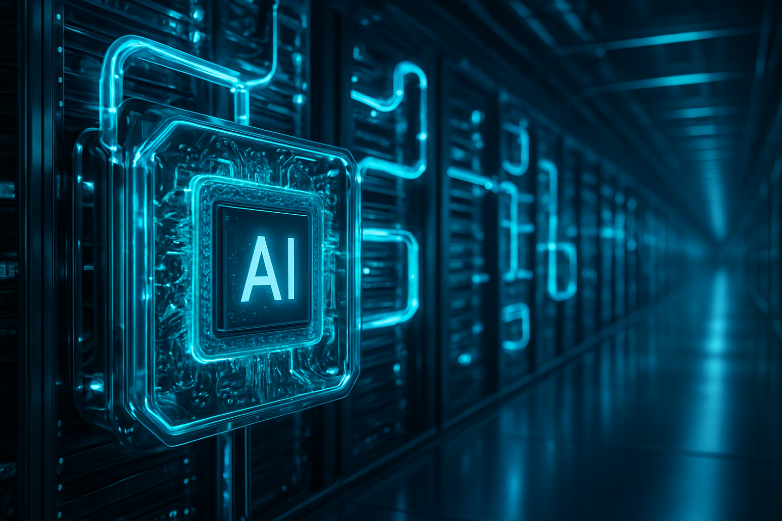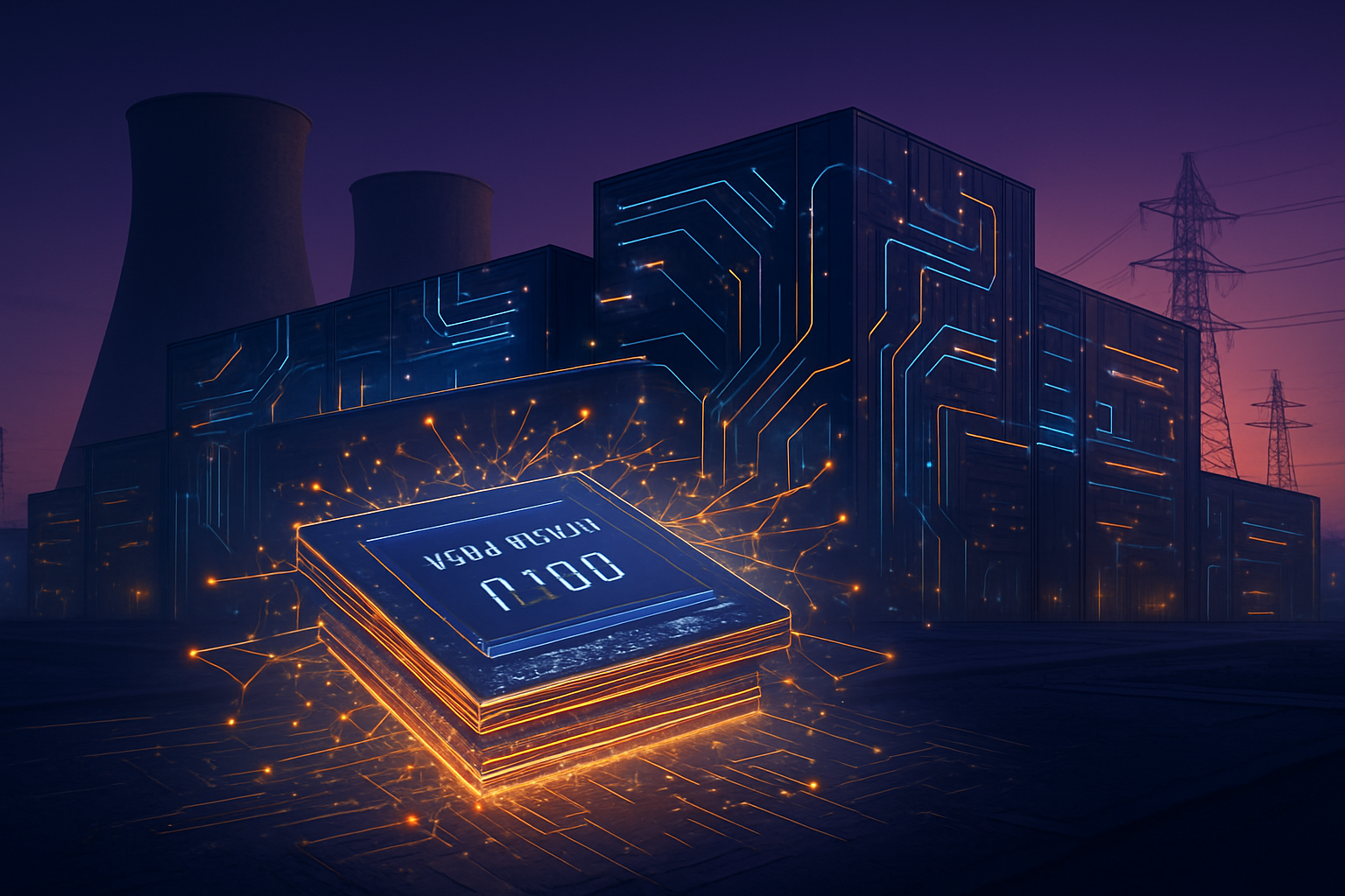
In a move that has fundamentally rewritten the economics of the silicon age, Nvidia (NASDAQ: NVDA) and OpenAI have announced a historic $100 billion strategic partnership aimed at constructing the most ambitious artificial intelligence infrastructure in human history. The deal, formalized as the "Sovereign Compute Pact," earmarks a staggering $100 billion in progressive investment from Nvidia to OpenAI, specifically designed to fund the deployment of 10 gigawatts (GW) of compute capacity over the next five years. This unprecedented infusion of capital is not merely a financial transaction; it is a full-scale industrial mobilization to build the "AI factories" required to achieve artificial general intelligence (AGI).
The immediate significance of this announcement cannot be overstated. By committing to a 10GW power envelope—a capacity roughly equivalent to the output of ten large nuclear power plants—the two companies are signaling that the "scaling laws" of AI are far from exhausted. Central to this expansion is the debut of Nvidia’s Vera Rubin platform, a next-generation architecture that represents the successor to the Blackwell line. Industry analysts suggest that this partnership effectively creates a vertically integrated "super-entity" capable of controlling the entire stack of intelligence, from the raw energy and silicon to the most advanced neural architectures in existence.
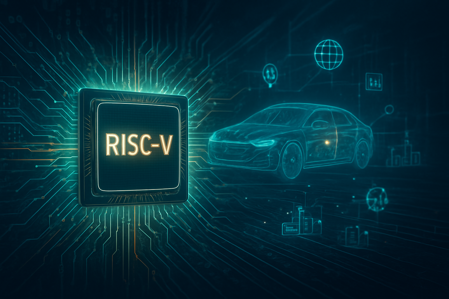
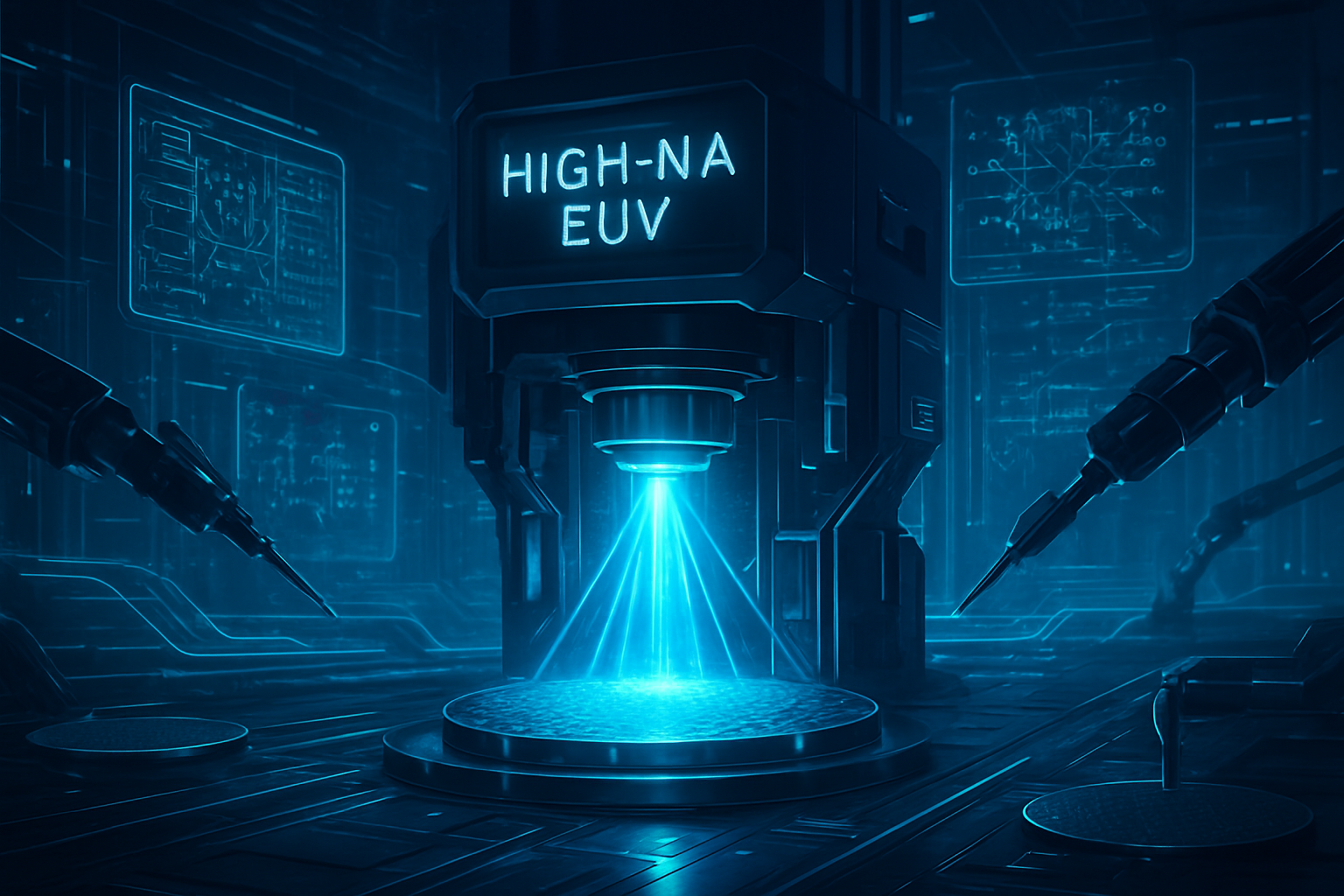
The Rubin Revolution: Inside the 10-Gigawatt Architecture
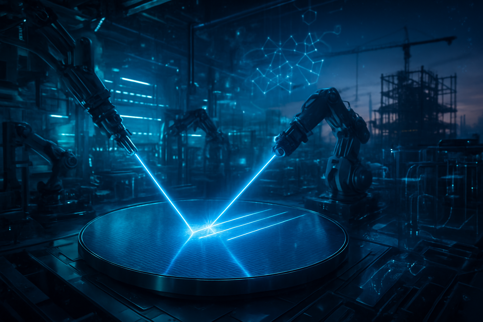
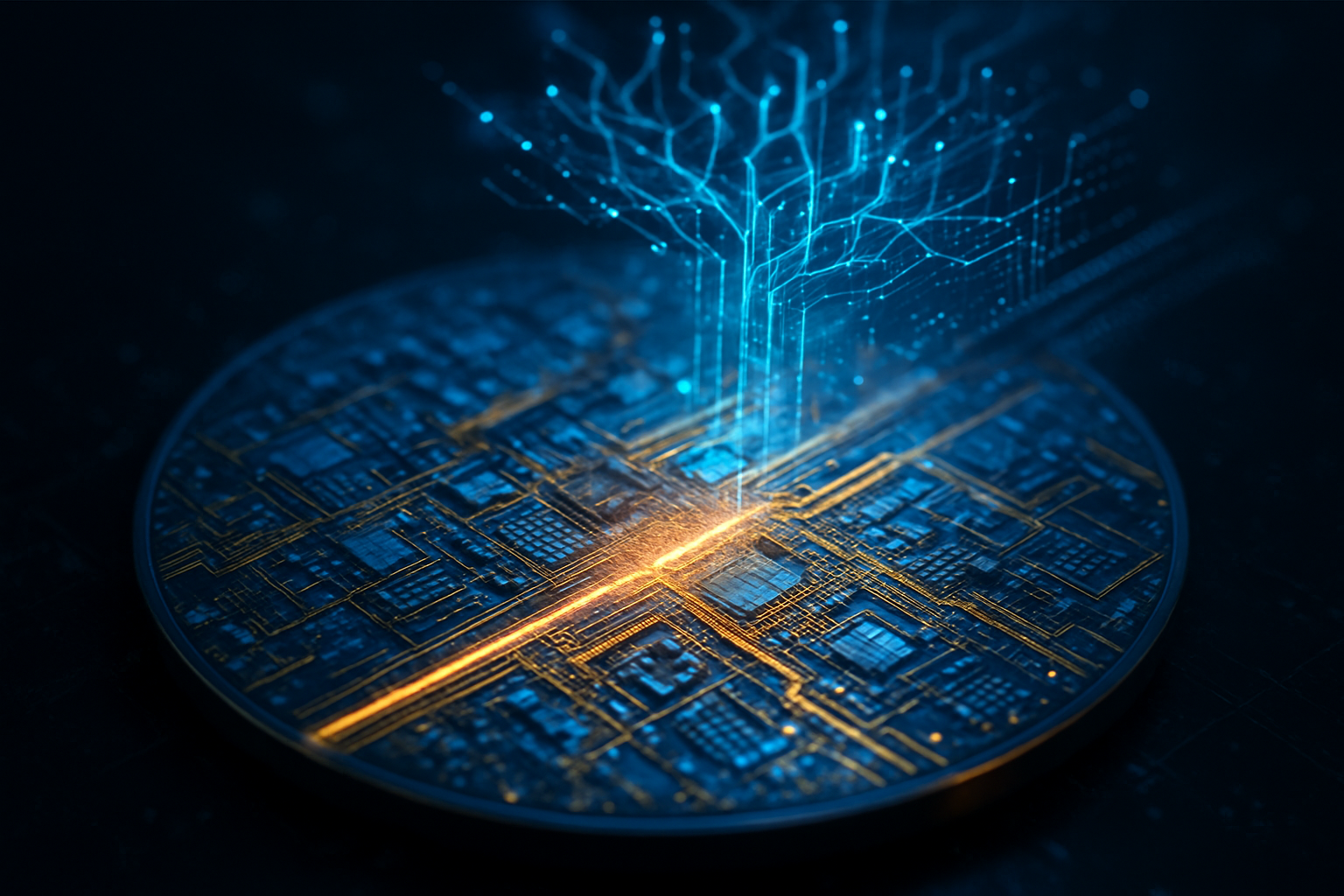
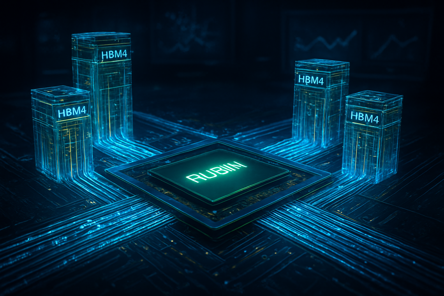
The technical backbone of this $100 billion expansion is the Vera Rubin platform, which Nvidia officially began shipping in late 2025. Unlike previous generations that focused on incremental gains in floating-point operations, the Rubin architecture is designed specifically for the "10GW era," where power efficiency and data movement are the primary bottlenecks. The core of the platform is the Rubin R100 GPU, manufactured on TSMC’s (NYSE: TSM) N3P (3-nanometer) process. The R100 features a "4-reticle" chiplet design, allowing it to pack significantly more transistors than its predecessor, Blackwell, while achieving a 25-30% reduction in power consumption per unit of compute.
One of the most radical departures from existing technology is the introduction of the Vera CPU, an 88-core custom ARM-based processor that replaces off-the-shelf designs. This allows for a "rack-as-a-computer" philosophy, where the CPU and GPU share a unified memory architecture supported by HBM4 (High Bandwidth Memory 4). With 288GB of HBM4 per GPU and a staggering 13 TB/s of memory bandwidth, the Vera Rubin platform is built to handle "million-token" context windows, enabling AI models to process entire libraries of data in a single pass. Furthermore, the infrastructure utilizes an 800V Direct Current (VDC) power delivery system and 100% liquid cooling, a necessity for managing the immense heat generated by 10GW of high-density compute.
Initial reactions from the AI research community have been a mix of awe and trepidation. Dr. Andrej Karpathy and other leading researchers have noted that this level of compute could finally solve the "reasoning gap" in current large language models (LLMs). By providing the hardware necessary for recursive self-improvement—where an AI can autonomously refine its own code—Nvidia and OpenAI are moving beyond simple pattern matching into the realm of synthetic logic. However, some hardware experts warn that the sheer complexity of the 800V DC infrastructure and the reliance on specialized liquid cooling systems could introduce new points of failure that the industry has never encountered at this scale.
A Seismic Shift in the Competitive Landscape
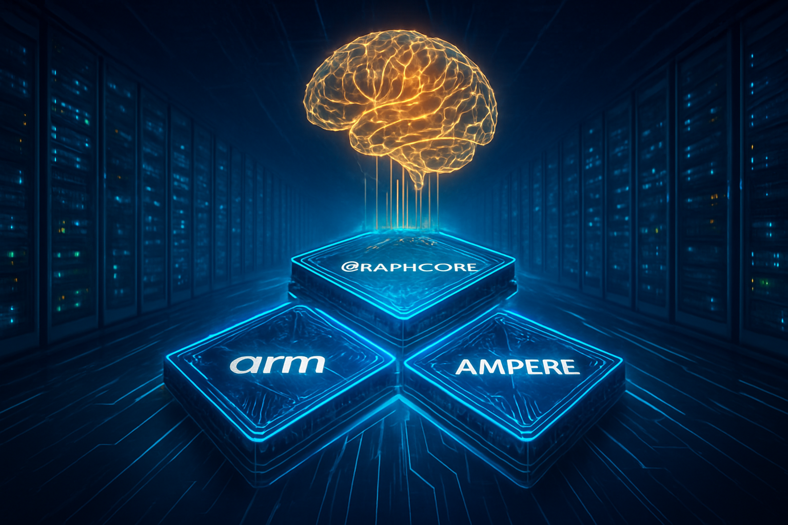
The Nvidia-OpenAI alliance has sent shockwaves through the tech industry, forcing rivals to form their own "counter-alliances." AMD (NASDAQ: AMD) has responded by deepening its ties with OpenAI through a 6GW "hedge" deal, where OpenAI will utilize AMD’s Instinct MI450 series in exchange for equity warrants. This move ensures that OpenAI is not entirely dependent on a single vendor, while simultaneously positioning AMD as the primary alternative for high-end AI silicon. Meanwhile, Alphabet (NASDAQ: GOOGL) has shifted its strategy, transforming its internal TPU (Tensor Processing Unit) program into a merchant vendor model. Google’s TPU v7 "Ironwood" systems are now being sold to external customers like Anthropic, creating a credible price-stabilizing force in a market otherwise dominated by Nvidia’s premium pricing.
For tech giants like Microsoft (NASDAQ: MSFT), which remains OpenAI’s largest cloud partner, the deal is a double-edged sword. While Microsoft benefits from the massive compute expansion via its Azure platform, the direct $100 billion link between Nvidia and OpenAI suggests a shifting power dynamic. The "Holy Trinity" of Microsoft, Nvidia, and OpenAI now controls the vast majority of the world’s high-end AI resources, creating a formidable barrier to entry for startups. Market analysts suggest that this consolidation may lead to a "compute-rich" vs. "compute-poor" divide, where only a handful of labs have the resources to train the next generation of frontier models.
The strategic advantage for Nvidia is clear: by becoming a major investor in its largest customer, it secures a guaranteed market for its most expensive chips for the next decade. This "circular economy" of AI—where Nvidia provides the chips, OpenAI provides the intelligence, and both share in the resulting trillions of dollars in value—is unprecedented in the history of the semiconductor industry. However, this has not gone unnoticed by regulators. The Department of Justice and the FTC have already begun preliminary probes into whether this partnership constitutes "exclusionary conduct," specifically regarding how Nvidia’s CUDA software and InfiniBand networking lock customers into a closed ecosystem.
The Energy Crisis and the Path to Superintelligence
The wider significance of a 10-gigawatt AI project extends far beyond the data center. The sheer energy requirement has forced a reckoning with the global power grid. To meet the 10GW target, OpenAI and Nvidia are pursuing a "nuclear-first" strategy, which includes partnering with developers of Small Modular Reactors (SMRs) and even participating in the restart of decommissioned nuclear sites like Three Mile Island. This move toward energy independence highlights a broader trend: AI companies are no longer just software firms; they are becoming heavy industrial players, rivaling the energy consumption of entire nations.
This massive scale-up is widely viewed as the "fuel" necessary to overcome the current plateaus in AI development. In the broader AI landscape, the move from "megawatt" to "gigawatt" compute marks the transition from LLMs to "Superintelligence." Comparisons are already being made to the Manhattan Project or the Apollo program, with the 10GW milestone representing the "escape velocity" needed for AI to begin autonomously conducting scientific research. However, environmental groups have raised significant concerns, noting that while the deal targets "clean" energy, the immediate demand for power could delay the retirement of fossil fuel plants, potentially offsetting the climate benefits of AI-driven efficiencies.
Regulatory and ethical concerns are also mounting. As the path to AGI becomes a matter of raw compute power, the question of "who controls the switch" becomes paramount. The concentration of 10GW of intelligence in the hands of a single alliance raises existential questions about global security and economic stability. If OpenAI achieves a "hard takeoff"—a scenario where the AI improves itself so rapidly that human oversight becomes impossible—the Nvidia-OpenAI infrastructure will be the engine that drives it.
The Road to GPT-6 and Beyond
Looking ahead, the near-term focus will be the release of GPT-6, expected in late 2026 or early 2027. Unlike its predecessors, GPT-6 is predicted to be the first truly "agentic" model, capable of executing complex, multi-step tasks across the physical and digital worlds. With the Vera Rubin platform’s massive memory bandwidth, these models will likely possess "permanent memory," allowing them to learn and adapt to individual users over years of interaction. Experts also predict the rise of "World Models," AI systems that don't just predict text but simulate physical reality, enabling breakthroughs in materials science, drug discovery, and robotics.
The challenges remaining are largely logistical. Building 10GW of capacity requires a global supply chain for high-voltage transformers, specialized cooling hardware, and, most importantly, a steady supply of HBM4 memory. Any disruption in the Taiwan Strait or a slowdown in TSMC’s 3nm yields could delay the project by years. Furthermore, as AI models grow more powerful, the "alignment problem"—ensuring the AI’s goals remain consistent with human values—becomes an engineering challenge of the same magnitude as the hardware itself.
A New Era of Industrial Intelligence
The $100 billion investment by Nvidia into OpenAI marks the end of the "experimental" phase of artificial intelligence and the beginning of the "industrial" era. It is a declaration that the future of the global economy will be built on a foundation of 10-gigawatt compute factories. The key takeaway is that the bottleneck for AI is no longer just algorithms, but the physical constraints of energy, silicon, and capital. By solving all three simultaneously, Nvidia and OpenAI have positioned themselves as the architects of the next century.
In the coming months, the industry will be watching closely for the first "gigawatt-scale" clusters to come online in late 2026. The success of the Vera Rubin platform will be the ultimate litmus test for whether the current AI boom can be sustained. As the "Sovereign Compute Pact" moves from announcement to implementation, the world is entering an era where intelligence is no longer a scarce human commodity, but a utility—as available and as powerful as the electricity that fuels it.
This content is intended for informational purposes only and represents analysis of current AI developments.
TokenRing AI delivers enterprise-grade solutions for multi-agent AI workflow orchestration, AI-powered development tools, and seamless remote collaboration platforms.
For more information, visit https://www.tokenring.ai/.