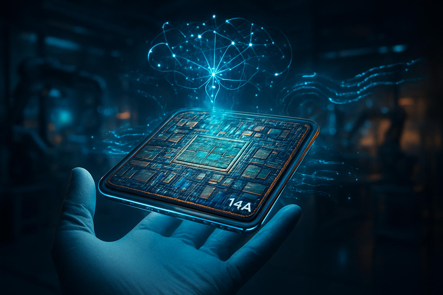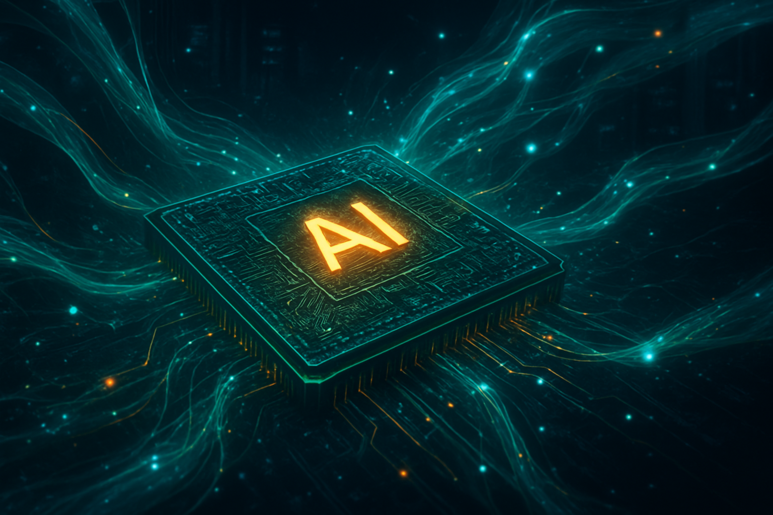
In a move that has sent shockwaves through Silicon Valley and the global semiconductor industry, NVIDIA (NASDAQ: NVDA) has finalized a blockbuster $20 billion agreement to license the intellectual property of AI chip innovator Groq and transition the vast majority of its engineering talent into the NVIDIA fold. The deal, structured as a strategic "license-and-acquihire," represents the largest single investment in NVIDIA’s history and marks a decisive pivot toward securing total dominance in the rapidly accelerating AI inference market.
The centerpiece of the agreement is the integration of Groq’s ultra-low-latency Language Processing Unit (LPU) technology and the appointment of Groq founder and Tensor Processing Unit (TPU) inventor Jonathan Ross to a senior leadership role within NVIDIA. By absorbing the team and technology that many analysts considered the most credible threat to its hardware hegemony, NVIDIA is effectively skipping years of research and development. This strategic strike not only neutralizes a potent rival but also positions NVIDIA to own the "real-time" AI era, where speed and efficiency in running models are becoming as critical as the power used to train them.
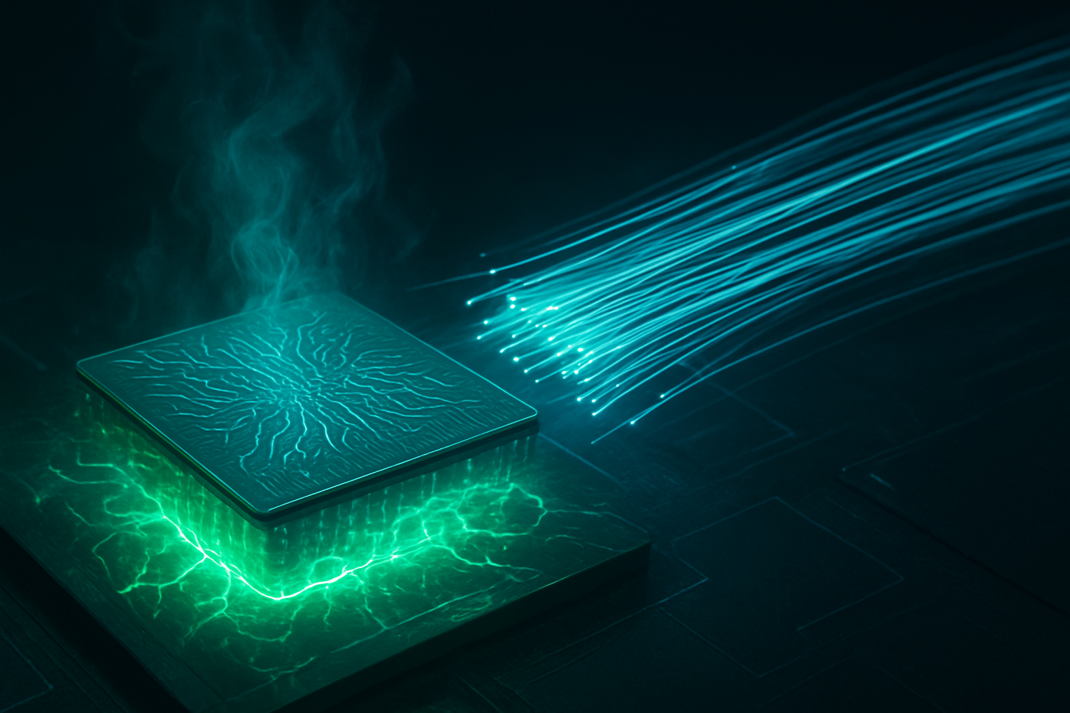
The LPU Advantage: Redefining AI Performance
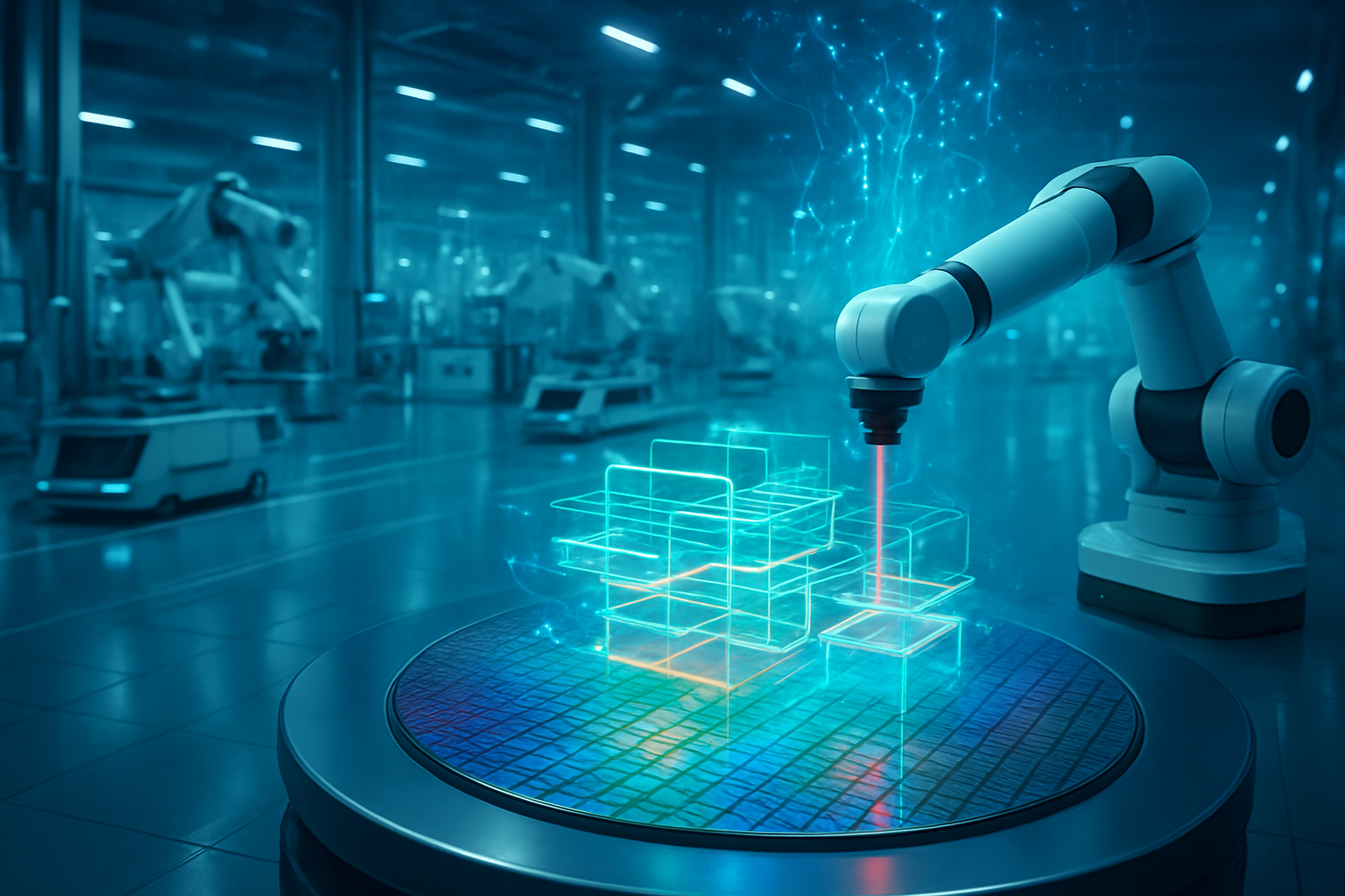
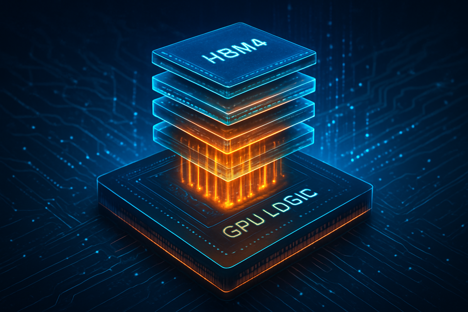
At the heart of this deal is Groq’s revolutionary LPU architecture, which differs fundamentally from the traditional Graphics Processing Units (GPUs) that have powered the AI boom to date. While GPUs are masters of parallel processing—handling thousands of small tasks simultaneously—they often struggle with the sequential nature of Large Language Models (LLMs), leading to "jitter" or variable latency. In contrast, the LPU utilizes a deterministic, single-core architecture. This design allows the system to know exactly where data is at any given nanosecond, resulting in predictable, sub-millisecond response times that are essential for fluid, human-like AI interactions.
Technically, the LPU’s secret weapon is its reliance on massive on-chip SRAM (Static Random-Access Memory) rather than the High Bandwidth Memory (HBM) used by NVIDIA’s current H100 and B200 chips. By keeping data directly on the processor, the LPU achieves a memory bandwidth of up to 80 terabytes per second—nearly ten times that of existing high-end GPUs. This architecture excels at "Batch Size 1" processing, meaning it can generate tokens for a single user instantly without needing to wait for other requests to bundle together. For the AI research community, this is a game-changer; it enables "instantaneous" reasoning in models like GPT-5 and Claude 4, which were previously bottlenecked by the physical limits of HBM data transfer.
Industry experts have reacted to the news with a mix of awe and caution. "NVIDIA just bought the fastest lane on the AI highway," noted one lead analyst at a major tech research firm. "By bringing Jonathan Ross—the man who essentially invented the modern AI chip at Google—into their ranks, NVIDIA isn't just buying hardware; they are buying the architectural blueprint for the next decade of computing."
Reshaping the Competitive Landscape
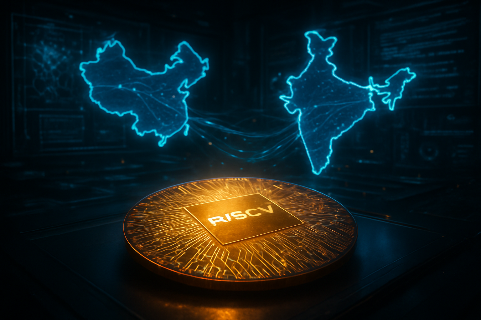
The strategic implications for the broader tech industry are profound. For years, major cloud providers and competitors like Alphabet Inc. (NASDAQ: GOOGL) and Advanced Micro Devices, Inc. (NASDAQ: AMD) have been racing to develop specialized inference ASICs (Application-Specific Integrated Circuits) to chip away at NVIDIA’s market share. Google’s TPU and Amazon’s Inferentia were designed specifically to offer a cheaper, faster alternative to NVIDIA’s general-purpose GPUs. By licensing Groq’s LPU technology, NVIDIA has effectively leapfrogged these custom solutions, offering a commercial product that matches or exceeds the performance of in-house hyperscaler silicon.
This deal creates a significant hurdle for other AI chip startups, such as Cerebras and Sambanova, who now face a competitor that possesses both the massive scale of NVIDIA and the specialized speed of Groq. Furthermore, the "license-and-acquihire" structure allows NVIDIA to avoid some of the regulatory scrutiny that would accompany a full acquisition. Because Groq will continue to exist as an independent entity operating its "GroqCloud" service, NVIDIA can argue it is fostering an ecosystem rather than absorbing it, even as it integrates Groq’s core innovations into its own future product lines.
For major AI labs like OpenAI and Anthropic, the benefit is immediate. Access to LPU-integrated NVIDIA hardware means they can deploy "agentic" AI—autonomous systems that can think, plan, and react in real-time—at a fraction of the current latency and power cost. This move solidifies NVIDIA’s position as the indispensable backbone of the AI economy, moving them from being the "trainers" of AI to the "engine" that runs it every second of the day.
From Training to Inference: The Great AI Shift
The $20 billion price tag reflects a broader trend in the AI landscape: the shift from the "Training Era" to the "Inference Era." While the last three years were defined by the massive clusters of GPUs needed to build models, the next decade will be defined by the trillions of queries those models must answer. Analysts predict that by 2030, the market for AI inference will be ten times larger than the market for training. NVIDIA’s move is a preemptive strike to ensure that as the industry evolves, its revenue doesn't peak with the completion of the world's largest data centers.
This acquisition draws parallels to NVIDIA’s 2020 purchase of Mellanox, which gave the company control over the high-speed networking (InfiniBand) necessary for massive GPU clusters. Just as Mellanox allowed NVIDIA to dominate training at scale, Groq’s technology will allow them to dominate inference at speed. However, this milestone is perhaps even more significant because it addresses the growing concern over AI's energy consumption. The LPU architecture is significantly more power-efficient for inference tasks than traditional GPUs, providing a path toward sustainable AI scaling as global power grids face increasing pressure.
Despite the excitement, the deal is not without its critics. Some in the open-source community express concern that NVIDIA’s tightening grip on both training and inference hardware could lead to a "black box" ecosystem where the most efficient AI can only run on proprietary NVIDIA stacks. This concentration of power in a single company’s hands remains a focal point for regulators in the US and EU, who are increasingly wary of "killer acquisitions" in the semiconductor space.
The Road Ahead: Real-Time Agents and "Vera Rubin"
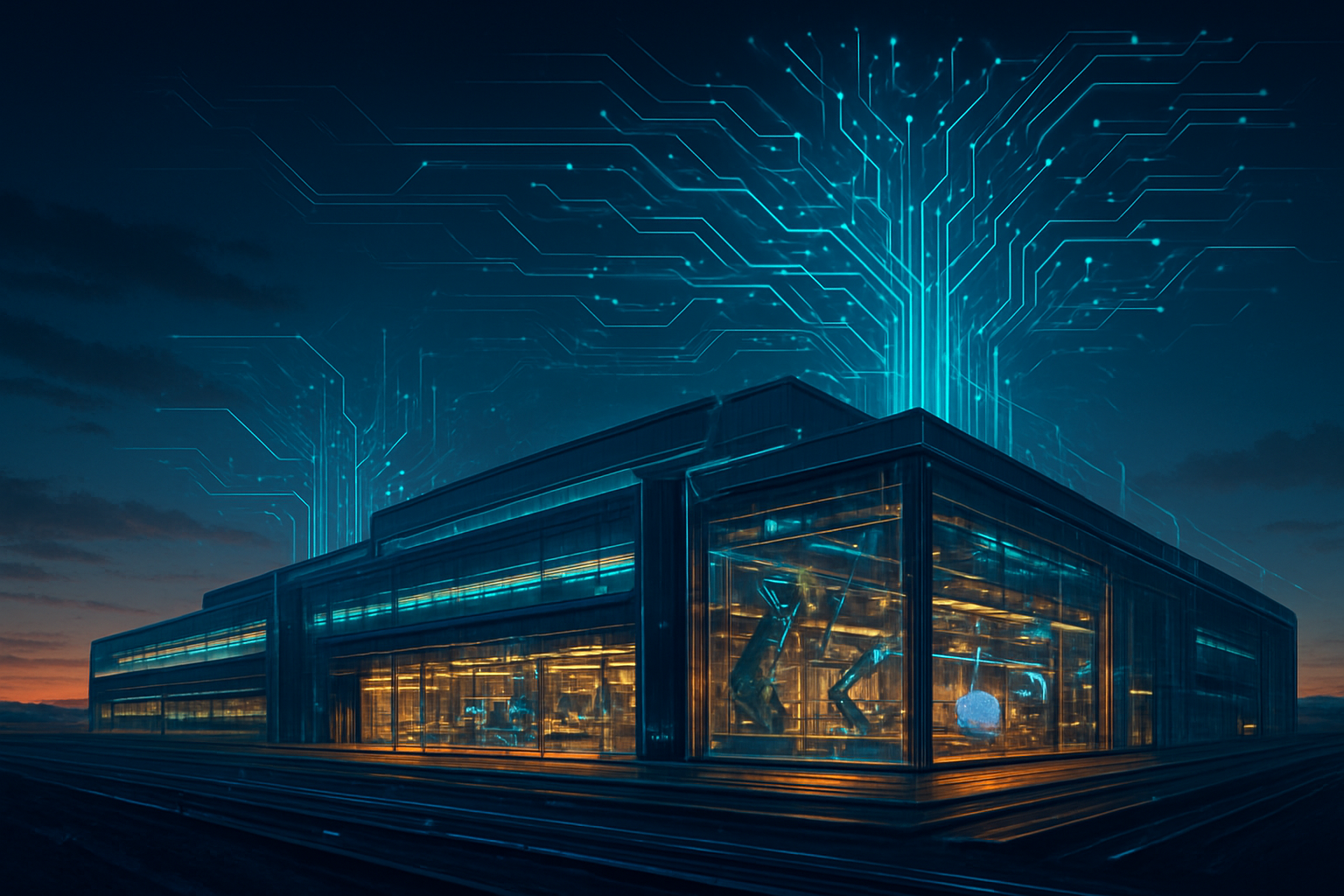
Looking toward the near-term future, the first fruits of this deal are expected to appear in NVIDIA’s 2026 hardware roadmap, specifically the rumored "Vera Rubin" architecture. Industry insiders suggest that NVIDIA will integrate LPU-derived "inference blocks" directly onto its next-generation dies, creating a hybrid chip capable of switching between heavy-lift training and ultra-fast inference seamlessly. This would allow a single server rack to handle the entire lifecycle of an AI model with unprecedented efficiency.
The most transformative applications will likely be in the realm of real-time AI agents. With the latency barriers removed, we can expect to see the rise of voice assistants that have zero "thinking" delay, real-time language translation that feels natural, and autonomous systems in robotics and manufacturing that can process visual data and make decisions in microseconds. The challenge for NVIDIA will be the complex task of merging Groq’s software-defined hardware approach with its own CUDA software stack, a feat of engineering that Jonathan Ross is uniquely qualified to lead.
Experts predict that the coming months will see a flurry of activity as NVIDIA's partners, including Microsoft Corp. (NASDAQ: MSFT) and Meta, scramble to secure early access to the first LPU-enhanced systems. The "race to zero latency" has officially begun, and with this $20 billion move, NVIDIA has claimed the pole position.
A New Chapter in the AI Revolution
NVIDIA’s licensing of Groq’s IP and the absorption of its engineering core represents a watershed moment in the history of computing. It is a clear signal that the "GPU-only" era of AI is evolving into a more specialized, diverse hardware landscape. By successfully identifying and integrating the most advanced inference technology on the market, NVIDIA has once again demonstrated the strategic agility that has made it one of the most valuable companies in the world.
The key takeaway for the industry is that the battle for AI supremacy has moved beyond who can build the largest model to who can deliver that model’s intelligence the fastest. As we look toward 2026, the integration of Groq’s deterministic architecture into the NVIDIA ecosystem will likely be remembered as the move that made real-time, ubiquitous AI a reality.
In the coming weeks, all eyes will be on the first joint technical briefings from NVIDIA and the former Groq team. As the dust settles on this $20 billion deal, the message to the rest of the industry is clear: NVIDIA is no longer just a chip company; it is the architect of the real-time intelligent world.
This content is intended for informational purposes only and represents analysis of current AI developments.
TokenRing AI delivers enterprise-grade solutions for multi-agent AI workflow orchestration, AI-powered development tools, and seamless remote collaboration platforms.
For more information, visit https://www.tokenring.ai/.