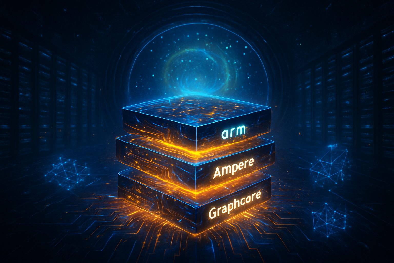
As of late December 2025, the semiconductor industry has reached a historic inflection point that many analysts once thought impossible. Intel (NASDAQ:INTC) has officially successfully executed its "five nodes in four years" roadmap, culminating in the mid-2025 volume production of its 18A (1.8nm) process node. This achievement has effectively allowed the American chipmaker to leapfrog the industry’s traditional leader, Taiwan Semiconductor Manufacturing Company (NYSE:TSM), in the race to deploy the next generation of transistor architecture. With Intel’s "Panther Lake" processors already shipping to hardware partners for a January 2026 retail launch, the battle for silicon supremacy has moved from the laboratory to the high-volume factory floor.
The significance of this moment cannot be overstated. For the first time in nearly a decade, the "process lead"—the metric by which the world’s most advanced chips are judged—is no longer a foregone conclusion in favor of TSMC. While TSMC has begun series production of its own N2 (2nm) node in late 2025, Intel’s early aggressive push with 18A has created a competitive vacuum. This shift is driving a massive realignment in the high-performance computing and AI sectors, as tech giants weigh the technical advantages of Intel’s new architecture against the legendary reliability and scale of the Taiwanese foundry.
Technical Frontiers: RibbonFET and the PowerVia Advantage
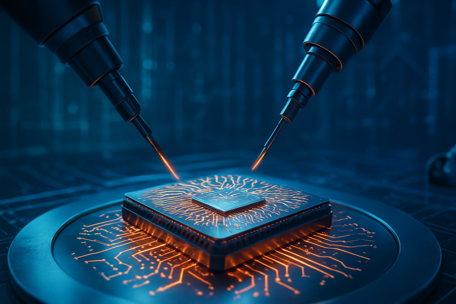
The transition to the 2nm class represents the most radical architectural change in semiconductors since the introduction of FinFET over a decade ago. Both Intel and TSMC have moved to Gate-All-Around (GAA) transistors—which Intel calls RibbonFET and TSMC calls Nanosheet GAA—to overcome the physical limitations of current designs. However, the technical differentiator that has put Intel in the spotlight is "PowerVia," the company's proprietary implementation of Backside Power Delivery (BSPDN). By moving power routing to the back of the wafer, Intel has decoupled power and signal wires, drastically reducing electrical interference and "voltage droop." This allows 18A chips to achieve higher clock speeds at lower voltages, a critical requirement for the energy-hungry AI workloads of 2026.
In contrast, TSMC’s initial N2 node, while utilizing a highly refined Nanosheet GAA structure, has opted for a more conservative approach by maintaining traditional frontside power delivery. While this strategy has allowed TSMC to maintain slightly higher initial yields—reported at approximately 65–70% compared to Intel’s 55–65%—it leaves a performance gap that Intel is eager to exploit. TSMC’s version of backside power, the "Super Power Rail," is not scheduled to debut until the N2P and A16 (1.6nm) nodes arrive late in 2026 and throughout 2027. This technical window has given Intel a temporary but potent "performance-per-watt" lead that is reflected in the early benchmarks of its Panther Lake and Clearwater Forest architectures.
Initial reactions from the semiconductor research community have been cautiously optimistic. Experts note that while Intel’s 18A density (roughly 238 million transistors per square millimeter) still trails TSMC’s N2 density (over 310 MTr/mm²), the efficiency gains from PowerVia may matter more for real-world AI performance than raw density alone. The industry is closely watching the "Panther Lake" (Core Ultra Series 3) launch, as it will be the first high-volume consumer product to prove whether Intel can maintain these technical gains without the manufacturing "stumbles" that plagued its 10nm and 7nm efforts years ago.
The Foundry War: Client Loyalty and Strategic Shifts
The business implications of this race are reshaping the landscape for AI companies and tech giants. Intel Foundry has already secured high-profile commitments from Microsoft (NASDAQ:MSFT) for its Maia 2 AI accelerators and Amazon (NASDAQ:AMZN) for custom Xeon 6 fabric silicon. These partnerships are a massive vote of confidence in Intel’s 18A node and signal a desire among US-based hyperscalers to diversify their supply chains away from a single-source reliance on Taiwan. For Intel, these "anchor" customers provide the volume necessary to refine 18A yields and fund the even more ambitious 14A node slated for 2027.
Meanwhile, TSMC remains the dominant force by sheer volume and ecosystem maturity. Apple (NASDAQ:AAPL) has reportedly secured nearly 50% of TSMC’s initial N2 capacity for its upcoming A20 and M5 chips, ensuring that the next generation of iPhones and Macs remains at the bleeding edge. Similarly, Nvidia (NASDAQ:NVDA) is sticking with TSMC for its "Rubin" GPU successor, citing the foundry’s superior CoWoS packaging capabilities as a primary reason. However, the fact that Nvidia has reportedly kept a "placeholder" for testing Intel’s 18A yields suggests that even the AI kingpin is keeping its options open should Intel’s performance lead prove durable through 2026.
This competition is disrupting the "wait-and-see" approach previously taken by many fabless startups. With Intel 18A offering a faster path to backside power delivery, some AI hardware startups are pivoting their designs to Intel’s PDKs (Process Design Kits) to gain a first-mover advantage in efficiency. The market positioning is clear: Intel is marketing itself as the "performance leader" for those who need the latest architectural breakthroughs now, while TSMC positions itself as the "reliable scale leader" for the world’s largest consumer electronics brands.
Geopolitics and the End of the FinFET Era
The broader significance of the 2nm race extends far beyond chip benchmarks; it is a central pillar of global technological sovereignty. Intel’s success with 18A is a major win for the U.S. CHIPS Act, as the node is being manufactured at scale in Fab 52 in Arizona. This represents a tangible shift in the geographic concentration of advanced logic manufacturing. As the world moves into the post-FinFET era, the ability to manufacture GAA transistors at scale has become the new baseline for being a "tier-one" tech superpower.
This milestone also echoes previous industry shifts, such as the move from planar transistors to FinFET in 2011. Just as that transition allowed for the smartphone revolution, the move to 2nm and 1.8nm is expected to fuel the next decade of "Edge AI." By providing the thermal headroom needed to run large language models (LLMs) locally on laptops and mobile devices, these new nodes are the silent engines behind the AI software boom. The potential concern remains the sheer cost of these chips; as wafer prices for 2nm are expected to exceed $30,000, the "digital divide" between companies that can afford the latest silicon and those that cannot may widen.
Future Outlook: The Road to 14A and A16
Looking ahead to 2026, the industry will focus on the ramp-up of consumer availability. While Intel’s Panther Lake will dominate the conversation in early 2026, the second half of the year will see the debut of TSMC’s N2 in the iPhone 18, likely reclaiming the crown for mobile efficiency. Furthermore, the arrival of High-NA EUV (Extreme Ultraviolet) lithography machines from ASML (NASDAQ:ASML) will become the next battleground. Intel has already taken delivery of the first High-NA units to prepare for its 14A node, while TSMC has indicated it may wait until 2026 or 2027 to integrate the expensive new tools into its A16 process.
Experts predict that the "lead" will likely oscillate between the two giants every 12 to 18 months. The next major hurdle will be the integration of "optical interconnects" and even more advanced 3D packaging, as the industry realizes that the transistor itself is no longer the only bottleneck. The success of Intel’s Clearwater Forest in mid-2026 will be the ultimate test of whether 18A can handle the grueling demands of the data center at scale, potentially paving the way for a permanent "dual-foundry" world where Intel and TSMC share the top spot.
A New Era of Silicon Competition
The 2nm manufacturing race of 2025-2026 marks the end of Intel’s period of "catch-up" and the beginning of a genuine two-way fight for the future of computing. By hitting volume production with 18A in mid-2025 and beating TSMC to the implementation of backside power delivery, Intel has proven that its turnaround strategy under Pat Gelsinger was more than just corporate rhetoric. However, TSMC’s massive capacity and deep-rooted relationships with Apple and Nvidia mean that the Taiwanese giant is far from losing its throne.
As we move into early 2026, the key takeaways are clear: the era of FinFET is over, "PowerVia" is the new technical gold standard, and the geographic map of chip manufacturing is successfully diversifying. For consumers, this means more powerful "AI PCs" and smartphones are just weeks away from store shelves. For the industry, it means the most competitive and innovative period in semiconductor history has only just begun. Watch for the CES 2026 announcements in January, as they will provide the first retail evidence of who truly won the 2nm punch.
This content is intended for informational purposes only and represents analysis of current AI developments.
TokenRing AI delivers enterprise-grade solutions for multi-agent AI workflow orchestration, AI-powered development tools, and seamless remote collaboration platforms.
For more information, visit https://www.tokenring.ai/.