As 2025 draws to a close, the global automotive industry is undergoing a foundational shift in its power architecture, moving away from traditional silicon toward wide-bandgap (WBG) materials like Silicon Carbide (SiC) and Gallium Nitride (GaN). At the heart of this transition is ON Semiconductor (Nasdaq: ON), which has spent the final quarter of 2025 cementing its status as the linchpin of the electric vehicle (EV) supply chain. With the recent announcement of a massive $6 billion share buyback program and the finalization of a $2 billion expansion in the Czech Republic, onsemi is signaling that the era of "range anxiety" is being replaced by an era of high-efficiency, AI-optimized power delivery.
The significance of this moment cannot be overstated. As of December 29, 2025, the industry has reached a tipping point where 800-volt EV architectures—which allow for ultra-fast charging and significantly lighter wiring—have moved from niche luxury features to the standard for mid-market vehicles. This shift is driven almost entirely by the superior thermal and electrical properties of SiC and GaN. By enabling power inverters to operate at higher temperatures and frequencies with minimal energy loss, these materials are effectively adding up to 7% more range to EVs without increasing battery size, a breakthrough that is reshaping the economics of sustainable transport.
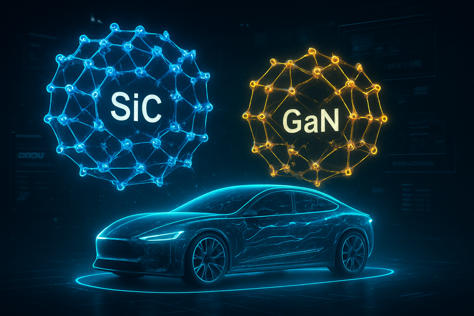
Technical Breakthroughs: EliteSiC M3e and the Rise of Vertical GaN
The technical narrative of 2025 has been dominated by onsemi’s mass production of its EliteSiC M3e MOSFET technology. Unlike previous generations of planar SiC devices, the M3e architecture has successfully reduced conduction losses by a staggering 30%, a feat that was previously thought to require a more complex transition to trench-based designs. This efficiency gain is critical for the latest generation of traction inverters, which convert DC battery power into the AC power that drives the vehicle’s motors. Industry experts have noted that the M3e’s ability to handle higher power densities has allowed OEMs to shrink the footprint of the power electronics bay by nearly 20%, providing more cabin space and improving vehicle aerodynamics.
Parallel to the SiC advancement is the emergence of Vertical GaN technology, which onsemi unveiled in late 2025. While traditional GaN has been limited to lower-power applications like on-board chargers and DC-DC converters, Vertical GaN aims to bring GaN’s extreme switching speeds to the high-power traction inverter. This development is particularly relevant for the AI-driven mobility sector; as EVs become increasingly autonomous, the demand for high-speed data processing and real-time power modulation grows. Vertical GaN allows for the kind of rapid-response power switching required by AI-managed drivetrains, which can adjust torque and energy consumption in millisecond intervals based on road conditions and sensor data.
The transition from 6-inch to 8-inch (200mm) SiC wafers has also reached a critical milestone this month. By moving to larger wafers, onsemi and its peers are achieving significant economies of scale, effectively lowering the cost-per-die. This manufacturing evolution is what has finally allowed SiC to compete on a cost-basis with traditional silicon in the $35,000 to $45,000 EV price bracket. Initial reactions from the research community suggest that the 8-inch transition is the "Moore’s Law moment" for power electronics, paving the way for a 2026 where high-efficiency semiconductors are no longer a premium bottleneck but a commodity staple.
Market Dominance and Strategic Financial Maneuvers
Financially, onsemi is ending 2025 in a position of unprecedented strength. The company’s board recently authorized a new $6 billion share repurchase program set to begin on January 1, 2026. This follows a year in which onsemi returned nearly 100% of its free cash flow to shareholders, a move that has bolstered investor confidence despite the capital-intensive nature of semiconductor fabrication. By committing to return roughly one-third of its market capitalization over the next three years, onsemi is positioning itself as the "value play" in a high-growth sector, distinguishing itself from more volatile competitors like Wolfspeed (NYSE: WOLF).
The competitive landscape has also been reshaped by onsemi’s $2 billion investment in Rožnov, Czech Republic. With the European Commission recently approving €450 million in state aid under the European Chips Act, this facility is set to become Europe’s first vertically integrated SiC manufacturing hub. This move provides a strategic advantage over STMicroelectronics (NYSE: STM) and Infineon Technologies (OTC: IFNNY), as it secures a localized, resilient supply chain for European giants like Volkswagen and BMW. Furthermore, onsemi’s late-2025 partnership with GlobalFoundries (Nasdaq: GFS) to co-develop 650V GaN products indicates a multi-pronged approach to dominating both the high-power and mid-power segments of the market.
Market analysts point out that onsemi’s aggressive expansion in China has also paid dividends. In 2025, the company’s SiC revenue in the Chinese market doubled, driven by deep integration with domestic OEMs like Geely. While other Western tech firms have struggled with geopolitical headwinds, onsemi’s "brownfield" strategy—upgrading existing facilities rather than building entirely new ones—has allowed it to scale faster and more efficiently than its rivals. This strategic positioning has made onsemi the primary beneficiary of the global shift toward 800V platforms, leaving competitors scrambling to catch up with its production yields.
The Wider Significance: AI, Decarbonization, and the New Infrastructure
The growth of SiC and GaN is more than just an automotive story; it is a fundamental component of the broader AI and green energy landscape. In late 2025, we are seeing a convergence between EV power electronics and AI data center infrastructure. The same Vertical GaN technology that enables faster EV charging is now being deployed in the power supply units (PSUs) of AI server racks. As AI models grow in complexity, the energy required to train them has skyrocketed, making power efficiency a top-tier operational priority. Wide-bandgap semiconductors are the only viable solution for reducing the massive heat signatures and energy waste associated with the next generation of AI chips.
This development fits into a broader trend of "Electrification 2.0," where the focus has shifted from merely building batteries to optimizing how every milliwatt of power is used. The integration of AI-optimized power management systems—software that uses machine learning to predict power demand and adjust semiconductor switching in real-time—is becoming a standard feature in both EVs and smart grids. By reducing energy loss during power conversion, onsemi’s hardware is effectively acting as a catalyst for global decarbonization efforts, making the transition to renewable energy more economically viable.
However, the rapid adoption of these materials is not without concerns. The industry remains heavily reliant on a few key geographic regions for raw materials, and the environmental impact of SiC crystal growth—a high-heat, energy-intensive process—is under increasing scrutiny. Comparisons are being drawn to the early days of the microprocessor boom; while the benefits are immense, the sustainability of the supply chain will be the defining challenge of the late 2020s. Experts warn that without continued innovation in recycling and circular manufacturing, the "green" revolution could face its own resource constraints.
Looking Ahead: The 2026 Outlook and Beyond
As we look toward 2026, the industry is bracing for the full-scale implementation of the 8-inch wafer transition. This move is expected to further depress prices, potentially leading to a "price war" in the SiC space that could force consolidation among smaller players. We also expect to see the first commercial vehicles featuring GaN in the main traction inverter by late 2026, a milestone that would represent the final frontier for Gallium Nitride in the automotive sector.
Near-term developments will likely focus on "integrated power modules," where SiC MOSFETs are packaged directly with AI-driven controllers. This "smart power" approach will allow for even greater levels of efficiency and predictive maintenance, where a vehicle can diagnose a potential inverter failure before it occurs. Predictably, the next big challenge will be the integration of these semiconductors into the burgeoning "Vehicle-to-Grid" (V2G) infrastructure, where EVs act as mobile batteries to stabilize the power grid during peak demand.
Summary of the High-Voltage Shift
The events of late 2025 have solidified Silicon Carbide and Gallium Nitride as the "new oil" of the automotive and AI industries. ON Semiconductor’s strategic pivot toward vertical integration and aggressive capital returns has positioned it as the dominant leader in this space. By successfully scaling the EliteSiC M3e platform and securing a foothold in the European and Chinese markets, onsemi has turned the technical advantages of wide-bandgap materials into a formidable economic moat.
As we move into 2026, the focus will shift from proving the technology to perfecting the scale. The transition to 8-inch wafers and the rise of Vertical GaN represent the next chapter in a story that is as much about energy efficiency as it is about transportation. For investors and industry watchers alike, the coming months will be defined by how well these companies can manage their massive capacity expansions while navigating a complex geopolitical and environmental landscape. One thing is certain: the high-voltage revolution is no longer a future prospect—it is the present reality.
This content is intended for informational purposes only and represents analysis of current AI developments.
TokenRing AI delivers enterprise-grade solutions for multi-agent AI workflow orchestration, AI-powered development tools, and seamless remote collaboration platforms.
For more information, visit https://www.tokenring.ai/.