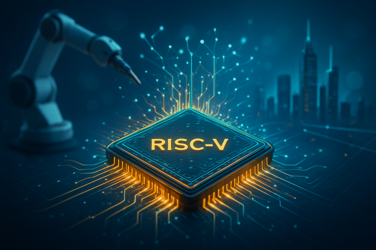
As of late 2025, the global semiconductor landscape has reached a definitive turning point. The rise of RISC-V, an open-standard instruction set architecture (ISA), has transitioned from a niche academic interest to a geopolitical necessity. Driven by the dual engines of China’s need to bypass Western trade restrictions and the European Union’s quest for "strategic autonomy," RISC-V has emerged as the third pillar of computing, challenging the long-standing duopoly of x86 and ARM.
This shift is not merely about cost-saving; it is a fundamental reconfiguration of how nations secure their digital futures. With the official finalization of the RVA23 profile and the deployment of high-performance AI accelerators, RISC-V is now the primary vehicle for "sovereign silicon." By Decemeber 2025, industry analysts confirm that RISC-V-based processors account for nearly 25% of the global market share in specialized AI and IoT sectors, signaling a permanent departure from the proprietary dominance of the past four decades.
The Technical Leap: RVA23 and the Era of High-Performance Open Silicon
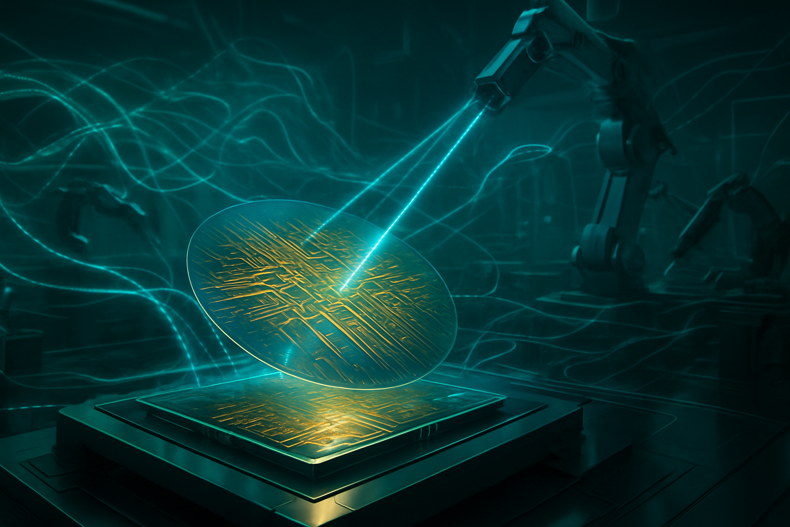
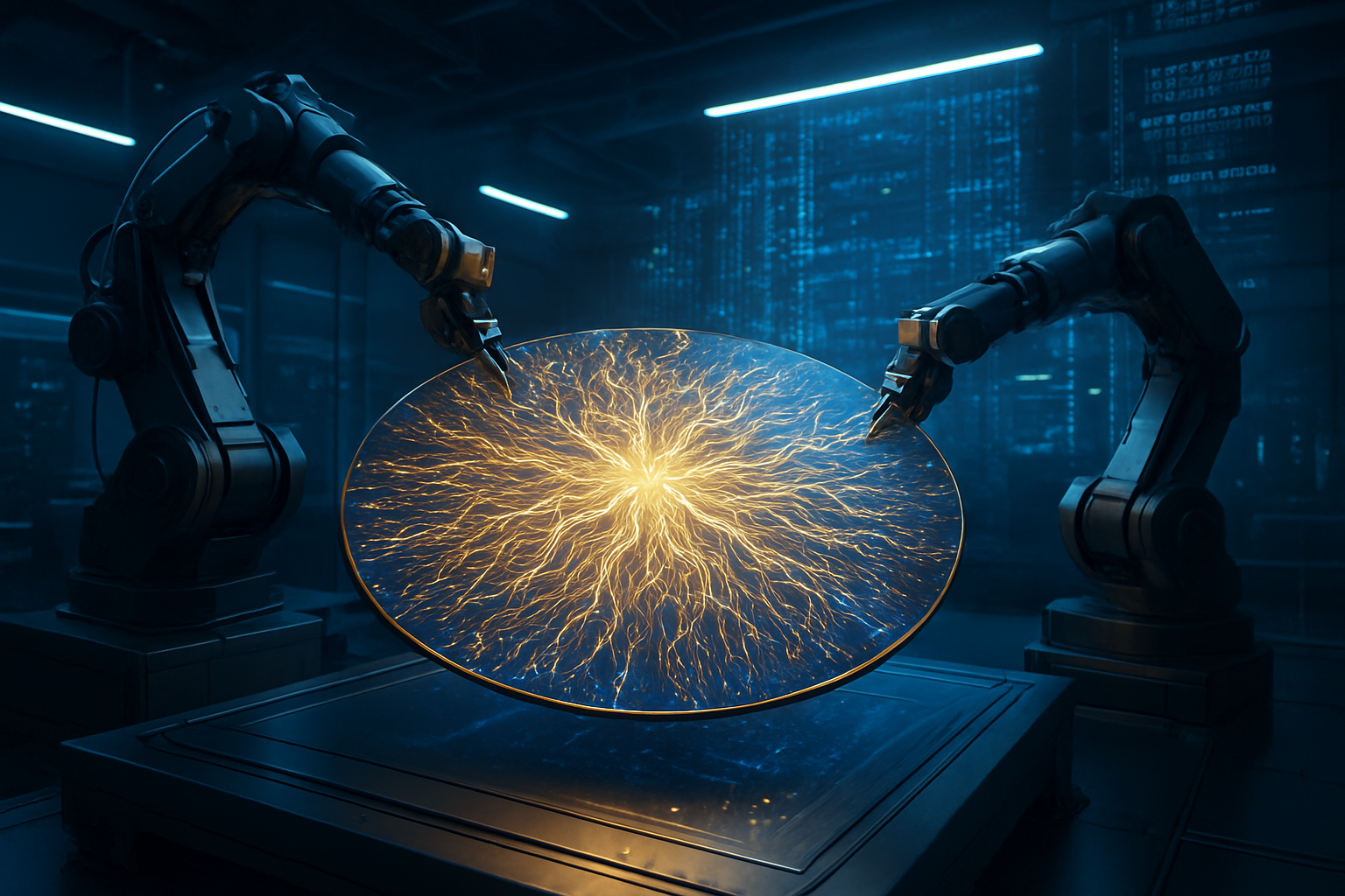
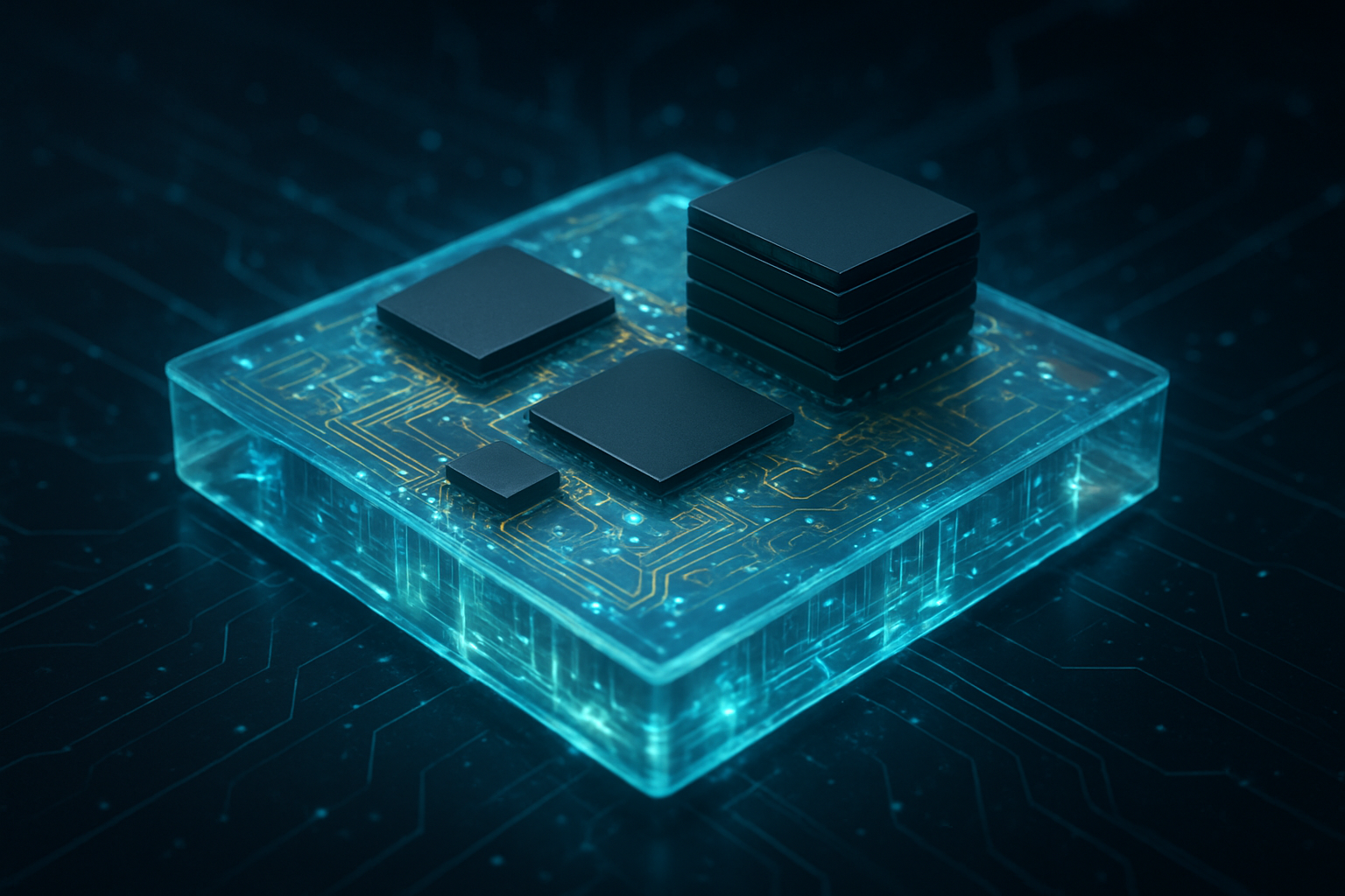
The technical maturity of RISC-V in late 2025 is anchored by the widespread adoption of the RVA23 profile. This standardization milestone has resolved the fragmentation issues that previously plagued the ecosystem, mandating critical features such as Hypervisor extensions, Bitmanip, and most importantly, Vector 1.0 (RVV). These capabilities allow RISC-V chips to handle the complex, math-intensive workloads required for modern generative AI and autonomous robotics. A standout example is the XuanTie C930, released by T-Head, the semiconductor arm of Alibaba Group Holding Limited (NYSE: BABA). The C930 is a server-grade 64-bit multi-core processor that integrates a specialized 8 TOPS Matrix engine, specifically designed to accelerate AI inference at the edge and in the data center.
Parallel to China's commercial success, the third generation of the "Kunminghu" architecture—developed by the Chinese Academy of Sciences—has pushed the boundaries of open-source performance. Clocking in at 3GHz and built on advanced process nodes, the Kunminghu Gen 3 rivals the performance of the Neoverse N2 from Arm Holdings plc (NASDAQ: ARM). This achievement proves that open-source hardware can compete at the highest levels of cloud computing. Meanwhile, in the West, Tenstorrent—led by legendary architect Jim Keller—has entered full production of its Ascalon core. By decoupling the CPU from proprietary licensing, Tenstorrent has enabled a modular "chiplet" approach that allows companies to mix and match AI accelerators with RISC-V management cores, a flexibility that traditional architectures struggle to match.
The European front has seen equally significant technical breakthroughs through the Digital Autonomy with RISC-V in Europe (DARE) project. Launched in early 2025, DARE has successfully produced the "Titania" AI Processing Unit (AIPU), which utilizes Digital In-Memory Computing (D-IMC) to achieve unprecedented energy efficiency in robotics. These advancements differ from previous approaches by removing the "black box" nature of proprietary ISAs. For the first time, researchers and sovereign states can audit every line of the instruction set, ensuring there are no hardware-level backdoors—a critical requirement for national security and critical infrastructure.
Market Disruption: The End of the Proprietary Duopoly?
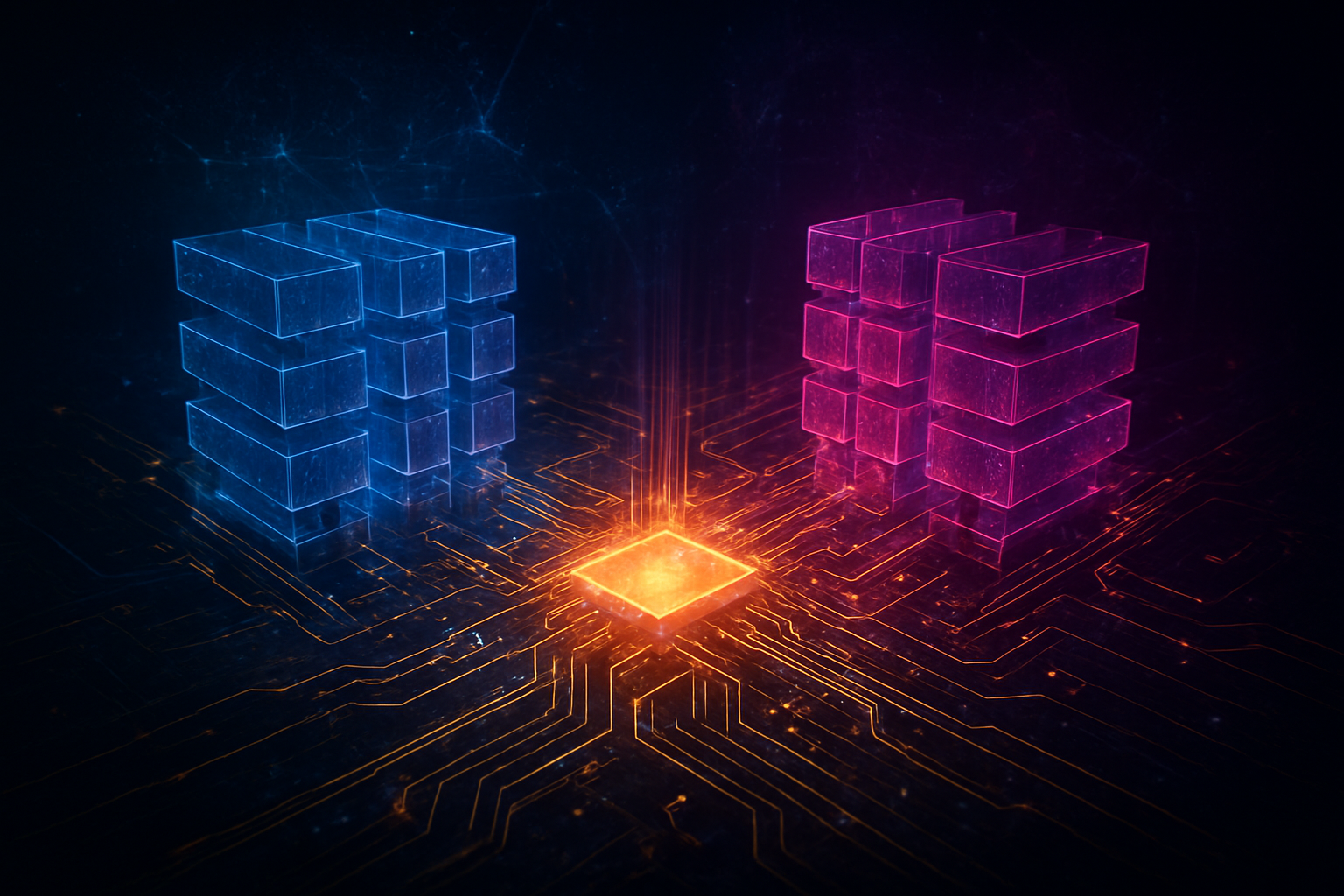
The acceleration of RISC-V is creating a seismic shift in the competitive dynamics of the semiconductor industry. Companies like Alibaba (NYSE: BABA) and various state-backed Chinese entities have effectively neutralized the impact of U.S. export controls by building a self-sustaining domestic ecosystem. China now accounts for nearly 50% of all global RISC-V shipments, a statistic that has forced a strategic pivot from established giants. While Intel Corporation (NASDAQ: INTC) and NVIDIA Corporation (NASDAQ: NVDA) continue to dominate the high-end GPU and server markets, the erosion of their "moats" in specialized AI accelerators and edge computing is becoming evident.
Major AI labs and tech startups are the primary beneficiaries of this shift. By utilizing RISC-V, startups can avoid the hefty licensing fees and restrictive "take-it-or-leave-it" designs associated with proprietary vendors. This has led to a surge in bespoke AI hardware tailored for specific tasks, such as humanoid robotics and real-time language translation. The strategic advantage has shifted toward "vertical integration," where a company can design a chip, the compiler, and the AI model in a single, unified pipeline. This level of customization was previously the exclusive domain of trillion-dollar tech titans; in 2025, it is becoming the standard for any well-funded AI startup.
However, the transition has not been without its casualties. The traditional "IP licensing" business model is under intense pressure. As RISC-V matures, the value proposition of paying for a standard ISA is diminishing. We are seeing a "race to the top" where proprietary providers must offer significantly more than just an ISA—such as superior interconnects, software stacks, or support—to justify their costs. The market positioning of ARM, in particular, is being squeezed between the high-performance dominance of x86 and the open-source flexibility of RISC-V, leading to a more fragmented but competitive global hardware market.
Geopolitical Significance: The Search for Strategic Autonomy
The rise of RISC-V is inextricably linked to the broader trend of "technological decoupling." For China, RISC-V is a defensive necessity—a way to ensure that its massive AI and robotics industries can continue to function even under the most stringent sanctions. The late 2025 policy framework finalized by eight Chinese government agencies treats RISC-V as a national priority, effectively mandating its use in government procurement and critical infrastructure. This is not just a commercial move; it is a survival strategy designed to insulate the Chinese economy from external geopolitical shocks.
In Europe, the motivation is slightly different but equally potent. The EU's push for "strategic autonomy" is driven by a desire to not be caught in the crossfire of the U.S.-China tech war. By investing in projects like the European Processor Initiative (EPI) and DARE, the EU is building a "third way" that relies on open standards rather than the goodwill of foreign corporations. This fits into a larger trend where data privacy, hardware security, and energy efficiency are viewed as sovereign rights. The successful deployment of Europe’s first Out-of-Order (OoO) RISC-V silicon in October 2025 marks a milestone in this journey, proving that the continent can design and manufacture its own high-performance logic.
The wider significance of this movement cannot be overstated. It mirrors the rise of Linux in the software world decades ago. Just as Linux broke the monopoly of proprietary operating systems and became the backbone of the internet, RISC-V is becoming the backbone of the "Internet of Intelligence." However, this shift also brings concerns regarding fragmentation. If China and the EU develop significantly different extensions for RISC-V, the dream of a truly global, open standard could splinter into regional "walled gardens." The industry is currently watching the RISE (RISC-V Software Ecosystem) project closely to see if it can maintain a unified software layer across these diverse hardware implementations.
Future Horizons: From Data Centers to Humanoid Robots
Looking ahead to 2026 and beyond, the focus of RISC-V development is shifting toward two high-growth areas: data center CPUs and embodied AI. Tenstorrent’s roadmap for its Callandor core, slated for 2027, aims to challenge the fastest proprietary CPUs in the world. If successful, this would represent the final frontier for RISC-V, moving it from the "edge" and "accelerator" roles into the heart of general-purpose high-performance computing. We expect to see more "sovereign clouds" emerging in Europe and Asia, built entirely on RISC-V hardware to ensure data residency and security.
In the realm of robotics, the partnership between Tenstorrent and CoreLab Technology on the Atlantis platform is a harbinger of things to come. Atlantis provides an open architecture for "embodied intelligence," allowing robots to process sensory data and make decisions locally without relying on cloud-based AI. This is a critical requirement for the next generation of humanoid robots, which need low-latency, high-efficiency processing to navigate complex human environments. As the software ecosystem stabilizes, we expect a "Cambrian explosion" of specialized RISC-V chips for drones, medical robots, and autonomous vehicles.
The primary challenge remaining is the software gap. While the RVA23 profile has standardized the hardware, the optimization of AI frameworks like PyTorch and TensorFlow for RISC-V is still a work in progress. Experts predict that the next 18 months will be defined by a massive "software push," with major contributions coming from the RISE consortium. If the software ecosystem can reach parity with ARM and x86 by 2027, the transition to RISC-V will be effectively irreversible.
A New Chapter in Computing History
The events of late 2025 have solidified RISC-V’s place in history as the catalyst for a more multipolar and resilient technological world. What began as a research project at UC Berkeley has evolved into a global movement that transcends borders and corporate interests. The "Silicon Sovereignty" movement in China and the "Strategic Autonomy" push in Europe have provided the capital and political will necessary to turn an open standard into a world-class technology.
The key takeaway for the industry is that the era of proprietary ISA dominance is ending. The future belongs to modular, open, and customizable hardware. For investors and tech leaders, the significance of this development lies in the democratization of silicon design; the barriers to entry have never been lower, and the potential for innovation has never been higher. As we move into 2026, the industry will be watching for the first exascale supercomputers powered by RISC-V and the continued expansion of the RISE software ecosystem.
Ultimately, the push for technological sovereignty through RISC-V is about more than just chips. It is about the redistribution of power in the digital age. By moving away from "black box" hardware, nations and companies are reclaiming control over the foundational layers of their technology stacks. The "Great Silicon Decoupling" is not just a challenge to the status quo—it is the beginning of a more open and diverse future for artificial intelligence and robotics.
This content is intended for informational purposes only and represents analysis of current AI developments.
TokenRing AI delivers enterprise-grade solutions for multi-agent AI workflow orchestration, AI-powered development tools, and seamless remote collaboration platforms.
For more information, visit https://www.tokenring.ai/.