As 2025 draws to a close, the semiconductor industry is entering a period of unprecedented supply-side tension. Taiwan Semiconductor Manufacturing Company (NYSE: TSM) has officially signaled a "capacity crunch" for its upcoming 2nm (N2) process node, revealing that production slots are effectively sold out through the end of 2026. In a move that mirrors its previous dominance of the 3nm node, Apple (NASDAQ: AAPL) has reportedly secured over 50% of the initial 2nm volume, leaving a roster of high-performance computing (HPC) giants and mobile competitors to fight for the remaining fabrication windows.
This scarcity marks a critical juncture for the artificial intelligence and consumer electronics sectors. With the first 2nm-powered devices expected to hit the market in late 2026, the bottleneck at TSMC is no longer just a manufacturing hurdle—it is a strategic gatekeeper. For companies like NVIDIA (NASDAQ: NVDA) and AMD (NASDAQ: AMD), the limited availability of 2nm wafers is forcing a recalibration of product roadmaps, as the industry grapples with the escalating costs and technical complexities of the most advanced silicon on the planet.
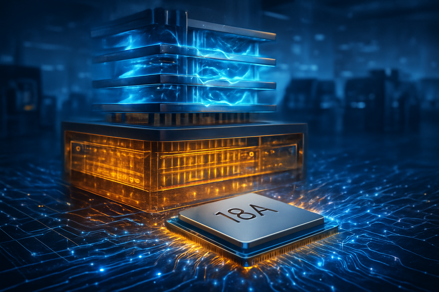
The N2 Leap: GAAFET and the End of the FinFET Era
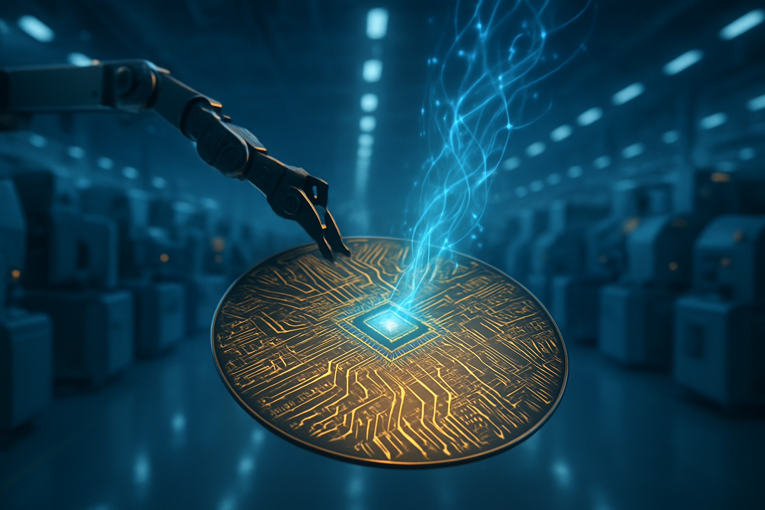
The transition to the N2 node represents TSMC’s most significant architectural shift in over a decade. After years of refining the FinFET (Fin Field-Effect Transistor) structure, the foundry is officially moving to Gate-All-Around FET (GAAFET) technology, specifically utilizing a nanosheet architecture. In this design, the gate surrounds the channel on all four sides, providing vastly superior electrostatic control. This technical pivot is essential for maintaining the pace of Moore’s Law, as it significantly reduces current leakage—a primary obstacle in the sub-3nm era.
Technically, the N2 node delivers substantial gains over the current N3E (3nm) standard. Early performance metrics indicate a 10–15% speed improvement at the same power levels, or a 25–30% reduction in power consumption at the same clock speeds. Furthermore, transistor density is expected to increase by approximately 1.1x. However, this first generation of 2nm will not yet include "Backside Power Delivery"—a feature TSMC calls the "Super Power Rail." That innovation is reserved for the N2P and A16 (1.6nm) nodes, which are slated for late 2026 and 2027, respectively.
Initial reactions from the semiconductor research community have been a mix of awe and caution. While the efficiency gains of GAAFET are undeniable, the cost of entry has reached a fever pitch. Reports suggest that 2nm wafers are priced at approximately $30,000 per unit—a 50% premium over 3nm wafers. Industry experts note that while Apple can absorb these costs by positioning its A20 and M6 chips as premium offerings, smaller players may find the financial barrier to 2nm entry nearly insurmountable, potentially widening the gap between the "silicon elite" and the rest of the market.
The Capacity War: Apple’s Dominance and the Ripple Effect
Apple’s aggressive booking of over half of TSMC’s 2nm capacity for 2026 serves as a defensive moat against its competitors. By locking down the A20 chip production for the iPhone 18 series, Apple ensures it will be the first to offer consumer-grade 2nm hardware. This strategy also extends to its Mac and Vision Pro lines, with the M6 and R2 chips expected to utilize the same N2 capacity. This "buyout" strategy forces other tech giants to scramble for what remains, creating a high-stakes queue that favors those with the deepest pockets.
The implications for the AI hardware market are particularly profound. NVIDIA, which has been the primary beneficiary of the AI boom, has reportedly had to adjust its "Rubin" GPU architecture plans. While the highest-end variants of the Rubin Ultra may eventually see 2nm production, the bulk of the initial Rubin (R100) volume is expected to remain on refined 3nm nodes due to the 2nm supply constraints. Similarly, AMD is facing a tight window for its Zen 6 "Venice" processors; while AMD was among the first to tape out 2nm designs, its ability to scale those products in 2026 will be severely limited by Apple’s massive footprint at TSMC’s Hsinchu and Kaohsiung fabs.
This crunch has led to a renewed interest in secondary sourcing. Both AMD and Google (NASDAQ: GOOGL) are reportedly evaluating Samsung’s (KRX: 005930) 2nm (SF2) process as a potential alternative. However, yield concerns continue to plague Samsung, leaving TSMC as the only reliable provider for high-volume, leading-edge silicon. For startups and mid-sized AI labs, the 2nm crunch means that access to the most efficient "AI at the edge" hardware will be delayed, potentially slowing the deployment of sophisticated on-device AI models that require the power-per-watt efficiency only 2nm can provide.
Silicon Geopolitics and the AI Landscape
The 2nm capacity crunch is more than a supply chain issue; it is a reflection of the broader AI landscape's insatiable demand for compute. As AI models migrate from massive data centers to local devices—a trend often referred to as "Edge AI"—the efficiency of the underlying silicon becomes the primary differentiator. The N2 node is the first process designed from the ground up to support the power envelopes required for running multi-billion parameter models on smartphones and laptops without devastating battery life.
This development also highlights the increasing concentration of technological power. With TSMC remaining the sole provider of viable 2nm logic, the world’s most advanced AI and consumer tech roadmaps are tethered to a handful of square miles in Taiwan. While TSMC is expanding its Arizona (Fab 21) operations, high-volume 2nm production in the United States is not expected until at least 2027. This geographic concentration remains a point of concern for global supply chain resilience, especially as geopolitical tensions continue to simmer.
Comparatively, the move to 2nm feels like the "Great 3nm Scramble" of 2023, but with higher stakes. In the previous cycle, the primary driver was traditional mobile performance. Today, the driver is the "AI PC" and "AI Phone" revolution. The ability to run generative AI locally is seen as the next major growth engine for the tech industry, and the 2nm node is the essential fuel for that engine. The fact that capacity is already booked through 2026 suggests that the industry expects the AI-driven upgrade cycle to be both long and aggressive.
Looking Ahead: From N2 to the 1.4nm Frontier
As TSMC ramps up its Fab 20 in Hsinchu and Fab 22 in Kaohsiung to meet the 2nm demand, the roadmap beyond 2026 is already taking shape. The near-term focus will be the introduction of N2P, which will integrate the much-anticipated Backside Power Delivery. This refinement is expected to offer an additional 5-10% performance boost by moving the power distribution network to the back of the wafer, freeing up more space for signal routing on the front.
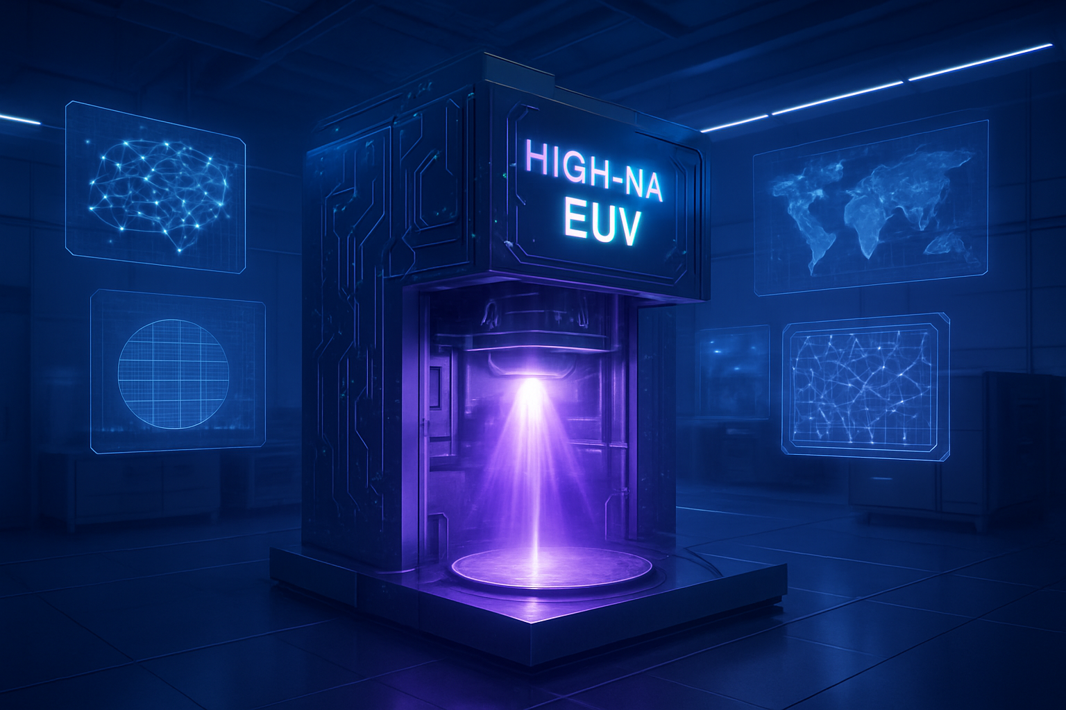
Looking further out, TSMC has already begun discussing the A14 (1.4nm) node, which is targeted for 2027 and 2028. This next frontier will likely involve High-NA (Numerical Aperture) EUV lithography, a technology that Intel (NASDAQ: INTC) has been aggressively pursuing to regain its "process leadership" crown. The competition between TSMC’s N2/A14 and Intel’s 18A/14A processes will define the next five years of semiconductor history, determining whether TSMC maintains its near-monopoly or if a more balanced ecosystem emerges.
The immediate challenge for the industry, however, remains the 2026 capacity gap. Experts predict that we may see a "tiered" market emerge, where only the most expensive flagship devices utilize 2nm silicon, while "Pro" and standard models are increasingly stratified by process node rather than just feature sets. This could lead to a longer replacement cycle for mid-range devices, as the most meaningful performance leaps are reserved for the ultra-premium tier.
Conclusion: A New Era of Scarcity
The 2nm capacity crunch at TSMC is a stark reminder that even in an era of digital abundance, the physical foundations of technology are finite. Apple’s successful maneuver to secure the majority of N2 capacity for its A20 chips gives it a formidable lead in the "AI at the edge" race, but it leaves the rest of the industry in a precarious position. For the next 24 months, the story of AI will be written as much by manufacturing yields and wafer allocations as it will be by software breakthroughs.
As we move into 2026, the primary metric to watch will be TSMC’s yield rates for the new GAAFET architecture. If the transition proves smoother than the difficult 3nm ramp, we may see additional capacity unlocked for secondary customers. However, if yields struggle, the "capacity crunch" could turn into a full-scale hardware drought, potentially delaying the next generation of AI-integrated products across the board. For now, the silicon world remains a game of musical chairs—and Apple has already claimed the best seats in the house.
This content is intended for informational purposes only and represents analysis of current AI developments.
TokenRing AI delivers enterprise-grade solutions for multi-agent AI workflow orchestration, AI-powered development tools, and seamless remote collaboration platforms.
For more information, visit https://www.tokenring.ai/.