Tag: Semiconductors

  • Oracle’s Cloud Renaissance: From Database Giant to the Nuclear-Powered Engine of the AI Supercycle

    Oracle’s Cloud Renaissance: From Database Giant to the Nuclear-Powered Engine of the AI Supercycle

    Oracle (NYSE: ORCL) has orchestrated one of the most significant pivots in corporate history, transforming from a legacy database provider into the indispensable backbone of the global artificial intelligence infrastructure. As of December 19, 2025, the company has cemented its position as the primary engine for the world's most ambitious AI projects, driven by a series of high-stakes partnerships with OpenAI, Microsoft (NASDAQ: MSFT), and Google (NASDAQ: GOOGL), alongside a definitive resolution to the TikTok "Project Texas" saga.

    This strategic evolution is not merely a software play; it is a massive driver of hardware demand that has fundamentally reshaped the semiconductor landscape. By committing tens of billions of dollars to next-generation hardware and pioneering "Sovereign AI" clouds for nation-states, Oracle has become the critical link between silicon manufacturers like NVIDIA (NASDAQ: NVDA) and the frontier models that are defining the mid-2020s.

    The Zettascale Frontier: Engineering the World’s Largest AI Clusters

    At the heart of Oracle’s recent surge is the technical prowess of Oracle Cloud Infrastructure (OCI). In late 2025, Oracle unveiled its Zettascale10 architecture, a specialized AI supercluster designed to scale to an unprecedented 131,072 NVIDIA Blackwell GPUs in a single cluster. This system delivers a staggering 16 zettaFLOPS of peak AI performance, utilizing a custom RDMA over Converged Ethernet (RoCE v2) architecture known as Oracle Acceleron. This networking stack provides 3,200 Gb/sec of cluster bandwidth with sub-2 microsecond latency, a technical feat that allows tens of thousands of GPUs to operate as a single, unified computer.

    To mitigate the industry-wide supply constraints of NVIDIA’s Blackwell chips, Oracle has aggressively diversified its hardware portfolio. In October 2025, the company announced a massive deployment of 50,000 AMD (NASDAQ: AMD) Instinct MI450 GPUs, scheduled to come online in 2026. This move, combined with the launch of the first publicly available superclusters powered by AMD’s MI300X and MI355X chips, has positioned Oracle as the leading multi-vendor AI cloud. Industry experts note that Oracle’s "bare metal" approach—providing direct access to hardware without the overhead of traditional virtualization—gives it a distinct performance advantage for training the massive parameters required for frontier models.

    A New Era of "Co-opetition": The Multicloud and OpenAI Mandate

    Oracle’s strategic positioning is perhaps best illustrated by its role in the "Stargate" initiative. In a landmark $300 billion agreement signed in mid-2025, Oracle became the primary infrastructure provider for OpenAI, committing to develop 4.5 gigawatts of data center capacity over the next five years. This deal underscores a shift in the tech ecosystem where former rivals now rely on Oracle’s specialized OCI capacity to handle the sheer scale of modern AI training. Microsoft, while a direct competitor in cloud services, has increasingly leaned on Oracle to provide the specialized OCI clusters necessary to keep pace with OpenAI’s compute demands.

    Furthermore, Oracle has successfully dismantled the "walled gardens" of the cloud industry through its Oracle Database@AWS, @Azure, and @Google Cloud initiatives. By placing its hardware directly inside rival data centers, Oracle has enabled seamless multicloud workflows. This allows enterprises to run their core Oracle data on OCI hardware while leveraging the AI tools of Amazon (NASDAQ: AMZN) or Google. This "co-opetition" model has turned Oracle into a neutral Switzerland of the cloud, benefiting from the growth of its competitors while simultaneously capturing the high-margin infrastructure spend associated with AI.

    Sovereign AI and the TikTok USDS Joint Venture

    Beyond commercial partnerships, Oracle has pioneered the concept of "Sovereign AI"—the idea that nation-states must own and operate their AI infrastructure to ensure data security and cultural alignment. Oracle has secured multi-billion dollar sovereign cloud deals with the United Kingdom, Saudi Arabia, Japan, and NATO. These deals involve building physically isolated data centers that run Oracle’s full cloud stack, providing countries with the compute power needed for national security and economic development without relying on foreign-controlled public clouds.

    This focus on data sovereignty culminated in the December 2025 resolution of the TikTok hosting agreement. ByteDance has officially signed binding agreements to form TikTok USDS Joint Venture LLC, a new U.S.-based entity majority-owned by American investors including Oracle, Silver Lake, and MGX. Oracle holds a 15% stake in the new venture and serves as the "trusted technology provider." Under this arrangement, Oracle not only hosts all U.S. user data but also oversees the retraining of TikTok’s recommendation algorithm on purely domestic data. This deal, scheduled to close in January 2026, serves as a blueprint for how AI infrastructure providers can mediate geopolitical tensions through technical oversight.

    Powering the Future: Nuclear Reactors and $100 Billion Models

    Looking ahead, Oracle is addressing the most significant bottleneck in AI: power. During recent earnings calls, Chairman Larry Ellison revealed that Oracle is designing a gigawatt-plus data center campus in Abilene, Texas, which has already secured permits for three small modular nuclear reactors (SMRs). This move into nuclear energy highlights the extreme energy requirements of future AI models. Ellison has publicly stated that the "entry price" for a competitive frontier model has risen to approximately $100 billion, a figure that necessitates the kind of industrial-scale energy and hardware integration that Oracle is currently building.

    The near-term roadmap for Oracle includes the deployment of the NVIDIA GB200 NVL72 liquid-cooled racks, which are expected to become the standard for OCI’s high-end AI offerings throughout 2026. As the demand for "Inference-as-a-Service" grows, Oracle is also expected to expand its edge computing capabilities, bringing AI processing closer to the source of data in factories, hospitals, and government offices. The primary challenge remains the global supply chain for high-end semiconductors and the regulatory hurdles associated with nuclear power, but Oracle’s massive capital expenditure—projected at $50 billion for the 2025/2026 period—suggests a full-throttle commitment to this path.

    The Hardware Supercycle: Key Takeaways

    Oracle’s transformation is a testament to the fact that the AI revolution is as much a hardware and energy story as it is a software one. By securing the infrastructure for the world’s most popular social media app, the most prominent AI startup, and several of the world’s largest governments, Oracle has effectively cornered the market on high-performance compute capacity. The "Oracle Effect" is now a primary driver of the semiconductor supercycle, keeping order books full for NVIDIA and AMD for years to come.

    As we move into 2026, the industry will be watching the closing of the TikTok USDS deal and the first milestones of the Stargate project. Oracle’s ability to successfully integrate nuclear power into its data center strategy will likely determine whether it can maintain its lead in the "battle for technical supremacy." For now, Oracle has proven that in the age of AI, the company that controls the most efficient and powerful hardware clusters holds the keys to the kingdom.


    This content is intended for informational purposes only and represents analysis of current AI developments.

    TokenRing AI delivers enterprise-grade solutions for multi-agent AI workflow orchestration, AI-powered development tools, and seamless remote collaboration platforms.
    For more information, visit https://www.tokenring.ai/.

  • Powering the AI Infrastructure: Texas Instruments Ramps Up Sherman Fab to Secure Global Supply Chains

    Powering the AI Infrastructure: Texas Instruments Ramps Up Sherman Fab to Secure Global Supply Chains

    On December 17, 2025, Texas Instruments (NASDAQ: TXN) officially commenced production at its first massive 300mm semiconductor wafer fabrication plant in Sherman, Texas. This milestone, occurring just days ago, marks a pivotal shift in the global AI hardware landscape. While the world’s attention has been fixated on the high-end GPUs that train large language models, the "SM1" facility in Sherman has begun churning out the foundational analog and embedded processing chips that serve as the essential nervous system and power delivery backbone for the next generation of AI data centers.

    The ramping up of the Sherman "mega-site" represents a $40 billion long-term commitment to domestic manufacturing, positioning Texas Instruments as a critical anchor in the U.S. semiconductor supply chain. As AI workloads demand unprecedented levels of power density and signal integrity, the chips produced at this facility—ranging from sophisticated voltage regulators to real-time controllers—are designed to ensure that the massive energy requirements of AI accelerators are met with maximum efficiency and minimal downtime.

    Technical Specifications and the 300mm Advantage

    The SM1 facility is the first of four planned "mega-fabs" at the Sherman site, specializing in the production of 300mm (12-inch) wafers. Technically, this transition from the industry-standard 200mm wafers to 300mm is a game-changer for analog manufacturing. By utilizing the larger surface area, TI can produce approximately 2.3 times more chips per wafer, effectively slashing chip-level fabrication costs by an estimated 40%. Unlike the leading-edge logic foundries that focus on sub-5nm processes, Sherman focuses on "foundational" nodes between 45nm and 130nm. These nodes are optimized for high-voltage precision and extreme durability, which are critical for the power management integrated circuits (PMICs) that regulate the 700W to 1000W+ power draws of modern AI GPUs.

    A standout technical achievement of the Sherman ramp-up is the production of advanced multiphase controllers and smart power stages, such as the CSD965203B. These components are engineered for the new 800VDC data center architectures that are becoming standard for megawatt-scale AI clusters. By shifting from traditional 48V to 800V power delivery, TI’s chips help minimize energy loss across the rack, a necessity as AI energy consumption continues to skyrocket. Furthermore, the facility is producing Sitara AM6x and C2000 series embedded processors, which provide the low-latency, real-time control required for edge AI applications, where processing happens locally on the factory floor or within autonomous systems.

    Initial reactions from industry experts have been largely positive regarding the site's scale, though financial analysts from firms like Goldman Sachs (NYSE: GS) and Morgan Stanley (NYSE: MS) have noted the significant capital expenditure required. However, the consensus among hardware engineers is that TI’s "own-and-operate" strategy provides a level of supply chain predictability that is currently unmatched. By bringing 95% of its manufacturing in-house by 2030, TI is decoupling itself from the capacity constraints of external foundries, a move that experts at Gartner describe as a "strategic masterstroke" for long-term market dominance in the analog sector.

    Market Positioning and Competitive Implications

    The ramping of Sherman creates a formidable competitive moat for Texas Instruments, particularly against its primary rival, Analog Devices (NASDAQ: ADI). While ADI has traditionally focused on high-margin, specialized chips using a hybrid manufacturing model, TI is leveraging the Sherman site to win the "commoditization war" through sheer scale and cost leadership. By mass-producing high-performance analog components at a lower cost point, TI is positioned to become the preferred "low-cost anchor" for tech giants like NVIDIA (NASDAQ: NVDA) and Apple (NASDAQ: AAPL), who require massive volumes of reliable power management silicon.

    NVIDIA, in particular, stands to benefit significantly. The two companies have reportedly collaborated on power-management solutions specifically tailored for the 800VDC architectures of NVIDIA’s latest AI supercomputers. As AI server analog IC market revenues are projected to hit $2 billion this year, TI’s ability to supply these parts in-house gives it a strategic advantage over competitors who may face lead-time issues or higher production costs. This vertical integration allows TI to offer more aggressive pricing while maintaining healthy margins, potentially forcing competitors to either accelerate their own 300mm transitions or cede market share in the high-volume data center segment.

    For startups and smaller AI labs, the increased supply of foundational chips means more stable pricing and better availability for the custom hardware rigs used in specialized AI research. The disruption here isn't in the AI models themselves, but in the physical availability of the hardware needed to run them. TI’s massive capacity ensures that the "supporting cast" of chips—the voltage regulators and signal converters—won't become the bottleneck that slows down the deployment of new AI clusters.

    Geopolitical Significance and the Broader AI Landscape

    The Sherman fab is more than just a factory; it is a centerpiece of the broader U.S. effort to reclaim "technological sovereignty" in the semiconductor space. Supported by $1.6 billion in direct funding from the CHIPS and Science Act, along with up to $8 billion in tax credits, the site is a flagship for the revitalization of the "Silicon Prairie." This development fits into a global trend where nations are racing to secure their hardware supply chains against geopolitical instability, ensuring that the components necessary for AI—the most transformative technology of the decade—are manufactured domestically.

    Comparing this to previous AI milestones, if the debut of ChatGPT was the "software moment" of the AI revolution, the ramping of Sherman is a critical part of the "infrastructure moment." We are moving past the era of experimental AI and into the era of industrial-scale deployment. This shift brings with it significant concerns regarding energy consumption and environmental impact. While TI’s chips make power delivery more efficient, the sheer scale of the data centers they support remains a point of contention for environmental advocates. However, TI has addressed some of these concerns by designing the Sherman site to meet LEED Gold standards for structural efficiency and sustainable manufacturing.

    The significance of this facility also lies in its impact on the labor market. The Sherman site already supports approximately 3,000 direct jobs, creating a new hub for high-tech manufacturing in North Texas. This regional economic boost serves as a blueprint for how the AI boom can drive growth in sectors far beyond software engineering, reaching into construction, chemical engineering, and logistics.

    Future Developments and Edge AI Horizons

    Looking ahead, the Sherman site is only at the beginning of its journey. While SM1 is now operational, the exterior shell of SM2 is already complete, with cleanroom installation and tooling expected to begin in 2026. As demand for AI-driven automation and electric vehicles continues to rise, TI plans to eventually activate SM3 and SM4, bringing the total output of the complex to over 100 million chips per day by the early 2030s.

    On the horizon, we can expect to see TI’s Sherman-produced chips integrated into more sophisticated Edge AI applications. This includes autonomous factory robots that require millisecond-level precision and medical devices that use AI to monitor patient vitals in real-time. The challenge for TI will be maintaining its technological edge as power requirements for AI chips continue to evolve. Experts predict that the next frontier will be "lateral power delivery," where power management components are integrated even more closely with the GPU to reduce thermal throttling and increase performance—a field where TI’s 300mm precision will be vital.

    Summary and Long-Term Impact

    The ramping of the Texas Instruments Sherman fab is a landmark event in the history of AI infrastructure. It signals the transition of AI from a niche research field into a globally integrated industrial powerhouse. By securing the supply of foundational analog and embedded processing chips, TI has not only fortified its own market position but has also provided the essential hardware stability required for the continued growth of the AI industry.

    The key takeaway for the industry is clear: the AI revolution will be built on silicon, and the most successful players will be those who control their own production destiny. In the coming weeks and months, watch for TI’s quarterly earnings to reflect the initial revenue gains from SM1, and keep an eye on how competitors respond to TI’s aggressive 300mm expansion. The "Silicon Prairie" is now officially online, and it is powering the future of intelligence.


    This content is intended for informational purposes only and represents analysis of current AI developments.

    TokenRing AI delivers enterprise-grade solutions for multi-agent AI workflow orchestration, AI-powered development tools, and seamless remote collaboration platforms.
    For more information, visit https://www.tokenring.ai/.
  • The Silent Architects of Intelligence: Why Semiconductor Manufacturing Stocks Defined the AI Era in 2025

    The Silent Architects of Intelligence: Why Semiconductor Manufacturing Stocks Defined the AI Era in 2025

    As 2025 draws to a close, the narrative surrounding artificial intelligence has undergone a fundamental shift. While the previous two years were defined by the meteoric rise of generative AI software and the viral success of large language models, 2025 has been the year of the "Mega-Fab." The industry has moved beyond debating the capabilities of chatbots to the grueling, high-stakes reality of physical production. In this landscape, the "picks and shovels" of the AI revolution—the semiconductor manufacturing and equipment companies—have emerged as the true power brokers of the global economy.

    The significance of these manufacturing giants cannot be overstated. As of December 19, 2025, global semiconductor sales have hit a record-breaking $697 billion, driven almost entirely by the insatiable demand for AI-grade silicon. While chip designers capture the headlines, it is the companies capable of manipulating matter at the atomic scale that have dictated the pace of AI progress this year. From the rollout of 2nm process nodes to the deployment of High-NA EUV lithography, the physical constraints of manufacturing are now the primary frontier of artificial intelligence.

    Atomic Precision: The Technical Triumph of 2nm and High-NA EUV

    The technical milestone of 2025 has undoubtedly been the successful volume production of the 2nm (N2) process node by Taiwan Semiconductor Manufacturing Company (NYSE: TSM). After years of development, TSMC confirmed this quarter that yield rates at its Baoshan and Kaohsiung facilities have exceeded 70%, a feat many analysts thought impossible by this date. This new node utilizes Gate-All-Around (GAA) transistor architecture, which provides a significant leap in energy efficiency and performance over the previous FinFET designs. For AI, this translates to chips that can process more parameters per watt, a critical metric as data center power consumption reaches critical levels.

    Supporting this transition is the mass deployment of High-NA (Numerical Aperture) Extreme Ultraviolet (EUV) lithography systems. ASML (NASDAQ: ASML) solidified its monopoly on this front in 2025, completing shipments of the Twinscan EXE:5200B to key partners. These machines, costing over $350 million each, allow for a higher resolution in chip printing, enabling the industry to push toward the 1.4nm (14A) threshold. Unlike previous lithography generations, High-NA EUV eliminates the need for complex multi-patterning, streamlining the manufacturing process for the ultra-dense processors required for next-generation AI training.

    Furthermore, the role of materials engineering has taken center stage. Applied Materials (NASDAQ: AMAT) has maintained a dominant 18% market share in wafer fabrication equipment by pioneering new techniques in Backside Power Delivery (BPD). By moving power wiring to the underside of the silicon wafer, companies like Applied Materials have solved the "routing congestion" that plagued earlier AI chip designs. This technical shift, combined with advanced "Chip on Wafer on Substrate" (CoWoS) packaging, has allowed manufacturers to stack logic and memory with unprecedented density, effectively breaking the memory wall that previously throttled AI performance.

    The Infrastructure Moat: Market Impact and Strategic Advantages

    The market performance of these manufacturing stocks in 2025 reflects their role as the backbone of the industry. While Nvidia (NASDAQ: NVDA) remains a central figure, its growth has stabilized as the market recognizes that its success is entirely dependent on the production capacity of its partners. In contrast, equipment and memory providers have seen explosive growth. Micron Technology (NASDAQ: MU), for instance, has surged 141% year-to-date, fueled by its dominance in HBM3e (High-Bandwidth Memory), which is essential for feeding data to AI GPUs at light speed.

    This shift has created a formidable "infrastructure moat" for established players. The sheer capital intensity required to compete at the 2nm level—estimated at over $25 billion per fab—has effectively locked out new entrants and even put pressure on traditional giants. While Intel (NASDAQ: INTC) has made significant strides in reaching parity with its 18A process in Arizona, the competitive advantage remains with those who control the equipment supply chain. Companies like Lam Research (NASDAQ: LRCX), which specializes in the etching and deposition processes required for 3D chip stacking, have seen their order backlogs swell to record highs as every major foundry races to expand capacity.

    The strategic advantage has also extended to the "plumbing" of the AI era. Vertiv Holdings (NYSE: VRT) has become a surprise winner of 2025, providing the liquid cooling systems necessary for the high-heat environments of AI data centers. As the industry moves toward massive GPU clusters, the ability to manage power and heat has become as valuable as the chips themselves. This has led to a broader market realization: the AI revolution is not just a software race, but a massive industrial mobilization that favors companies with deep expertise in physical engineering and logistics.

    Geopolitics and the Global Silicon Landscape

    The wider significance of these developments is deeply intertwined with global geopolitics and the "reshoring" of technology. Throughout 2025, the implementation of the CHIPS Act in the United States and similar initiatives in Europe have begun to bear fruit, with new leading-edge facilities coming online in Arizona, Ohio, and Germany. However, this transition has not been without friction. U.S. export restrictions have forced companies like Applied Materials and Lam Research to pivot away from the Chinese market, which previously accounted for a significant portion of their revenue.

    Despite these challenges, the broader AI landscape has benefited from a more diversified supply chain. The move toward domestic manufacturing has mitigated some of the risks associated with regional instability, though TSMC’s dominance in Taiwan remains a focal point of global economic security. The "Picks and Shovels" companies have acted as a stabilizing force, providing the standardized tools and materials that allow for a degree of interoperability across different foundries and regions.

    Comparing this to previous milestones, such as the mobile internet boom or the rise of cloud computing, the AI era is distinct in its demand for sheer physical scale. We are no longer just shrinking transistors; we are re-engineering the very way data moves through matter. This has raised concerns regarding the environmental impact of such a massive industrial expansion. The energy required to run these "Mega-Fabs" and the data centers they supply has forced a renewed focus on sustainability, leading to innovations in low-power silicon and more efficient manufacturing processes that were once considered secondary priorities.

    The Horizon: Silicon Photonics and the 1nm Roadmap

    Looking ahead to 2026 and beyond, the industry is already preparing for the next major leap: silicon photonics. This technology, which uses light instead of electricity to transmit data between chips, is expected to solve the interconnect bottlenecks that currently limit the size of AI clusters. Experts predict that companies like Lumentum (NASDAQ: LITE) and Fabrinet (NYSE: FN) will become the next tier of essential manufacturing stocks as optical interconnects move from niche applications to the heart of the AI data center.

    The roadmap toward 1nm and "sub-angstrom" manufacturing is also becoming clearer. While the technical challenges of quantum tunneling and heat dissipation become more acute at these scales, the collaboration between ASML, TSMC, and Applied Materials suggests that the "Moore’s Law is Dead" narrative may once again be premature. The next two years will likely see the first pilot lines for 1.4nm production, utilizing even more advanced High-NA EUV techniques and new 2D materials like molybdenum disulfide to replace traditional silicon channels.

    However, challenges remain. The talent shortage in semiconductor engineering continues to be a bottleneck, and the inflationary pressure on raw materials like neon and rare earth elements poses a constant threat to margins. As we move into 2026, the focus will likely shift toward "software-defined manufacturing," where AI itself is used to optimize the yields and efficiency of the fabs that create it, creating a virtuous cycle of silicon-driven intelligence.

    A New Era of Industrial Intelligence

    The story of AI in 2025 is the story of the factory floor. The companies profiled here—TSMC, Applied Materials, ASML, and their peers—have proven that the digital future is built on a physical foundation. Their ability to deliver unprecedented precision at a global scale has enabled the current AI boom and will dictate the limits of what is possible in the years to come. The "picks and shovels" are no longer just supporting actors; they are the lead protagonists in the most significant technological shift of the 21st century.

    As we look toward the coming weeks, investors and industry watchers should keep a close eye on the Q4 earnings reports of the major equipment manufacturers. These reports will serve as a bellwether for the 2026 capital expenditure plans of the world’s largest tech companies. If the current trend holds, the "Mega-Fab" era is only just beginning, and the silent architects of intelligence will continue to be the most critical stocks in the global market.


    This content is intended for informational purposes only and represents analysis of current AI developments.

    TokenRing AI delivers enterprise-grade solutions for multi-agent AI workflow orchestration, AI-powered development tools, and seamless remote collaboration platforms.
    For more information, visit https://www.tokenring.ai/.
  • The Great AI Rotation: Why Wall Street is Doubling Down on the Late 2025 Rebound

    The Great AI Rotation: Why Wall Street is Doubling Down on the Late 2025 Rebound

    As 2025 draws to a close, the financial markets are witnessing a powerful resurgence in artificial intelligence investments, marking a definitive end to the "valuation reckoning" that characterized the middle of the year. After a volatile summer and early autumn where skepticism over return on investment (ROI) and energy bottlenecks led to a cooling of the AI trade, a "Second Wave" of capital is now flooding back into megacap technology and semiconductor stocks. This late-year rally is fueled by a shift from experimental generative models to autonomous agentic systems and a new generation of hardware that promises to shatter previous efficiency ceilings.

    The current market environment, as of December 19, 2025, reflects a sophisticated rotation. Investors are no longer merely betting on the promise of AI; they are rewarding companies that have successfully transitioned from the "training phase" to the "utility phase." With the Federal Reserve recently pivoting toward a more accommodative monetary policy—cutting interest rates to a target range of 3.50%–3.75%—the liquidity needed to sustain massive capital expenditure projects has returned, providing a tailwind for the industry’s giants as they prepare for a high-growth 2026.

    The Rise of Agentic AI and the Rubin Era

    The technical catalyst for this rebound lies in the maturation of Agentic AI and the accelerated hardware roadmap from industry leaders. Unlike the chatbots of 2023 and 2024, the agentic systems of late 2025 are autonomous entities capable of executing complex, multi-step workflows—such as supply chain optimization, autonomous software engineering, and real-time legal auditing—without constant human intervention. Industry data suggests that nearly 40% of enterprise workflows now incorporate some form of agentic component, providing the quantifiable ROI that skeptics claimed was missing earlier this year.

    On the hardware front, NVIDIA (NASDAQ: NVDA) has effectively silenced critics with the successful ramp-up of its Blackwell Ultra (GB300) platform and the formal unveiling of the Vera Rubin (R100) architecture. The Rubin chips, built on TSMC (NYSE: TSM) advanced 2nm process and utilizing HBM4 (High Bandwidth Memory 4), represent a generational leap. Technical specifications indicate a 3x increase in compute efficiency compared to the Blackwell series, addressing the critical energy constraints that plagued data centers during the mid-year cooling period. This hardware evolution allows for significantly lower power consumption per token, making large-scale inference economically viable for a broader range of industries.

    The AI research community has reacted with notable enthusiasm to these developments, particularly the integration of "reasoning-at-inference" capabilities within the latest models. By shifting the focus from simply scaling parameters to optimizing the "thinking time" of models during execution, companies are seeing a drastic reduction in the cost of intelligence. This shift has moved the goalposts from raw training power to efficient, high-speed inference, a transition that is now being reflected in the stock prices of the entire semiconductor supply chain.

    Strategic Dominance: How the Giants are Positioning for 2026

    The rebound has solidified the market positions of the "Magnificent Seven" and their semiconductor partners, though the competitive landscape has evolved. NVIDIA has reclaimed its dominance, recently crossing the $5 trillion market capitalization milestone as Blackwell sales exceeded $11 billion in its inaugural quarter. By moving to a relentless yearly release cadence, the company has stayed ahead of internal silicon projects from its largest customers. Meanwhile, TSMC has raised its revenue guidance to mid-30% growth for the year, driven by "insane" demand for 2nm wafers from both Apple (NASDAQ: AAPL) and NVIDIA.

    Microsoft (NASDAQ: MSFT) and Alphabet (NASDAQ: GOOGL) have successfully pivoted their strategies to emphasize "Agentic Engines." Microsoft’s Copilot Studio has evolved into a platform where businesses build entire autonomous departments, helping the company boast a commercial cloud backlog of over $400 billion. Alphabet, once perceived as a laggard in the AI race, has leveraged its vertical integration with Gemini 2.0 and its proprietary TPU (Tensor Processing Unit) clusters, which now account for approximately 10% of the total AI accelerator market. This self-reliance has allowed Alphabet to maintain higher margins than competitors who are solely dependent on merchant silicon.

    Meta (NASDAQ: META) has also emerged as a primary beneficiary of the rebound. Despite an aggressive $72 billion Capex budget for 2025, the company’s focus on Llama 4 and AI-driven ad targeting has yielded record-breaking engagement metrics and stabilized operating margins. By open-sourcing its foundational models while keeping its hardware infrastructure proprietary, Meta has created a developer ecosystem that rivals the traditional cloud giants. This strategic positioning has turned what was once seen as "reckless spending" into a formidable competitive moat.

    A Global Shift in the AI Landscape

    The late 2025 rebound is more than just a stock market recovery; it represents a maturation of the global AI landscape. The "digestion phase" of mid-2025 served a necessary purpose, forcing companies to move beyond hype and focus on the physical realities of AI deployment. Energy infrastructure has become the new geopolitical currency. In regions like Northern Virginia, where power connection wait times have reached seven years, the market has begun to favor "AI-enabled revenue" stocks—companies like Oracle (NYSE: ORCL) and ServiceNow (NYSE: NOW) that are helping enterprises navigate these infrastructure bottlenecks through efficient software and decentralized data center solutions.

    This period also marks the rise of "Sovereign AI." Nations are no longer content to rely on a handful of Silicon Valley firms; instead, they are investing in domestic compute clusters. Japan’s recent $191 billion stimulus package, specifically aimed at revitalizing its semiconductor industry and AI carry trade, is a prime example of this trend. This global diversification of demand has decoupled the AI trade from purely US-centric tech sentiment, providing a more stable foundation for the current rally.

    Comparisons to previous milestones, such as the 2023 "Generative Explosion," show that the 2025 rebound is characterized by a much higher degree of institutional sophistication. The "Santa Claus Rally" of 2025 is backed by stabilizing inflation at 2.75% and a clear understanding of the "Inference Economy." While the 2023-2024 period was about building the brain, late 2025 is about putting that brain to work in the real economy.

    The Road Ahead: 2026 as the 'Year of Proof'

    Looking forward, 2026 is already being dubbed the "Year of Proof" by Wall Street analysts. The massive investments of 2025 must now translate into bottom-line operational efficiency across all sectors. We expect to see the emergence of "Sovereign AI Clouds" in Europe and the Middle East, further diversifying the revenue streams for semiconductor firms like AMD (NASDAQ: AMD) and Broadcom (NASDAQ: AVGO). The next frontier will likely be the integration of AI agents into physical robotics, bridging the gap between digital intelligence and the physical workforce.

    However, challenges remain. The "speed-to-power" bottleneck continues to be the primary threat to sustained growth. Companies that can innovate in nuclear small modular reactors (SMRs) or advanced cooling technologies will likely become the next darlings of the AI trade. Furthermore, as AI agents gain more autonomy, regulatory scrutiny regarding "agentic accountability" is expected to intensify, potentially creating new compliance hurdles for the tech giants.

    Experts predict that the market will become increasingly discerning in the coming months. The "rising tide" that lifted all AI boats in late 2025 will give way to a stock-picker's environment where only those who can prove productivity gains will continue to see valuation expansion. The focus is shifting from "growth at all costs" to "operational excellence through AI."

    Summary of the 2025 AI Rebound

    The late 2025 AI trade rebound marks a pivotal moment in technology history. It represents the transition from the speculative "Gold Rush" of training large models to the practical "Utility Era" of autonomous agents and high-efficiency inference. Key takeaways include:

    • The Shift to Agentic AI: 40% of enterprise workflows are now autonomous, providing the ROI necessary to sustain high valuations.
    • Hardware Evolution: NVIDIA’s Rubin architecture and TSMC’s 2nm process have redefined compute efficiency.
    • Macro Tailwinds: Fed rate cuts and global stimulus have revitalized liquidity in the tech sector.
    • A Discerning Market: Investors are rotating from "builders" (hardware) to "beneficiaries" (software and services) who can monetize AI effectively.

    As we move into 2026, the significance of this development cannot be overstated. The AI trade has survived its first major "bubble" scare and emerged stronger, backed by real-world utility and a more robust global infrastructure. In the coming weeks, watch for Q4 earnings reports from the hyperscalers to confirm that the "lumpy" demand of the summer has indeed smoothed out into a consistent, long-term growth trajectory.


    This content is intended for informational purposes only and represents analysis of current AI developments.

    TokenRing AI delivers enterprise-grade solutions for multi-agent AI workflow orchestration, AI-powered development tools, and seamless remote collaboration platforms.
    For more information, visit https://www.tokenring.ai/.

  • The Power Behind the Processing: OSU’s Anant Agarwal Elected to NAI for Semiconductor Breakthroughs

    The Power Behind the Processing: OSU’s Anant Agarwal Elected to NAI for Semiconductor Breakthroughs

    The National Academy of Inventors (NAI) has officially named Dr. Anant Agarwal, a Professor of Electrical and Computer Engineering at The Ohio State University (OSU), to its prestigious Class of 2025. This election marks a pivotal recognition of Agarwal’s decades-long work in wide-bandgap (WBG) semiconductors—specifically Silicon Carbide (SiC) and Gallium Nitride (GaN)—which have become the unsung heroes of the modern artificial intelligence revolution. As AI models grow in complexity, the hardware required to train and run them has hit a "power wall," and Agarwal’s innovations provide the critical efficiency needed to scale these systems sustainably.

    The significance of this development cannot be overstated as the tech industry grapples with the massive energy demands of next-generation data centers. While much of the public's attention remains on the logic chips designed by companies like NVIDIA (NASDAQ:NVDA), the power electronics that deliver electricity to those chips are often the limiting factor in performance and density. Dr. Agarwal’s election to the NAI highlights a shift in the AI hardware narrative: the most important breakthroughs are no longer just about how we process data, but how we manage the massive amounts of energy required to do so.

    Revolutionizing Power with Silicon Carbide and AI-Driven Screening

    Dr. Agarwal’s work at the SiC Power Devices Reliability Lab at OSU focuses on the "ruggedness" and reliability of Silicon Carbide MOSFETs, which are capable of operating at much higher voltages, temperatures, and frequencies than traditional silicon. A primary technical challenge in SiC technology has been the instability of the gate oxide layer, which often leads to device failure under the high-stress environments typical of AI server racks. Agarwal’s team has pioneered a threshold voltage adjustment technique using low-field pulses, effectively stabilizing the devices and ensuring they can handle the volatile power cycles of high-performance computing.

    Perhaps the most groundbreaking technical advancement from Agarwal’s lab in the 2024-2025 period is the development of an Artificial Neural Network (ANN)-based screening methodology for semiconductor manufacturing. Traditional testing methods for SiC MOSFETs often involve destructive testing or imprecise statistical sampling. Agarwal’s new approach uses machine learning to predict the Short-Circuit Withstand Time (SCWT) of individual packaged chips. This allows manufacturers to identify and discard "weak" chips that might otherwise fail after a few months in a data center, reducing field failure rates from several percentage points to parts-per-million levels.

    Furthermore, Agarwal is pushing the boundaries of "smart" power chips through SiC CMOS technology. By integrating both N-channel and P-channel MOSFETs on a single SiC die, his research has enabled power chips that can operate at voltages exceeding 600V while maintaining six times the power density of traditional silicon. This allows for a massive reduction in the physical size of power supplies, a critical requirement for the increasingly cramped environments of AI-optimized server blades.

    Strategic Impact on the Semiconductor Giants and AI Infrastructure

    The commercial implications of Agarwal’s research are already being felt across the semiconductor industry. Companies like Wolfspeed (NYSE:WOLF), where Agarwal previously served as a technical leader, stand to benefit from the increased reliability and yield of SiC wafers. As the industry moves toward 200mm wafer production, the ANN-based screening techniques developed at OSU provide a competitive edge in maintaining quality control at scale. Major power semiconductor players, including ON Semiconductor (NASDAQ:ON) and STMicroelectronics (NYSE:STM), are also closely watching these developments as they race to supply the power-hungry AI market.

    For AI giants like NVIDIA and Google (NASDAQ:GOOGL), the adoption of Agarwal’s high-density power conversion technology is a strategic necessity. Current AI GPUs require hundreds of amps of current at very low voltages (often around 1V). Converting power from the 48V or 400V DC rails of a modern data center down to the 1V required by the chip is traditionally an inefficient process that generates immense heat. By using the 3.3 kV and 1.2 kV SiC MOSFETs commercialized through Agarwal’s spin-out, NoMIS Power, data centers can achieve higher-frequency switching, which significantly reduces the size of transformers and capacitors, allowing for more compute density per rack.

    This shift disrupts the existing cooling and power delivery market. Traditional liquid cooling providers and power module manufacturers are having to pivot as SiC-based systems can operate at junction temperatures up to 200°C. This thermal resilience allows for air-cooled power modules in environments that previously required expensive and complex liquid cooling setups, potentially lowering the capital expenditure for new AI startups and mid-sized data center operators.

    The Broader AI Landscape: Efficiency as the New Frontier

    Dr. Agarwal’s innovations fit into a broader trend where energy efficiency is becoming the primary metric for AI success. For years, the industry followed "Moore’s Law" for logic, but power electronics lagged behind. We are now entering what experts call the "Second Electronics Revolution," moving from the Silicon Age to the Wide-Bandgap Age. This transition is essential for the "decarbonization" of AI; without the efficiency gains provided by SiC and GaN, the carbon footprint of global AI training would likely become ecologically and politically untenable.

    The wider significance also touches on national security and domestic manufacturing. Through his leadership in PowerAmerica, Agarwal has been instrumental in ensuring the United States maintains a robust supply chain for wide-bandgap semiconductors. As geopolitical tensions influence the semiconductor trade, the ability to manufacture high-reliability power electronics domestically at OSU and through partners like Wolfspeed provides a strategic safeguard for the U.S. tech economy.

    However, the rapid transition to SiC is not without concerns. The manufacturing process for SiC is significantly more energy-intensive and complex than for standard silicon. While Agarwal’s work improves the reliability and usage efficiency, the industry still faces a steep curve in scaling the raw material production. Comparisons are often made to the early days of the microprocessor revolution—we are currently in the "scaling" phase of power semiconductors, where the innovations of today will determine the infrastructure of the next thirty years.

    Future Horizons: Smart Chips and 3.3kV AI Rails

    Looking ahead to 2026 and beyond, the industry expects a surge in the adoption of 3.3 kV SiC MOSFETs for AI power rails. NoMIS Power’s recent launch of these devices in late 2025 is just the beginning. Near-term developments will likely focus on integrating Agarwal's ANN-based screening directly into the automated test equipment (ATE) used by global chip foundries. This would standardize "reliability-as-a-service" for any company purchasing SiC-based power modules.

    On the horizon, we may see the emergence of "autonomous power modules"—chips that use Agarwal’s SiC CMOS technology to monitor their own health and adjust their operating parameters in real-time to prevent failure. Such "self-healing" hardware would be a game-changer for edge AI applications, such as autonomous vehicles and remote satellite systems, where manual maintenance is impossible. Experts predict that the next five years will see SiC move from a "premium" alternative to the baseline standard for all high-performance computing power delivery.

    A Legacy of Innovation and the Path Forward

    Dr. Anant Agarwal’s election to the National Academy of Inventors is a well-deserved recognition of a career that has bridged the gap between fundamental physics and industrial application. From his early days at Cree to his current leadership at Ohio State, his focus on the "ruggedness" of technology has ensured that the AI revolution is built on a stable and efficient foundation. The key takeaway for the industry is clear: the future of AI is as much about the power cord as it is about the processor.

    As we move into 2026, the tech community should watch for the results of the first large-scale deployments of ANN-screened SiC modules in hyperscale data centers. If these devices deliver the promised reduction in failure rates and energy overhead, they will solidify SiC as the bedrock of the AI era. Dr. Agarwal’s work serves as a reminder that true innovation often happens in the layers of technology we rarely see, but without which the digital world would grind to a halt.


    This content is intended for informational purposes only and represents analysis of current AI developments.

    TokenRing AI delivers enterprise-grade solutions for multi-agent AI workflow orchestration, AI-powered development tools, and seamless remote collaboration platforms.
    For more information, visit https://www.tokenring.ai/.
  • The New Retail Vanguard: Why GCT Semiconductor is the Gen Z and Millennial AI Conviction Play of 2025

    The New Retail Vanguard: Why GCT Semiconductor is the Gen Z and Millennial AI Conviction Play of 2025

    As the "Silicon Surge" of 2025 reshapes the global financial landscape, a surprising contender has emerged as a favorite among the next generation of investors. GCT Semiconductor (NYSE: GCTS), a fabless designer of advanced 5G and AI-integrated chipsets, has seen a massive influx of interest from Millennial and Gen Z retail investors. This demographic, often characterized by its pursuit of high-growth "under-the-radar" technology, has pivoted away from over-saturated large-cap stocks to back GCT’s vision of decentralized, edge-based artificial intelligence.

    The immediate significance of this shift cannot be overstated. While 2024 was a transitional year for GCT as it moved away from legacy 4G products, the company’s 2025 performance has been defined by a technical renaissance. By integrating AI-driven network optimization directly into its silicon, GCT is not just providing connectivity; it is providing the intelligent infrastructure required for the next decade of autonomous systems, aviation, and satellite-to-cellular communication. For retail investors on platforms like Robinhood and Reddit, GCTS represents a rare "pure play" on the intersection of 5G, 6G, and Edge AI at an accessible entry point.

    Silicon Intelligence: The Architecture of the GDM7275X

    At the heart of GCT’s recent success is the GDM7275X, a flagship 5G System-on-Chip (SoC) that represents a departure from traditional modem design. Unlike previous generations of chipsets that relied on centralized data centers for complex processing, the GDM7275X incorporates dual 1.6GHz quad Cortex-A55 processors and dedicated AI-driven signal processing. This allows the hardware to perform real-time digital signal optimization and performance tuning directly on the device. By moving these AI capabilities to the "edge," GCT reduces latency and power consumption, making it an ideal choice for high-demand applications like Fixed Wireless Access (FWA) and industrial IoT.

    Technical experts have noted that GCT’s approach differs from competitors by focusing on "Non-Terrestrial Networks" (NTN) and high-speed mobility. In June 2025, the company successfully completed the first end-to-end 5G call for the next-generation Air-to-Ground (ATG) network of Gogo (NASDAQ: GOGO). Handling the extreme Doppler shifts and high-velocity handovers required for aviation connectivity is a feat that few silicon designers have mastered. This capability has earned GCT praise from the AI research community, which views the company’s ability to maintain stable, high-speed AI processing in extreme environments as a significant technical milestone.

    Disrupting the Giants: Strategic Partnerships and Market Positioning

    The rise of GCT Semiconductor is creating ripples across the semiconductor industry, challenging the dominance of established giants like Qualcomm (NASDAQ: QCOM) and MediaTek. While the larger players focus on the mass-market smartphone sector, GCT has carved out a lucrative niche in mission-critical infrastructure and specialized AI applications. A landmark partnership with Aramco Digital in Saudi Arabia has positioned GCTS as a primary driver of the Kingdom’s Vision 2030, focusing on localizing AI-driven 5G modem features for smart cities and industrial automation.

    This strategic positioning has significant implications for tech giants and startups alike. By collaborating with Samsung Electronics (KRX: 005930) and various European Tier One telecommunications suppliers, GCT is embedding its silicon into the backbone of global 5G infrastructure. For startups in the autonomous vehicle and drone sectors, GCT’s AI-integrated chips provide a lower-cost, high-performance alternative to the expensive hardware suites typically offered by larger vendors. The market is increasingly viewing GCTS not just as a component supplier, but as a strategic partner capable of enabling AI features that were previously restricted to high-end server environments.

    The Democratization of AI Silicon: A Broader Cultural Shift

    The popularity of GCTS among younger investors reflects a wider trend in the AI landscape: the democratization of semiconductor investment. As of late 2025, nearly 22% of Gen Z investors hold AI-specific semiconductor stocks, a statistic driven by the accessibility of financial information on TikTok and YouTube. GCT’s "2025GCT" initiative, which focused on a transparent roadmap toward 6G and satellite connectivity, became a viral talking point for creators who emphasize "value plays" over the high-valuation hype of NVIDIA (NASDAQ: NVDA).

    This shift also highlights potential concerns regarding market volatility. GCTS experienced significant price fluctuations in early 2025, dropping to a low of $0.90 before a massive recovery fueled by insider buying and the successful sampling of its 5G chipsets. This "conviction play" mentality among retail investors mirrors previous AI milestones, such as the initial surge of interest in generative AI startups in 2023. However, the difference here is the focus on hardware—the "shovels" of the AI gold rush—rather than just the software applications.

    The Road to 6G and Beyond: Future Developments

    Looking ahead, the next 12 to 24 months appear pivotal for GCT Semiconductor. The company is already deep into the development of 6G standards, leveraging its partnership with Globalstar (NYSE: GSAT) to refine "direct-to-device" satellite messaging. These NTN-capable chips are expected to become the standard for global connectivity, allowing smartphones and IoT devices to switch seamlessly between cellular and satellite networks without additional hardware.

    Experts predict that the primary challenge for GCT will be scaling its manufacturing to meet the projected revenue ramp in Q4 2025 and 2026. As 5G chipset shipments begin in earnest—carrying an average selling price roughly four times higher than legacy 4G products—GCT must manage its fabless supply chain with precision. Furthermore, the integration of even more advanced neural processing units (NPUs) into their next-generation silicon will be necessary to stay ahead of the curve as Edge AI requirements evolve from simple optimization to complex on-device generative tasks.

    Conclusion: A New Chapter in AI Infrastructure

    GCT Semiconductor’s journey from a 2024 SPAC merger to a 2025 retail favorite is a testament to the changing dynamics of the tech industry. By focusing on the intersection of AI and 5G, the company has successfully positioned itself as an essential player in the infrastructure that will power the next generation of intelligent devices. For Millennial and Gen Z investors, GCTS is more than just a stock; it is a bet on the future of decentralized intelligence and global connectivity.

    As we move into the final weeks of 2025, the industry will be watching GCT’s revenue reports closely to see if the promised "Silicon Surge" translates into long-term financial stability. With strong insider backing, high-profile partnerships, and a technical edge in the burgeoning NTN market, GCT Semiconductor has proven that even in a world dominated by tech titans, there is still plenty of room for specialized innovation to capture the market's imagination.


    This content is intended for informational purposes only and represents analysis of current AI developments.

    TokenRing AI delivers enterprise-grade solutions for multi-agent AI workflow orchestration, AI-powered development tools, and seamless remote collaboration platforms.
    For more information, visit https://www.tokenring.ai/.

  • Powering the Intelligence Explosion: Navitas Semiconductor’s 800V Revolution Redefines AI Data Centers and Electric Mobility

    Powering the Intelligence Explosion: Navitas Semiconductor’s 800V Revolution Redefines AI Data Centers and Electric Mobility

    As the world grapples with the insatiable power demands of the generative AI era, Navitas Semiconductor (Nasdaq: NVTS) has emerged as a pivotal architect of the infrastructure required to sustain it. By spearheading a transition to 800V high-voltage architectures, the company is effectively dismantling the "energy wall" that threatened to stall the deployment of next-generation AI clusters and the mass adoption of ultra-fast-charging electric vehicles.

    This technological pivot marks a fundamental shift in how electricity is managed at the edge of compute and mobility. As of December 2025, the industry has moved beyond traditional silicon-based power systems, which are increasingly seen as the bottleneck in the race for AI supremacy. Navitas’s integrated approach, combining Gallium Nitride (GaN) and Silicon Carbide (SiC) technologies, is now the gold standard for efficiency, enabling the 120kW+ server racks and 18-minute EV charging cycles that define the current technological landscape.

    The 12kW Breakthrough: Engineering the "AI Factory"

    The technical cornerstone of this revolution is Navitas’s dual-engine strategy, which pairs its GaNSafe™ and GeneSiC™ platforms to achieve unprecedented power density. In May 2025, Navitas unveiled its 12kW power supply unit (PSU), a device roughly the size of a laptop charger that delivers enough energy to power an entire residential block. Utilizing the IntelliWeave™ digital control platform, these units achieve over 97% efficiency, a critical metric when every fraction of a percentage point in energy loss translates into millions of dollars in cooling costs for hyperscale data centers.

    This advancement is a radical departure from the 54V systems that dominated the industry just two years ago. At 54V, delivering the thousands of amps required by modern GPUs like NVIDIA’s (Nasdaq: NVDA) Blackwell and the new Rubin Ultra series resulted in massive "I²R" heat losses and required thick, heavy copper busbars. By moving to an 800V High-Voltage Direct Current (HVDC) architecture—codenamed "Kyber" in Navitas’s latest collaboration with NVIDIA—the system can deliver the same power with significantly lower current. This reduces copper wiring requirements by 45% and eliminates multiple energy-sapping AC-to-DC conversion stages, allowing for more compute density within the same physical footprint.

    Initial reactions from the AI research community have been overwhelmingly positive, with engineers noting that the 800V shift is as much a thermal management breakthrough as it is a power one. By integrating sub-350ns short-circuit protection directly into the GaNSafe chips, Navitas has also addressed the reliability concerns that previously plagued high-voltage wide-bandgap semiconductors, making them viable for the mission-critical "always-on" nature of AI factories.

    Market Positioning: The Pivot to High-Margin Infrastructure

    Navitas’s strategic trajectory throughout 2025 has seen the company aggressively pivot away from low-margin consumer electronics toward the high-stakes sectors of AI, EV, and solar energy. This "Navitas 2.0" strategy has positioned the company as a direct challenger to legacy giants like Infineon Technologies (OTC: IFNNY) and STMicroelectronics (NYSE: STM). While STMicroelectronics continues to hold a strong grip on the Tesla (Nasdaq: TSLA) supply chain, Navitas has carved out a leadership position in the burgeoning 800V AI data center market, which is projected to reach $2.6 billion by 2030.

    The primary beneficiaries of this development are the "Magnificent Seven" tech giants and specialized AI cloud providers. For companies like Microsoft (Nasdaq: MSFT) and Alphabet (Nasdaq: GOOGL), the adoption of Navitas’s 800V technology allows them to pack more GPUs into existing data center shells, deferring billions in capital expenditure for new facility construction. Furthermore, Navitas’s recent partnership with Cyient Semiconductors to build a GaN ecosystem in India suggests a strategic move to diversify the global supply chain, providing a hedge against geopolitical tensions that have historically impacted the semiconductor industry.

    Competitive implications are stark: traditional silicon power chipmakers are finding themselves sidelined in the high-performance tier. As AI chips exceed the 1,000W-per-GPU threshold, the physical properties of silicon simply cannot handle the heat and switching speeds required. This has forced a consolidation in the industry, with companies like Wolfspeed (NYSE: WOLF) and Texas Instruments (Nasdaq: TXN) racing to scale their own 200mm SiC and GaN production lines to match Navitas's specialized "pure-play" efficiency.

    The Wider Significance: Breaking the Energy Wall

    The 800V revolution is more than just a hardware upgrade; it is a necessary evolution in the face of a global energy crisis. As AI compute demand is expected to consume up to 10% of global electricity by 2030, the efficiency gains provided by wide-bandgap materials like GaN and SiC have become a matter of environmental and economic survival. Navitas’s technology directly addresses the "Energy Wall," a point where the cost and heat of power delivery would theoretically cap the growth of AI intelligence.

    Comparisons are being drawn to the transition from vacuum tubes to transistors in the mid-20th century. Just as the transistor allowed for the miniaturization and proliferation of computers, 800V power semiconductors are allowing for the "physicalization" of AI—moving it from massive, centralized warehouses into more compact, efficient, and even mobile forms. However, this shift also raises concerns about the concentration of power (both literal and figurative) within the few companies that control the high-efficiency semiconductor supply chain.

    Sustainability advocates have noted that while the 800V shift saves energy, the sheer scale of AI expansion may still lead to a net increase in carbon emissions. Nevertheless, the ability to reduce copper usage by hundreds of kilograms per rack and improve EV range by 10% through GeneSiC traction inverters represents a significant step toward a more resource-efficient future. The 800V architecture is now the bridge between the digital intelligence of AI and the physical reality of the power grid.

    Future Horizons: From 800V to Grid-Scale Intelligence

    Looking ahead to 2026 and beyond, the industry expects Navitas to push the boundaries even further. The recent announcement of a 2300V/3300V Ultra-High Voltage (UHV) SiC portfolio suggests that the company is looking past the data center and toward the electrical grid itself. These devices could enable solid-state transformers and grid-scale energy storage systems that are smaller and more efficient than current infrastructure, potentially integrating renewable energy sources directly into AI data centers.

    In the near term, the focus remains on the "Rubin Ultra" generation of AI chips. Navitas has already unveiled 100V GaN FETs optimized for the point-of-load power boards that sit directly next to these processors. The challenge will be scaling production to meet the explosive demand while maintaining the rigorous quality standards required for automotive and hyperscale applications. Experts predict that the next frontier will be "Vertical Power Delivery," where power semiconductors are mounted directly beneath the AI chip to further reduce path resistance and maximize performance.

    A New Era of Power Electronics

    Navitas Semiconductor’s 800V revolution represents a definitive chapter in the history of AI development. By solving the physical constraints of power delivery, they have provided the "oxygen" for the AI fire to continue burning. The transition from silicon to GaN and SiC is no longer a future prospect—it is the present reality of 2025, driven by the dual engines of high-performance compute and the electrification of transport.

    The significance of this development cannot be overstated: without the efficiency gains of 800V architectures, the current trajectory of AI scaling would be economically and physically impossible. In the coming weeks and months, industry watchers should look for the first production-scale deployments of the 12kW "Kyber" racks and the expansion of GaNSafe technology into mainstream, affordable electric vehicles. Navitas has successfully positioned itself not just as a component supplier, but as a fundamental enabler of the 21st-century technological stack.


    This content is intended for informational purposes only and represents analysis of current AI developments.

    TokenRing AI delivers enterprise-grade solutions for multi-agent AI workflow orchestration, AI-powered development tools, and seamless remote collaboration platforms.
    For more information, visit https://www.tokenring.ai/.
  • The New Silicon Alliance: Nvidia Secures FTC Clearance for $5 Billion Intel Investment

    The New Silicon Alliance: Nvidia Secures FTC Clearance for $5 Billion Intel Investment

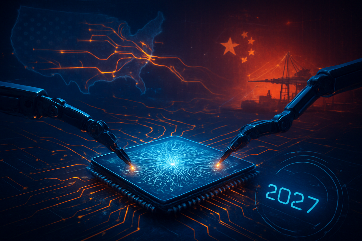
    In a move that fundamentally redraws the map of the global semiconductor industry, the Federal Trade Commission (FTC) has officially granted antitrust clearance for Nvidia (NASDAQ:NVDA) to complete its landmark $5 billion investment in Intel (NASDAQ:INTC). Announced today, December 19, 2025, the decision marks the conclusion of a high-stakes regulatory review under the Hart-Scott-Rodino Act. The deal grants Nvidia an approximately 5% stake in the legacy chipmaker, solidifying a strategic "co-opetition" model that aims to merge Nvidia’s dominance in AI acceleration with Intel’s foundational x86 architecture and domestic manufacturing capabilities.

    The significance of this clearance cannot be overstated. Following a turbulent year for Intel—which saw a 10% equity infusion from the U.S. government just months ago to stabilize its operations—this partnership provides the financial and technical "lifeline" necessary to keep the American silicon giant competitive. For the broader AI industry, the deal signals an end to the era of rigid hardware silos, as the two giants prepare to co-develop integrated platforms that could define the next decade of data center and edge computing.

    The technical core of the agreement centers on a historic integration of proprietary technologies that were previously considered incompatible. Most notably, Intel has agreed to integrate Nvidia’s high-speed NVLink interconnect directly into its future Xeon processor designs. This allows Intel CPUs to serve as seamless "head nodes" within Nvidia’s massive rack-scale AI systems, such as the Blackwell and upcoming Vera-Rubin architectures. Historically, Nvidia has pushed its own Arm-based "Grace" CPUs for these roles; by opening NVLink to Intel, the companies are creating a high-performance x86 alternative that caters to the massive installed base of enterprise software optimized for Intel’s instruction set.

    Furthermore, the collaboration introduces a new category of "System-on-Chip" (SoC) designs for the consumer and workstation markets. These chips will combine Intel’s latest x86 performance cores with Nvidia’s RTX graphics and AI tensor cores on a single die, using advanced 3D packaging. This "Intel x86 RTX" platform is specifically designed to dominate the burgeoning "AI PC" market, offering local generative AI performance that exceeds current integrated graphics solutions. Initial reports suggest these chips will utilize Intel’s PowerVia backside power delivery and RibbonFET transistor architecture, representing a significant leap in energy efficiency for AI-heavy workloads.

    Industry experts note that this differs sharply from previous "partnership" attempts, such as the short-lived Kaby Lake-G project which paired Intel CPUs with AMD graphics. Unlike that limited experiment, this deal includes deep architectural access. Nvidia will now have the ability to request custom x86 CPU designs from Intel’s Foundry division that are specifically tuned for the data-handling requirements of large language model (LLM) training and inference. Initial reactions from the research community have been cautiously optimistic, with many praising the potential for reduced latency between the CPU and GPU, though some express concern over the further consolidation of proprietary standards.

    The competitive ripples of this deal are already being felt across the globe, with Advanced Micro Devices (NASDAQ:AMD) and Taiwan Semiconductor Manufacturing Company (NYSE:TSM) facing the most immediate pressure. AMD, which has long marketed itself as the only provider of both high-end x86 CPUs and AI GPUs, now finds its unique value proposition challenged by a unified Nvidia-Intel front. Market analysts observed a 5% dip in AMD shares following the FTC announcement, as investors worry that the "Intel-Nvidia" stack will become the default standard for enterprise AI deployments, potentially squeezing AMD’s EPYC and Instinct product lines.

    For TSMC, the deal introduces a long-term strategic threat to its fabrication dominance. While Nvidia remains heavily reliant on TSMC for its current-generation 3nm and 2nm production, the investment in Intel includes a roadmap for Nvidia to utilize Intel Foundry’s 18A node as a secondary source. This move aligns with "China-plus-one" supply chain strategies and provides Nvidia with a domestic manufacturing hedge against geopolitical instability in the Taiwan Strait. If Intel can successfully execute its 18A ramp-up, Nvidia may shift significant volume away from Taiwan, altering the power balance of the foundry market.

    Startups and smaller AI labs may find themselves in a complex position. While the integration of x86 and NVLink could simplify the deployment of AI clusters by making them compatible with existing data center infrastructure, the alliance strengthens Nvidia's "walled garden" ecosystem. By embedding its proprietary interconnects into the world’s most common CPU architecture, Nvidia makes it increasingly difficult for rival AI chip startups—like Groq or Cerebras—to find a foothold in systems that are now being built around an Intel-Nvidia backbone.

    Looking at the broader AI landscape, this deal is a clear manifestation of the "National Silicon" trend that has accelerated throughout 2025. With the U.S. government already holding a 10% stake in Intel, the addition of Nvidia’s capital and R&D muscle effectively creates a "National Champion" for AI hardware. This aligns with the goals of the CHIPS and Science Act to secure the domestic supply chain for critical technologies. However, this level of concentration raises significant concerns regarding market entry for new players and the potential for price-setting in the high-end server market.

    The move also reflects a shift in AI hardware philosophy from "general-purpose" to "tightly coupled" systems. As LLMs grow in complexity, the bottleneck is no longer just raw compute power, but the speed at which data moves between the processor and memory. By merging the CPU and GPU ecosystems, Nvidia and Intel are addressing the "memory wall" that has plagued AI development. This mirrors previous industry milestones like the integration of the floating-point unit into the CPU, but on a much more massive, multi-chip scale.

    However, critics point out that this alliance could stifle the momentum of open-source hardware standards like UALink and CXL. If the two largest players in the industry double down on a proprietary NVLink-Intel integration, the dream of a truly interoperable, vendor-neutral AI data center may be deferred. The FTC’s decision to clear the deal suggests that regulators currently prioritize domestic manufacturing stability and technological leadership over the risks of reduced competition in the interconnect market.

    In the near term, the industry is waiting for the first "joint-design" silicon to tape out. Analysts expect the first Intel-manufactured Nvidia components to appear on the 18A node by early 2027, with the first integrated x86 RTX consumer chips potentially arriving for the 2026 holiday season. These products will likely target high-end "Prosumer" laptops and workstations, providing a localized alternative to cloud-based AI services. The long-term challenge will be the cultural and technical integration of two companies that have spent decades as rivals; merging their software stacks—Intel’s oneAPI and Nvidia’s CUDA—will be a monumental task.

    Beyond hardware, we may see the alliance move into the software and services space. There is speculation that Nvidia’s AI Enterprise software could be bundled with Intel’s vPro enterprise management tools, creating a turnkey "AI Office" solution for global corporations. The primary hurdle remains the successful execution of Intel’s foundry roadmap. If Intel fails to hit its 18A or 14A performance targets, the partnership could sour, leaving Nvidia to return to TSMC and Intel in an even more precarious financial state.

    The FTC’s clearance of Nvidia’s investment in Intel marks the end of the "Silicon Wars" as we knew them and the beginning of a new era of strategic consolidation. Key takeaways include the $5 billion equity stake, the integration of NVLink into x86 CPUs, and the clear intent to challenge AMD and Apple in the AI PC and data center markets. This development will likely be remembered as the moment when the hardware industry accepted that the scale required for the AI era is too vast for any one company to tackle alone.

    As we move into 2026, the industry will be watching for the first engineering samples of the "Intel-Nvidia" hybrid chips. The success of this partnership will not only determine the future of these two storied companies but will also dictate the pace of AI adoption across every sector of the global economy. For now, the "Green and Blue" alliance stands as the most formidable force in the history of computing, with the regulatory green light to reshape the future of intelligence.


    This content is intended for informational purposes only and represents analysis of current AI developments.

    TokenRing AI delivers enterprise-grade solutions for multi-agent AI workflow orchestration, AI-powered development tools, and seamless remote collaboration platforms.
    For more information, visit https://www.tokenring.ai/.

  • The $7.1 Trillion ‘Options Cliff’: AI Semiconductors Face Unprecedented Volatility in Record Triple Witching

    The $7.1 Trillion ‘Options Cliff’: AI Semiconductors Face Unprecedented Volatility in Record Triple Witching

    On December 19, 2025, the global financial markets braced for the largest derivatives expiration in history, a staggering $7.1 trillion "Options Cliff" that has sent shockwaves through the technology sector. This massive concentration of expiring contracts, coinciding with the year’s final "Triple Witching" event, has triggered a liquidity tsunami, disproportionately impacting the high-flying AI semiconductor stocks that have dominated the market narrative throughout the year. As trillions in notional value are unwound, industry leaders like Nvidia and AMD are finding themselves at the epicenter of a mechanical volatility storm that threatens to decouple stock prices from their underlying fundamental growth.

    The sheer scale of this expiration is unprecedented, representing a 20% increase over the December 2024 figures and accounting for roughly 10.2% of the entire Russell 3000 market capitalization. For the AI sector, which has been the primary engine of the S&P 500’s gains over the last 24 months, the event is more than just a calendar quirk; it is a stress test of the market's structural integrity. With $5 trillion tied to S&P 500 contracts and nearly $900 billion in individual equity options reaching their end-of-life today, the "Witching Hour" has transformed the trading floor into a high-stakes arena of gamma hedging and institutional rebalancing.

    The Mechanics of the Cliff: Gamma Squeezes and Technical Turmoil

    The technical gravity of the $7.1 trillion cliff stems from the simultaneous expiration of stock options, stock index futures, and stock index options. This "Triple Witching" forces institutional investors and market makers to engage in massive rebalancing acts. In the weeks leading up to today, the AI sector saw a massive accumulation of "call" options—bets that stock prices would continue their meteoric rise. As these stocks approached key "strike prices," market makers were forced into a process known as "gamma hedging," where they must buy underlying shares to remain delta-neutral. This mechanical buying often triggers a "gamma squeeze," artificially inflating prices regardless of company performance.

    Conversely, the market is also contending with "max pain" levels—the specific price points where the highest number of options contracts expire worthless. For NVIDIA (NASDAQ: NVDA), analysts at Goldman Sachs identified a max pain zone between $150 and $155, creating a powerful downward "gravitational pull" against its current trading price of approximately $178.40. This tug-of-war between bullish gamma squeezes and the downward pressure of max pain has led to intraday swings that veteran traders describe as "purely mechanical noise." The technical complexity is further heightened by the SKEW index, which remains at an elevated 155.4, indicating that institutional players are still paying a premium for "tail protection" against a sudden year-end reversal.

    Initial reactions from the AI research and financial communities suggest a growing concern over the "financialization" of AI technology. While the underlying demand for Blackwell chips and next-generation accelerators remains robust, the stock prices are increasingly governed by complex derivative structures rather than product roadmaps. Citigroup analysts noted that the volume during this December expiration is "meaningfully higher than any prior year," distorting traditional price discovery mechanisms and making it difficult for retail investors to gauge the true value of AI leaders in the short term.

    Semiconductor Giants Caught in the Crosshairs

    Nvidia and Advanced Micro Devices (NASDAQ: AMD) have emerged as the primary casualties—and beneficiaries—of this volatility. Nvidia, the undisputed king of the AI era, saw its stock surge 3% in early trading today as it flirted with a massive "call wall" at the $180 mark. Market makers are currently locked in a battle to "pin" the stock near these major strikes to minimize their own payout liabilities. Meanwhile, reports that the U.S. administration is reviewing a proposal to allow Nvidia to export H200 AI chips to China—contingent on a 25% "security fee"—have added a layer of fundamental optimism to the technical churn, providing a floor for the stock despite the options-driven pressure.

    AMD has experienced even more dramatic swings, with its share price jumping over 5% to trade near $211.50. This surge is attributed to a rotation within the semiconductor sector, as investors seek value in "secondary" AI plays to hedge against the extreme concentration in Nvidia. The activity around AMD’s $200 call strike has been particularly intense, suggesting that traders are repositioning for a broader AI infrastructure play that extends beyond a single dominant vendor. Other players like Micron Technology (NASDAQ: MU) have also been swept up in the mania, with Micron surging 10% following strong earnings that collided head-on with the Triple Witching liquidity surge.

    For major AI labs and tech giants, this volatility creates a double-edged sword. While high valuations provide cheap capital for acquisitions and R&D, the extreme price swings can complicate stock-based compensation and long-term strategic planning. Startups in the AI space are watching closely, as the public market's appetite for semiconductor volatility often dictates the venture capital climate for hardware-centric AI innovations. The current "Options Cliff" serves as a reminder that even the most revolutionary technology is subject to the cold, hard mechanics of the global derivatives market.

    A Perfect Storm: Macroeconomic Shocks and the 'Great Data Gap'

    The 2025 Options Cliff is not occurring in a vacuum; it is being amplified by a unique set of macroeconomic circumstances. Most notable is the "Great Data Gap," a result of a 43-day federal government shutdown that lasted from October 1 to mid-November. This shutdown left investors without critical economic indicators, such as CPI and Non-Farm Payroll data, for over a month. In the absence of fundamental data, the market has become increasingly reliant on technical triggers and derivative-driven price action, making the December Triple Witching even more influential than usual.

    Simultaneously, a surprise move by the Bank of Japan to raise interest rates to 0.75%—a three-decade high—has threatened to unwind the "Yen Carry Trade." This has forced some global hedge funds to liquidate positions in high-beta tech stocks, including AI semiconductors, to cover margin calls and rebalance portfolios. This convergence of a domestic data vacuum and international monetary tightening has turned the $7.1 trillion expiration into a "perfect storm" of volatility.

    When compared to previous AI milestones, such as the initial launch of GPT-4 or Nvidia’s first trillion-dollar valuation, the current event represents a shift in the AI narrative. We are moving from a phase of "pure discovery" to a phase of "market maturity," where the financial structures surrounding the technology are as influential as the technology itself. The concern among some economists is that this level of derivative-driven volatility could lead to a "flash crash" scenario if the gamma hedging mechanisms fail to find enough liquidity during the final hour of trading.

    The Road Ahead: Santa Claus Rally or Mechanical Reversal?

    As the market moves past the December 19 deadline, experts are divided on what comes next. In the near term, many expect a "Santa Claus" rally to take hold as the mechanical pressure of the options expiration subsides, allowing stocks to return to their fundamental growth trajectories. The potential for a policy shift regarding H200 exports to China could serve as a significant catalyst for a year-end surge in the semiconductor sector. However, the challenges of 2026 loom large, including the need for companies to prove that their massive AI infrastructure investments are translating into tangible enterprise software revenue.

    Long-term, the $7.1 trillion Options Cliff may lead to calls for increased regulation or transparency in the derivatives market, particularly concerning high-growth tech sectors. Analysts predict that "volatility as a service" will become a more prominent theme, with institutional investors seeking new ways to hedge against the mechanical swings of Triple Witching events. The focus will likely shift from hardware availability to "AI ROI," as the market demands proof that the trillions of dollars in market cap are backed by sustainable business models.

    Final Thoughts: A Landmark in AI Financial History

    The December 2025 Options Cliff will likely be remembered as a landmark moment in the financialization of artificial intelligence. It marks the point where AI semiconductors moved from being niche technology stocks to becoming the primary "liquidity vehicles" for the global financial system. The $7.1 trillion expiration has demonstrated that while AI is driving the future of productivity, it is also driving the future of market complexity.

    The key takeaway for investors and industry observers is that the underlying demand for AI remains the strongest secular trend in decades, but the path to growth is increasingly paved with technical volatility. In the coming weeks, all eyes will be on the "clearing" of these $7.1 trillion in positions and whether the market can maintain its momentum without the artificial support of gamma squeezes. As we head into 2026, the real test for Nvidia, AMD, and the rest of the AI cohort will be their ability to deliver fundamental results that can withstand the mechanical storms of the derivatives market.


    This content is intended for informational purposes only and represents analysis of current AI developments.

    TokenRing AI delivers enterprise-grade solutions for multi-agent AI workflow orchestration, AI-powered development tools, and seamless remote collaboration platforms.
    For more information, visit https://www.tokenring.ai/.

  • The Silicon Silk Road: India and the Netherlands Forge a New Semiconductor Axis for the AI Era

    The Silicon Silk Road: India and the Netherlands Forge a New Semiconductor Axis for the AI Era

    In a move that signals a tectonic shift in the global technology landscape, India and the Netherlands have today, December 19, 2025, finalized the "Silicon Silk Road" strategic alliance. This comprehensive framework, signed in New Delhi, aims to bridge the gap between European high-tech precision and Indian industrial scale. By integrating the Netherlands’ world-leading expertise in lithography and semiconductor equipment with India’s rapidly expanding manufacturing ecosystem, the partnership seeks to create a resilient, alternative supply chain for the high-performance hardware required to power the next generation of artificial intelligence.

    The immediate significance of this alliance cannot be overstated. As the global demand for AI-optimized chips—specifically those capable of handling massive large language model (LLM) training and edge computing—reaches a fever pitch, the "Silicon Silk Road" provides a blueprint for a decentralized manufacturing future. The agreement moves beyond simple trade, establishing a co-development model that includes technology transfers, joint R&D in advanced materials, and the creation of specialized maintenance hubs that will ensure India’s upcoming fabrication units (fabs) operate with the world’s most advanced Dutch-made machinery.

    Technical Foundations: Lithography, Labs, and Lab-Grown Diamonds

    The core of the alliance is built upon unprecedented commitments from Dutch semiconductor giants. NXP Semiconductors N.V. (NASDAQ:NXPI) has officially announced a massive $1 billion investment to double its research and development presence in India. This expansion is focused on the design of 5-nanometer automotive and AI chips, with a new R&D center slated for the Greater Noida Semiconductor Park. Unlike previous design-only centers, this facility will work in tandem with Indian manufacturing partners to prototype "system-on-chip" (SoC) architectures specifically optimized for low-latency AI applications.

    Simultaneously, ASML Holding N.V. (NASDAQ:ASML) is shifting its strategy from a vendor-client relationship to a deep-tier partnership. For the first time, ASML will establish "Holistic Lithography" maintenance labs within India. These labs are designed to provide real-time technical support and software calibration for the Extreme Ultraviolet (EUV) and Deep Ultraviolet (DUV) lithography systems that are essential for high-end chip production. This differs from existing models where technical expertise was centralized in Europe or East Asia, effectively removing a significant bottleneck for Indian fab operators like the Tata Group and Micron Technology, Inc. (NASDAQ:MU).

    One of the most technically ambitious aspects of the 2025 framework is the joint research into lab-grown diamonds (LGD) as a substrate for semiconductors. Leveraging India’s established diamond-processing hub in Surat and Dutch precision engineering, the partnership aims to develop diamond-based chips that can handle significantly higher thermal loads than traditional silicon. This breakthrough could revolutionize AI hardware, where heat management is currently a primary limiting factor for processing density in data centers.

    Strategic Realignment: Winners in the New Hardware Race

    The "Silicon Silk Road" creates a new competitive theater for the world’s largest AI labs and hardware providers. Companies like NVIDIA Corporation (NASDAQ:NVDA) and Advanced Micro Devices, Inc. (NASDAQ:AMD) stand to benefit immensely from a more diversified manufacturing base. By having a viable, Dutch-supported manufacturing alternative in India, these tech giants can mitigate the geopolitical risks associated with the current concentration of production in East Asia. The alliance provides a "China+1" strategy with teeth, offering a stable environment backed by European intellectual property protections and Indian production-linked incentives (PLI).

    For the Netherlands, the alliance secures a massive, long-term market for its high-tech exports at a time when global trade restrictions are tightening. ASML and NXP are effectively "future-proofing" their revenue streams by embedding themselves into the foundation of India’s digital infrastructure. Meanwhile, Indian tech conglomerates and startups are gaining access to the "holy grail" of semiconductor manufacturing: the ability to move from chip design to domestic fabrication with the support of the world’s most advanced equipment manufacturers. This positioning gives Indian firms a strategic advantage in the burgeoning field of "Sovereign AI," where nations seek to control their own computational resources.

    Geopolitics and the Global AI Landscape

    The emergence of the Silicon Silk Road fits into a broader trend of "techno-nationalism," where semiconductor self-sufficiency is viewed as a pillar of national security. This partnership is a direct response to the fragility of global supply chains exposed during the early 2020s. By forging this link, India and the Netherlands are creating a middle path that avoids the binary choice between US-led and China-led ecosystems. It is a milestone comparable to the early 2000s outsourcing boom, but with a critical difference: this time, India is moving up the value chain into the most complex manufacturing process ever devised by humanity.

    However, the alliance does not come without concerns. Industry analysts have pointed to the immense energy requirements of advanced fabs and the potential environmental impact of large-scale semiconductor manufacturing in India. Furthermore, the transfer of highly sensitive lithography technology requires a level of cybersecurity and intellectual property protection that will be a constant test for Indian regulators. Comparing this to previous milestones like the CHIPS Act, the Silicon Silk Road is unique because it relies on bilateral synergy rather than unilateral subsidies, blending Dutch technical precision with India’s demographic dividend.

    The Horizon: 2026 and Beyond

    Looking ahead, the next 24 months will be critical for the execution of the 2025 framework. The immediate goal is the operationalization of the first joint R&D labs and the commencement of training for the first cohort of 85,000 semiconductor professionals that India aims to produce by 2030. Near-term developments will likely include the announcement of a joint venture between an Indian industrial house and a Dutch equipment firm to manufacture semiconductor components—not just chips—locally, further deepening the supply chain.

    The long-term vision involves the commercialization of the lab-grown diamond substrate technology, which could place the India-Netherlands axis at the forefront of "Beyond Silicon" computing. Experts predict that by 2028, the first AI accelerators featuring "Made in India" chips, fabricated using ASML-supported systems, will hit the global market. The primary challenge will be maintaining the pace of infrastructure development—specifically stable power and ultra-pure water supplies—to match the requirements of the high-tech machinery being deployed.

    Conclusion: A New Chapter in Industrial History

    The signing of the Silicon Silk Road alliance marks the end of an era where semiconductor manufacturing was the exclusive domain of a few select geographies. It represents a maturation of India’s industrial ambitions and a strategic pivot for the Netherlands as it seeks to maintain its technological edge in an increasingly fragmented world. The key takeaway is clear: the future of AI hardware will not be determined by a single nation, but by the strength and resilience of the networks they build.

    As we move into 2026, the global tech community will be watching the progress in Greater Noida and the research labs of Eindhoven with intense interest. The success of this partnership could serve as a model for other nations looking to secure their technological future. For now, the "Silicon Silk Road" stands as a testament to the power of strategic collaboration in the age of artificial intelligence, promising to reshape the hardware that will define the rest of the 21st century.


    This content is intended for informational purposes only and represents analysis of current AI developments.

    TokenRing AI delivers enterprise-grade solutions for multi-agent AI workflow orchestration, AI-powered development tools, and seamless remote collaboration platforms.
    For more information, visit https://www.tokenring.ai/.