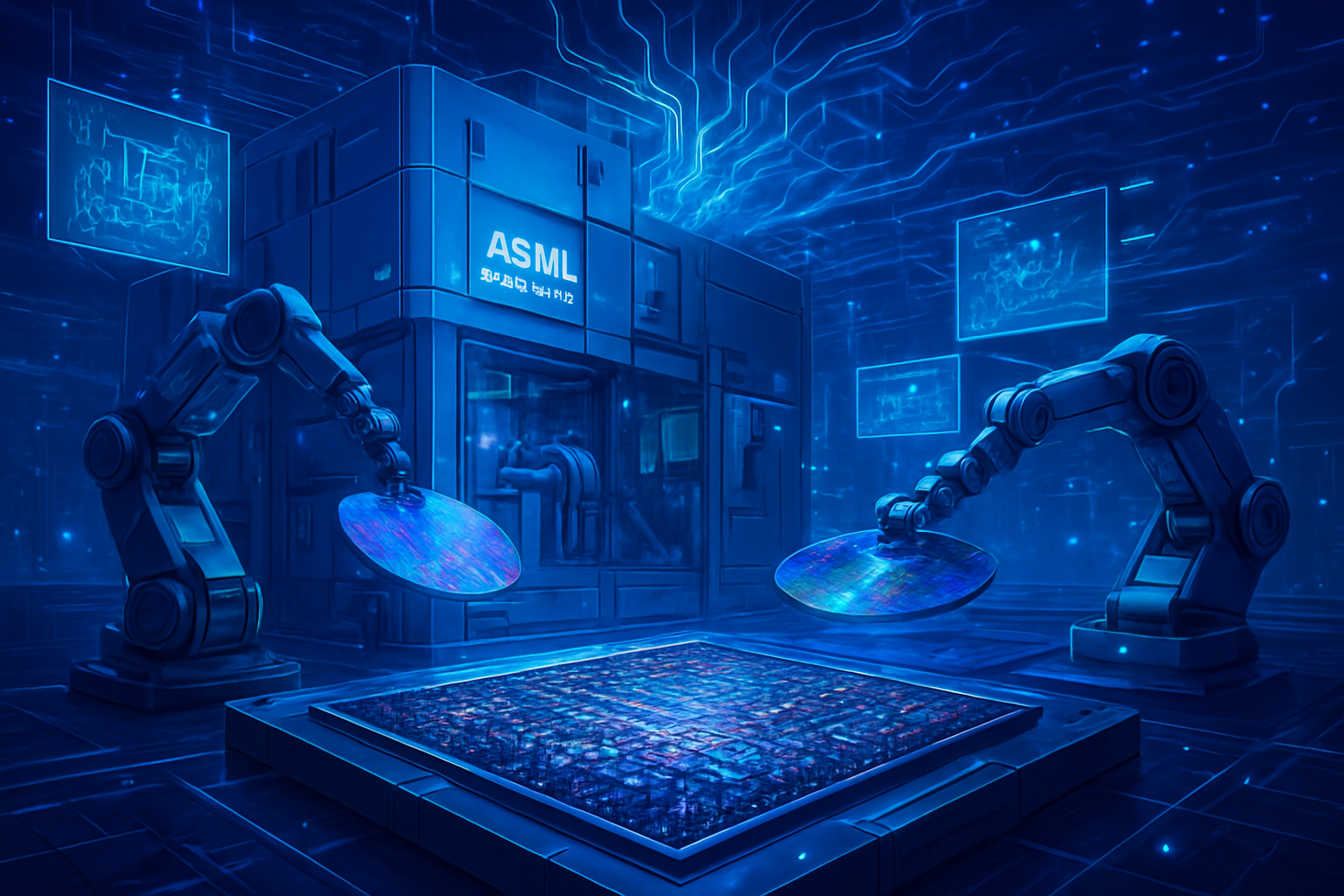
As 2025 draws to a close, the undisputed reign of NVIDIA (NASDAQ: NVDA) in the AI data center is facing its most significant structural challenge yet. While NVIDIA’s Blackwell architecture remains the gold standard for frontier model training, a parallel economy of "custom silicon" has reached a fever pitch. This week, industry reports and financial disclosures from Broadcom (NASDAQ: AVGO) have sent shockwaves through the semiconductor sector, revealing a staggering $50 billion pipeline for custom AI accelerators (XPUs) destined for the world’s largest hyperscalers.
This shift represents a fundamental "Silicon Schism" in the AI industry. On one side stands NVIDIA’s general-purpose, high-margin GPU dominance, and on the other, a growing coalition of tech giants like Google (NASDAQ: GOOGL), Microsoft (NASDAQ: MSFT), and Meta (NASDAQ: META) who are increasingly designing their own chips to bypass the "NVIDIA tax." With Broadcom acting as the primary architect for these bespoke solutions, the competitive tension between the "Swiss Army Knife" of Blackwell and the "Precision Scalpels" of custom ASICs has become the defining battle of the generative AI era.
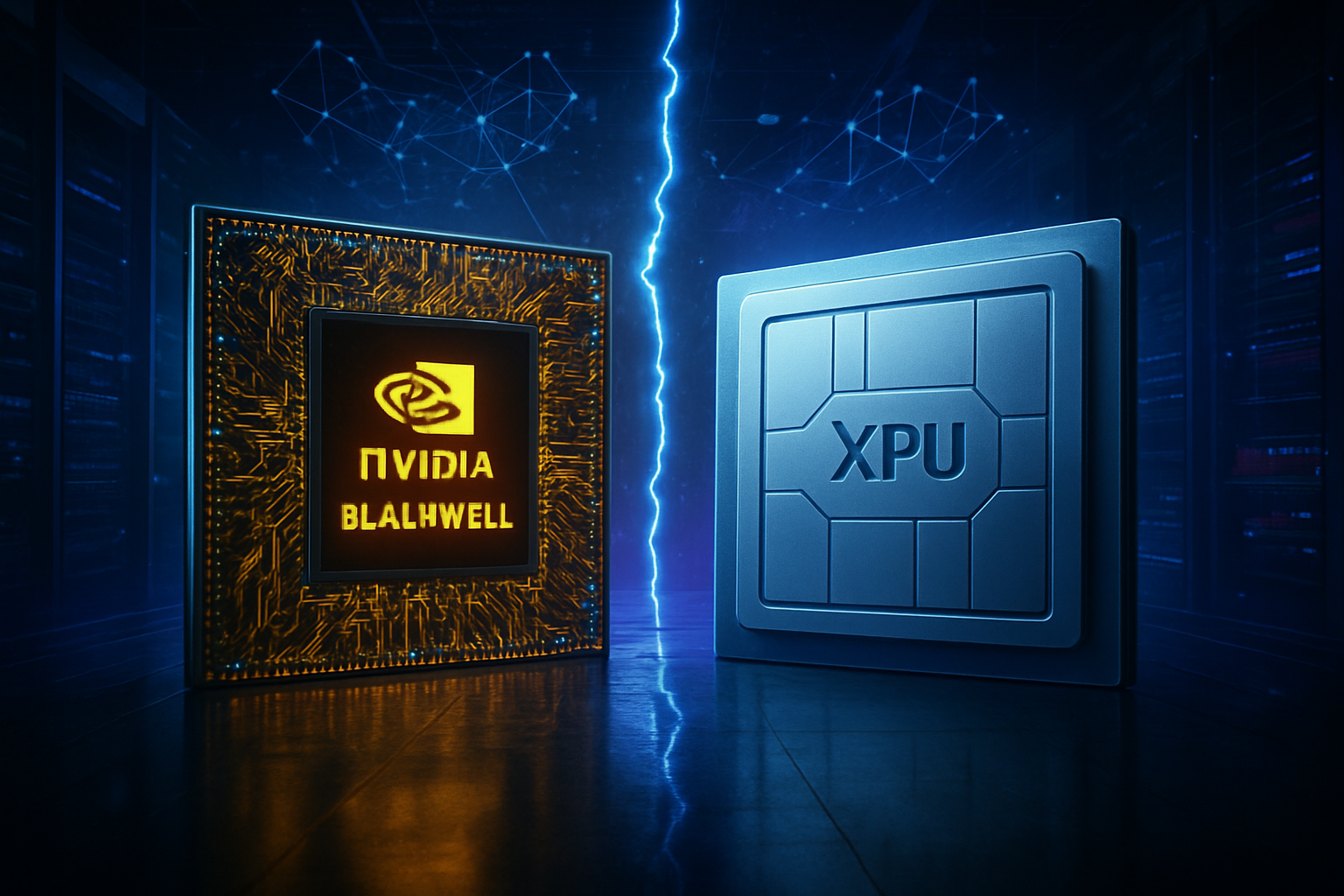
The Technical Tug-of-War: Blackwell Ultra vs. The Rise of the XPU
At the heart of this rivalry is the technical divergence between flexibility and efficiency. NVIDIA’s current flagship, the Blackwell Ultra (B300), which entered mass production in the second half of 2025, is a marvel of engineering. Boasting 288GB of HBM3E memory and delivering 15 PFLOPS of dense FP4 compute, it is designed to handle any AI workload thrown at it. However, this versatility comes at a cost—both in terms of power consumption and price. The Blackwell architecture is built to be everything to everyone, a necessity for researchers experimenting with new model architectures that haven't yet been standardized.
In contrast, the custom Application-Specific Integrated Circuits (ASICs), or XPUs, being co-developed by Broadcom and hyperscalers, are stripped-down powerhouses. By late 2025, Google’s TPU v7 and Meta’s MTIA 3 have demonstrated that for specific, high-volume tasks—particularly inference and stable Transformer-based training—custom silicon can deliver up to a 50% improvement in power efficiency (TFLOPs per Watt) compared to Blackwell. These chips eliminate the "dark silicon" or unused features of a general-purpose GPU, focusing entirely on the tensor operations that drive modern Large Language Models (LLMs).
Furthermore, the networking layer has become a critical technical battleground. NVIDIA relies on its proprietary NVLink interconnect to maintain its "moat," creating a tightly coupled ecosystem that is difficult to leave. Broadcom, however, has championed an open-standard approach, leveraging its Tomahawk 6 switching silicon to enable massive clusters of 1 million or more XPUs via high-performance Ethernet. This architectural split means that while NVIDIA offers a superior integrated "black box" solution, the custom XPU route offers hyperscalers the ability to scale their infrastructure horizontally with far more granular control over their thermal and budgetary envelopes.
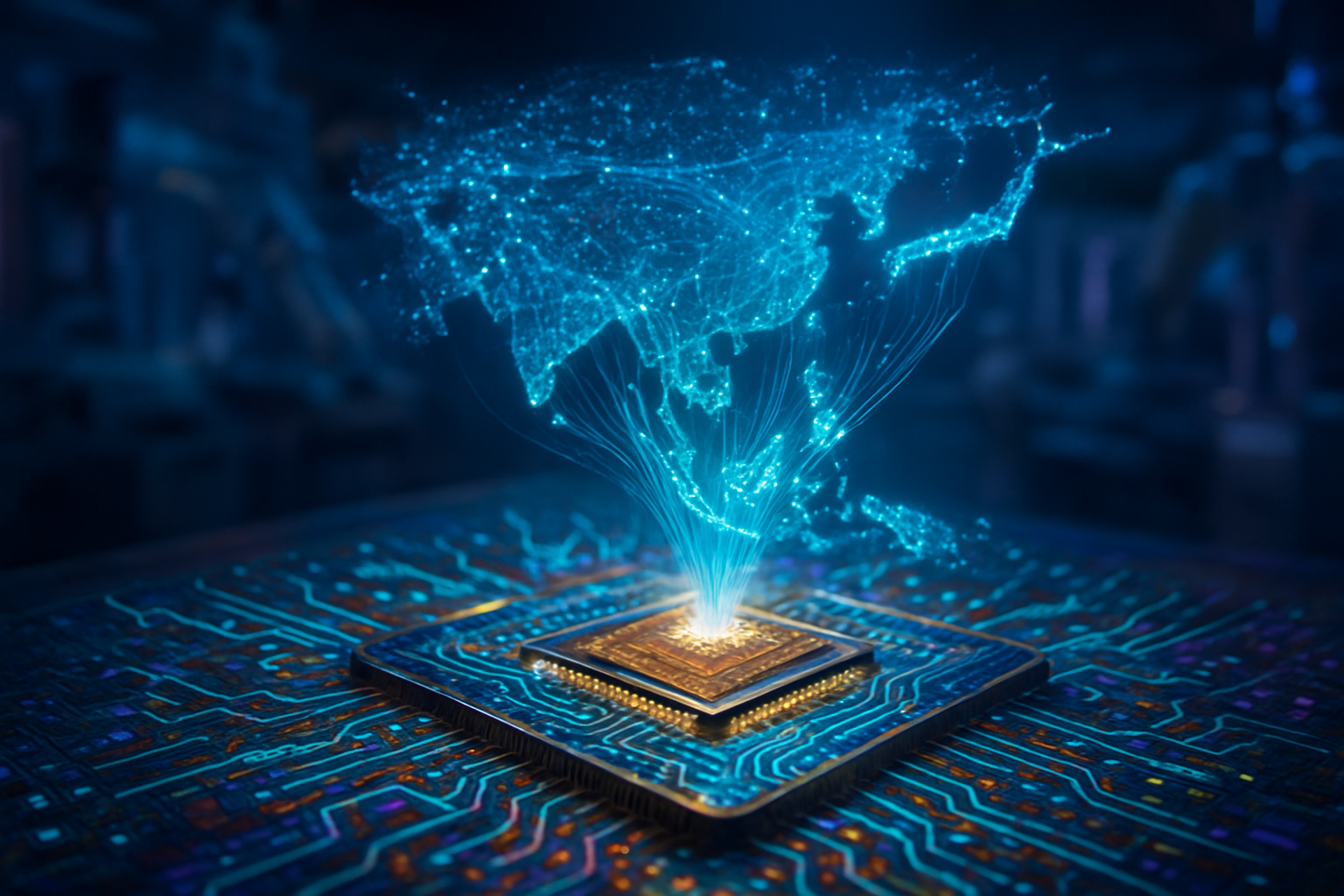
The $50 Billion Shift: Strategic Implications for Big Tech
The financial gravity of this trend was underscored by Broadcom’s recent revelation of an AI-specific backlog exceeding $73 billion, with annual custom silicon revenue projected to hit $50 billion by 2026. This is not just a rounding error; it represents a massive redirection of capital expenditure (CapEx) away from NVIDIA. For companies like Google and Microsoft, the move to custom silicon is a strategic necessity to protect their margins. As AI moves from the "R&D phase" to the "deployment phase," the cost of running inference for billions of users makes the $35,000+ price tag of a Blackwell GPU increasingly untenable.
The competitive implications are particularly stark for Broadcom, which has positioned itself as the "Kingmaker" of the custom silicon era. By providing the intellectual property and physical design services for chips like Google's TPU and Anthropic’s new $21 billion custom cluster, Broadcom is capturing the value that previously flowed almost exclusively to NVIDIA. This has created a bifurcated market: NVIDIA remains the essential partner for the most advanced "frontier" research—where the next generation of reasoning models is being birthed—while Broadcom and its partners are winning the war for "production-scale" AI.
For startups and smaller AI labs, this development is a double-edged sword. While the rise of custom silicon may eventually lower the cost of cloud compute, these bespoke chips are currently reserved for the "Big Five" hyperscalers. This creates a potential "compute divide," where the owners of custom silicon enjoy a significantly lower Total Cost of Ownership (TCO) than those relying on public cloud instances of NVIDIA GPUs. As a result, we are seeing a trend where major model builders, such as Anthropic, are seeking direct partnerships with silicon designers to secure their own long-term hardware independence.
A New Era of Efficiency: The Wider Significance of Custom Silicon
The rise of custom ASICs marks a pivotal transition in the AI landscape, mirroring the historical evolution of other computing paradigms. Just as the early days of the internet saw a transition from general-purpose CPUs to specialized networking hardware, the AI industry is realizing that the sheer energy demands of Blackwell-class clusters are unsustainable. In a world where data center power is the ultimate constraint, a 40% reduction in TCO and power consumption—offered by custom XPUs—is not just a financial preference; it is a requirement for continued scaling.
This shift also highlights the growing importance of the software compiler layer. One of NVIDIA’s strongest defenses has been CUDA, the software platform that has become the industry standard for AI development. However, the $50 billion investment in custom silicon is finally funding a viable alternative. Open-source initiatives like OpenAI’s Triton and Google’s OpenXLA are maturing, allowing developers to write code that can run on both NVIDIA GPUs and custom ASICs with minimal friction. As the software barrier to entry for custom silicon lowers, NVIDIA’s "software moat" begins to look less like a fortress and more like a hurdle.
There are, however, concerns regarding the fragmentation of the AI hardware ecosystem. If every major hyperscaler develops its own proprietary chip, the "write once, run anywhere" dream of AI development could become more difficult. We are seeing a divergence where the "Inference Era" is dominated by specialized, efficient hardware, while the "Innovation Era" remains tethered to the flexibility of NVIDIA. This could lead to a two-tier AI economy, where the most efficient models are those locked behind the proprietary hardware of a few dominant cloud providers.
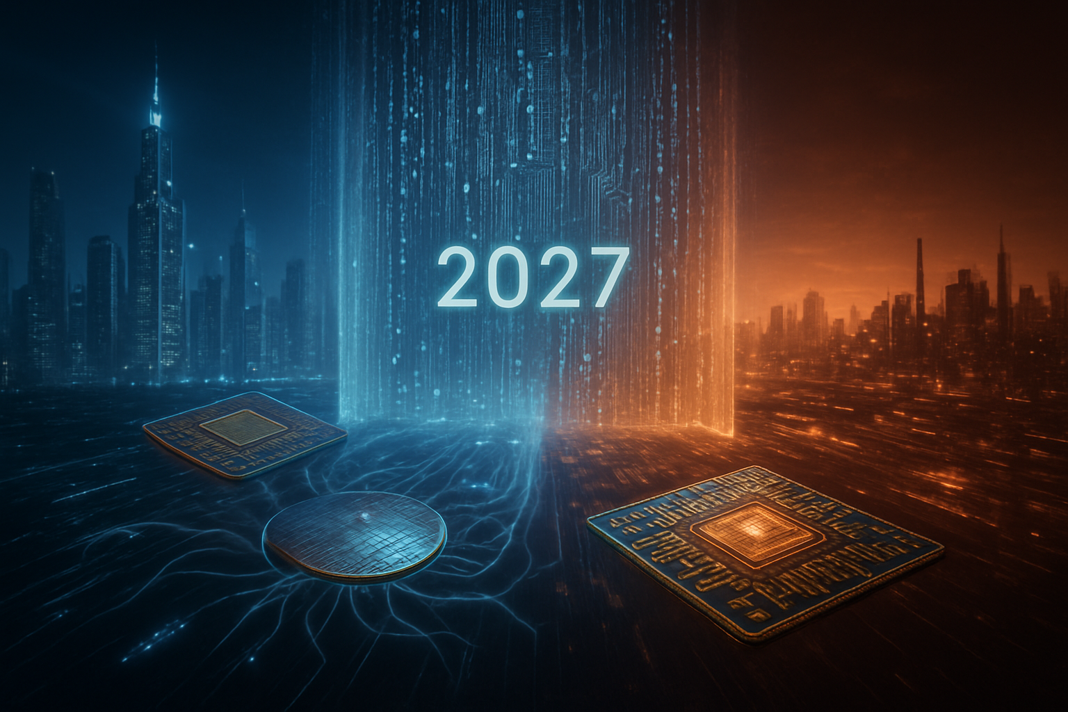
The Road to Rubin: Future Developments and the Next Frontier
Looking ahead to 2026, the battle is expected to intensify as NVIDIA prepares to launch its Rubin architecture (R100). Taped out on TSMC’s (NYSE: TSM) 3nm process, Rubin will feature HBM4 memory and a new 4x reticle chiplet design, aiming to reclaim the efficiency lead that custom ASICs have recently carved out. NVIDIA is also diversifying its own lineup, introducing "inference-first" GPUs like the Rubin CPX, which are designed to compete directly with custom XPUs on cost and power.
On the custom side, the next horizon is the "10-gigawatt chip" project. Reports suggest that major players like OpenAI are working with Broadcom on massive, multi-year silicon roadmaps that integrate power management and liquid cooling directly into the chip architecture. These "AI Super-ASICs" will be designed not just for today’s Transformers, but for the "test-time scaling" and agentic workflows that are expected to dominate the AI landscape in 2026 and beyond.
The ultimate challenge for both camps will be the physical limits of silicon. As we move toward 2nm and beyond, the gains from traditional Moore’s Law are diminishing. The next phase of competition will likely move beyond the chip itself and into the realm of "System-on-a-Wafer" and advanced 3D packaging. Experts predict that the winner of the next decade won't just be the company with the fastest chip, but the one that can most effectively manage the "Power-Performance-Area" (PPA) triad at a planetary scale.
Summary: The Bifurcation of AI Compute
The emergence of a $50 billion custom silicon market marks the end of the "GPU Monoculture." While NVIDIA’s Blackwell architecture remains a monumental achievement and the preferred tool for pushing the boundaries of what is possible, the economic and thermal realities of 2025 have forced a diversification of the hardware stack. Broadcom’s massive backlog and the aggressive chip roadmaps of Google, Microsoft, and Meta signal that the future of AI infrastructure is bespoke.
In the coming months, the industry will be watching the initial benchmarks of the Blackwell Ultra against the first wave of 3nm custom XPUs. If the efficiency gap continues to widen, NVIDIA may find itself in the position of a high-end boutique—essential for the most complex tasks but increasingly bypassed for the high-volume work that powers the global AI economy. For now, the silicon war is far from over, but the era of the universal GPU is clearly being challenged by a new generation of precision-engineered silicon.
This content is intended for informational purposes only and represents analysis of current AI developments.
TokenRing AI delivers enterprise-grade solutions for multi-agent AI workflow orchestration, AI-powered development tools, and seamless remote collaboration platforms.
For more information, visit https://www.tokenring.ai/.