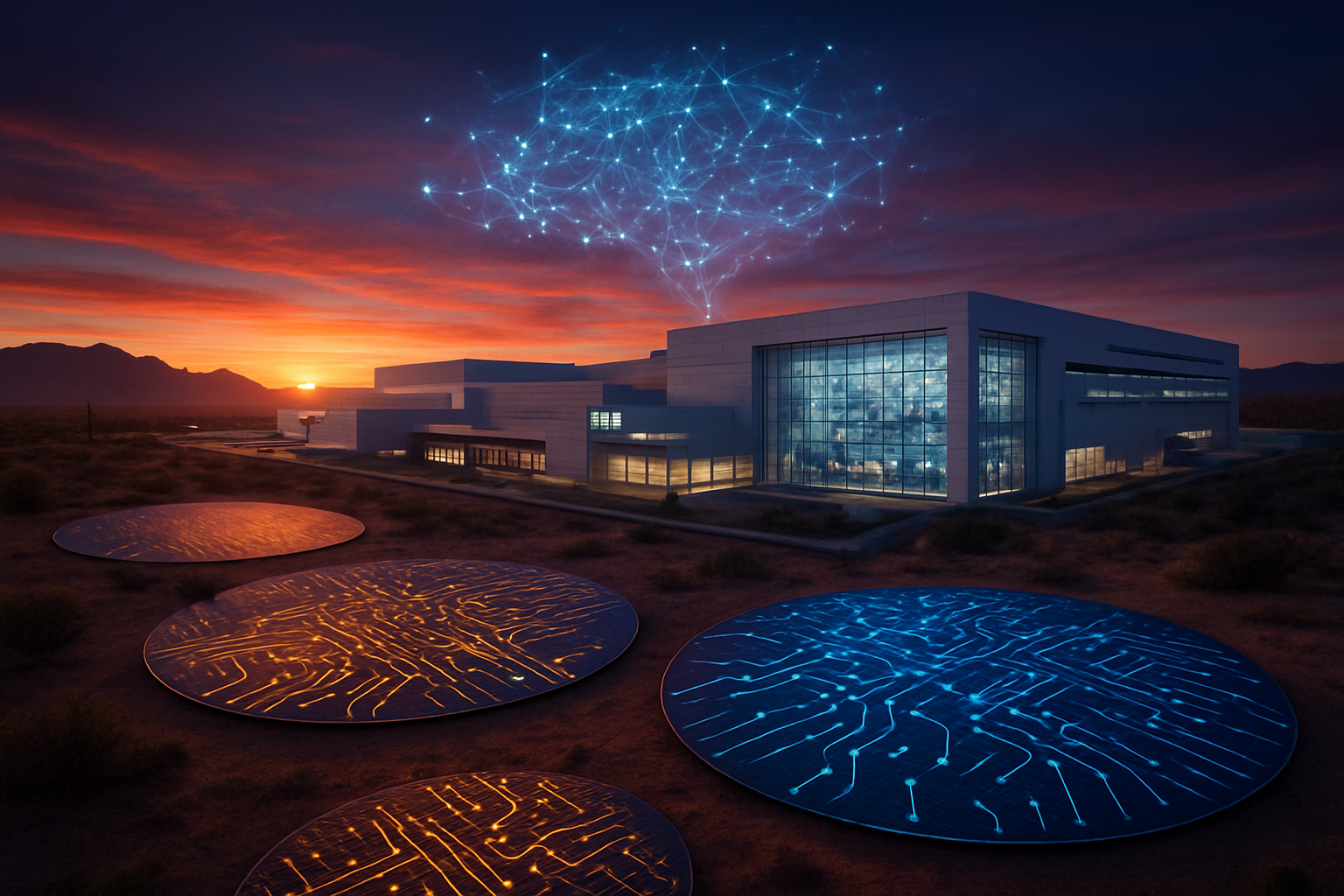
As of December 24, 2025, the desert landscape of Phoenix, Arizona, has officially transformed into a cornerstone of the global semiconductor industry. Taiwan Semiconductor Manufacturing Company (NYSE:TSM), the world’s leading foundry, has announced a series of milestones at its "Fab 21" site that have silenced critics and reshaped the geopolitical map of high-tech manufacturing. Most notably, the facility's Phase 1 has reached full volume production for 4nm and 5nm nodes, achieving a staggering 92% yield—a figure that remarkably surpasses the yields of TSMC’s comparable facilities in Taiwan by nearly 4%.
The immediate significance of this development cannot be overstated. For the first time, the United States is home to a facility capable of producing the world’s most advanced artificial intelligence and consumer electronics processors at a scale and efficiency that matches, or even exceeds, Asian counterparts. With the installation of 3nm equipment now underway and a clear roadmap toward 2nm volume production by late 2027, the "Arizona Gigafab" is no longer a theoretical project; it is an active, high-performance engine driving the next generation of AI innovation.
Technical Milestones: From 4nm Mastery to the 3nm Horizon
The technical achievements at Fab 21 represent a masterclass in technology transfer and precision engineering. Phase 1 is currently churning out 4nm (N4P) wafers for industry giants, utilizing advanced Extreme Ultraviolet (EUV) lithography to pack billions of transistors onto silicon. The reported 92% yield rate is a critical technical victory, proving that the highly complex chemical and mechanical processes required for sub-7nm manufacturing can be successfully replicated in the U.S. workforce environment. This success is attributed to a mix of automated precision systems and a rigorous training program that saw thousands of American engineers embedded in TSMC’s Tainan facilities over the past two years.
As Phase 1 reaches its stride, Phase 2 is entering the "cleanroom preparation" stage. This involves the installation of hyper-clean HVAC systems and specialized chemical delivery networks designed to support the 3nm (N3) process. Unlike the 5nm and 4nm nodes, the 3nm process offers a 15% speed improvement at the same power or a 30% power reduction at the same speed. The "tool-in" phase for the 3nm line, which includes the latest generation of EUV machines from ASML (NASDAQ:ASML), is slated for early 2026, with mass production pulled forward to 2027 due to overwhelming customer demand.
Looking further ahead, TSMC officially broke ground on Phase 3 in April 2025. This facility is being built specifically for the 2nm (N2) node, which will mark a historic transition from the traditional FinFET transistor architecture to Gate-All-Around (GAA) nanosheet technology. This architectural shift is essential for maintaining Moore’s Law, as it allows for better electrostatic control and lower leakage as transistors shrink to near-atomic scales. By the time Phase 3 is operational in late 2027, Arizona will be at the absolute bleeding edge of physics-defying semiconductor design.
The Power Players: Apple, Nvidia, and the localized Supply Chain
The primary beneficiaries of this expansion are the "Big Three" of the silicon world: Apple (NASDAQ:AAPL), NVIDIA (NASDAQ:NVDA), and AMD (NASDAQ:AMD). Apple has already secured the lion's share of Phase 1 capacity, using the Arizona-made 4nm chips for its latest A-series and M-series processors. For Apple, having a domestic source for its flagship silicon mitigates the risk of Pacific supply chain disruptions and aligns with its strategic goal of increasing U.S.-based manufacturing.
NVIDIA and AMD are equally invested, particularly as the demand for AI training hardware remains insatiable. NVIDIA’s Blackwell AI GPUs are now being fabricated in Phoenix, providing a critical buffer for the data center market. While silicon fabrication was the first step, a 2025 partnership with Amkor (NASDAQ:AMKR) has begun to localize advanced packaging services in Arizona as well. This means that for the first time, a chip can be designed, fabricated, and packaged within a 50-mile radius in the United States, drastically reducing the "wafer-to-market" timeline and strengthening the competitive advantage of American fabless companies.
This localized ecosystem creates a "virtuous cycle" for startups and smaller AI labs. As the heavyweights anchor the facility, the surrounding infrastructure—including specialized chemical suppliers and logistics providers—becomes more robust. This lowers the barrier to entry for smaller firms looking to secure domestic capacity for custom AI accelerators, potentially disrupting the current market where only the largest companies can afford the logistical hurdles of overseas manufacturing.
Geopolitics and the New Semiconductor Landscape
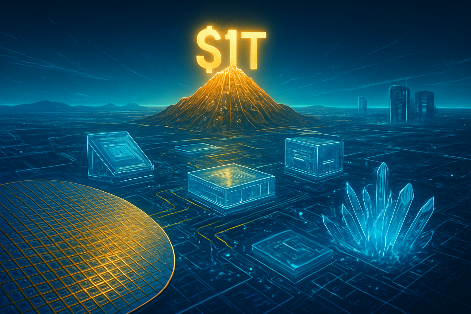
The progress in Arizona is a crowning achievement for the U.S. CHIPS and Science Act. The finalized agreement in late 2024, which provided TSMC with $6.6 billion in direct grants and $5 billion in loans, has proven to be a catalyst for broader investment. TSMC has since increased its total commitment to the Arizona site to a staggering $165 billion, planning a total of six fabs. This massive capital injection signals a shift in the global AI landscape, where "silicon sovereignty" is becoming as important as energy independence.
The success of the Arizona site also changes the narrative regarding the "Taiwan Risk." While Taiwan remains the undisputed heart of TSMC’s operations, the Arizona Gigafab provides a vital "hot spare" for the world’s most critical technology. Industry experts have noted that the 92% yield rate in Phoenix effectively debunked the myth that high-end semiconductor manufacturing is culturally or geographically tethered to East Asia. This milestone serves as a blueprint for other nations—such as Germany and Japan—where TSMC is also expanding, suggesting a more decentralized and resilient global chip supply.
However, this expansion is not without its concerns. The sheer scale of the Phoenix operations has placed immense pressure on local water resources and the energy grid. While TSMC has implemented world-leading water reclamation technologies, the environmental impact of a six-fab complex in a desert remains a point of contention and a challenge for local policymakers. Furthermore, the "N-2" policy—where Taiwan-based fabs must remain two generations ahead of overseas sites—ensures that while Arizona is cutting-edge, the absolute pinnacle of research and development remains in Hsinchu.
The Road to 2027: 2nm and the A16 Node
The roadmap for the next 24 months is clear but ambitious. Following the 3nm equipment installation in 2026, the industry will be watching for the first "pilot runs" of 2nm silicon in late 2027. The 2nm node is expected to be the workhorse for the next generation of AI models, providing the efficiency needed for edge-AI devices—like glasses and wearables—to perform complex reasoning without tethering to the cloud.
Beyond 2nm, TSMC has already hinted at the "A16" node (1.6nm), which will introduce backside power delivery. This technology moves the power wiring to the back of the wafer, freeing up space on the front for more signal routing and denser transistor placement. Experts predict that if the current construction pace holds, Arizona could see A16 production as early as 2028 or 2029, effectively turning the desert into the most advanced square mile of real estate on the planet.
The primary challenge moving forward will be the talent pipeline. While the yield rates are high, the demand for specialized technicians and EUV operators is expected to triple as Phase 2 and Phase 3 come online. TSMC, along with partners like Intel (NASDAQ:INTC), which is also expanding in Arizona, will need to continue investing heavily in local university programs and vocational training to sustain this growth.
A New Era for American Silicon
TSMC’s progress in Arizona marks a definitive turning point in the history of technology. The transition from a construction site to a high-yield, high-volume 4nm manufacturing hub—with 3nm and 2nm nodes on the immediate horizon—represents the successful "re-shoring" of the world’s most complex industrial process. It is a validation of the CHIPS Act and a testament to the collaborative potential of global tech leaders.
As we look toward 2026, the focus will shift from "can they build it?" to "how fast can they scale it?" The installation of 3nm equipment in the coming months will be the next major benchmark to watch. For the AI industry, this means more chips, higher efficiency, and a more secure supply chain. For the world, it means that the brains of our most advanced machines are now being forged in the heart of the American Southwest.
This content is intended for informational purposes only and represents analysis of current AI developments.
TokenRing AI delivers enterprise-grade solutions for multi-agent AI workflow orchestration, AI-powered development tools, and seamless remote collaboration platforms.
For more information, visit https://www.tokenring.ai/.