As artificial intelligence models swell toward the 100-trillion-parameter mark, the industry has hit a physical wall: the "data traffic jam." Traditional copper-based networking and even standard optical transceivers are struggling to keep pace with the massive throughput required to synchronize thousands of GPUs in real-time. To solve this, the tech industry is undergoing a fundamental shift, moving from electrical signals to light-speed data transfer through the integration of silicon photonics directly onto silicon wafers.
The emergence of silicon photonics marks a pivotal moment in the evolution of the "AI Factory." By embedding lasers and optical components into the same packages as processors and switches, companies are effectively removing the bottlenecks that have long plagued high-performance computing (HPC). Leading this charge is NVIDIA (NASDAQ: NVDA) with its Spectrum-X platform, which is redefining how data moves across the world’s most powerful AI clusters, enabling the next generation of generative AI models to train faster and more efficiently than ever before.
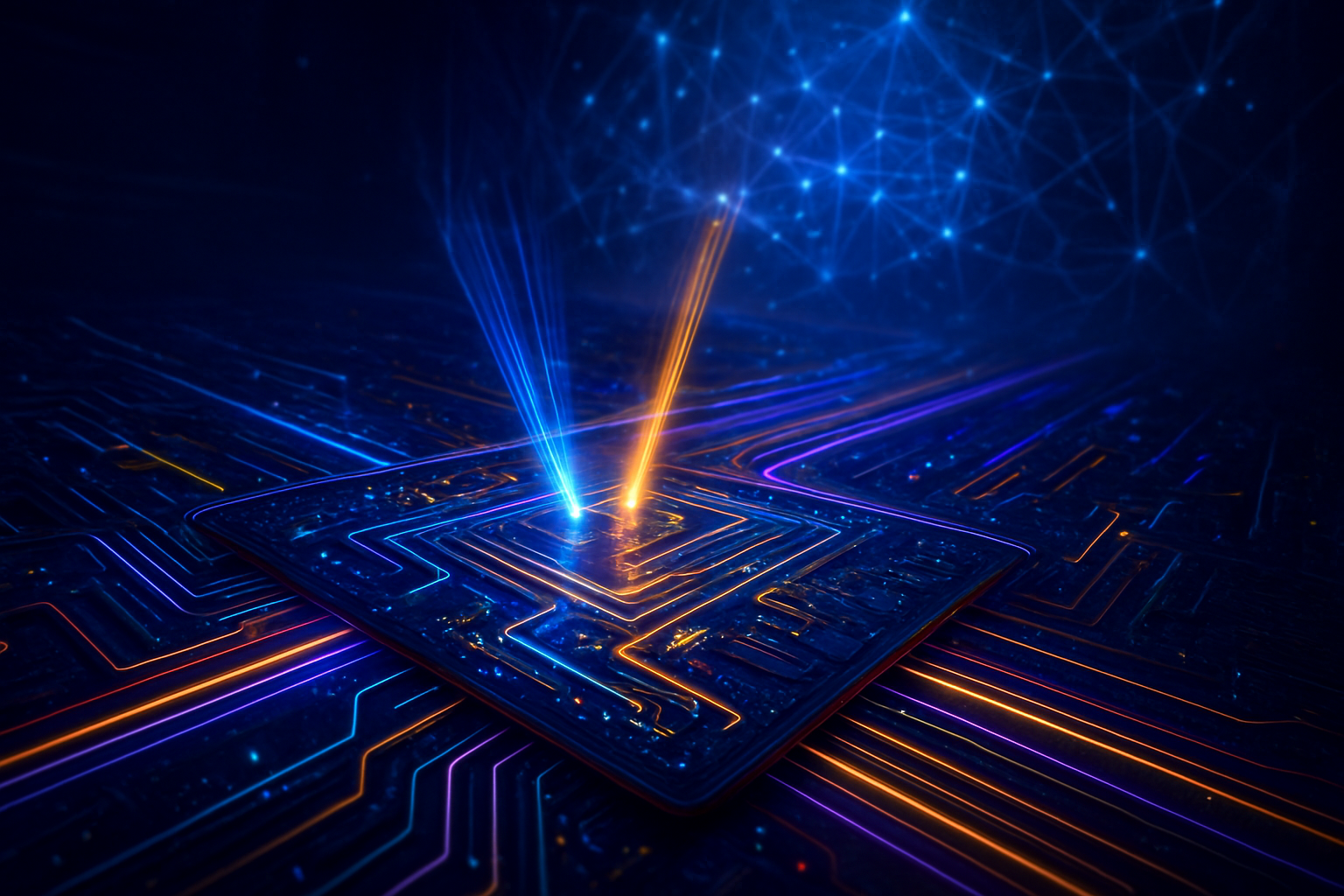
The Light-Speed Revolution: Integrating Lasers on Silicon
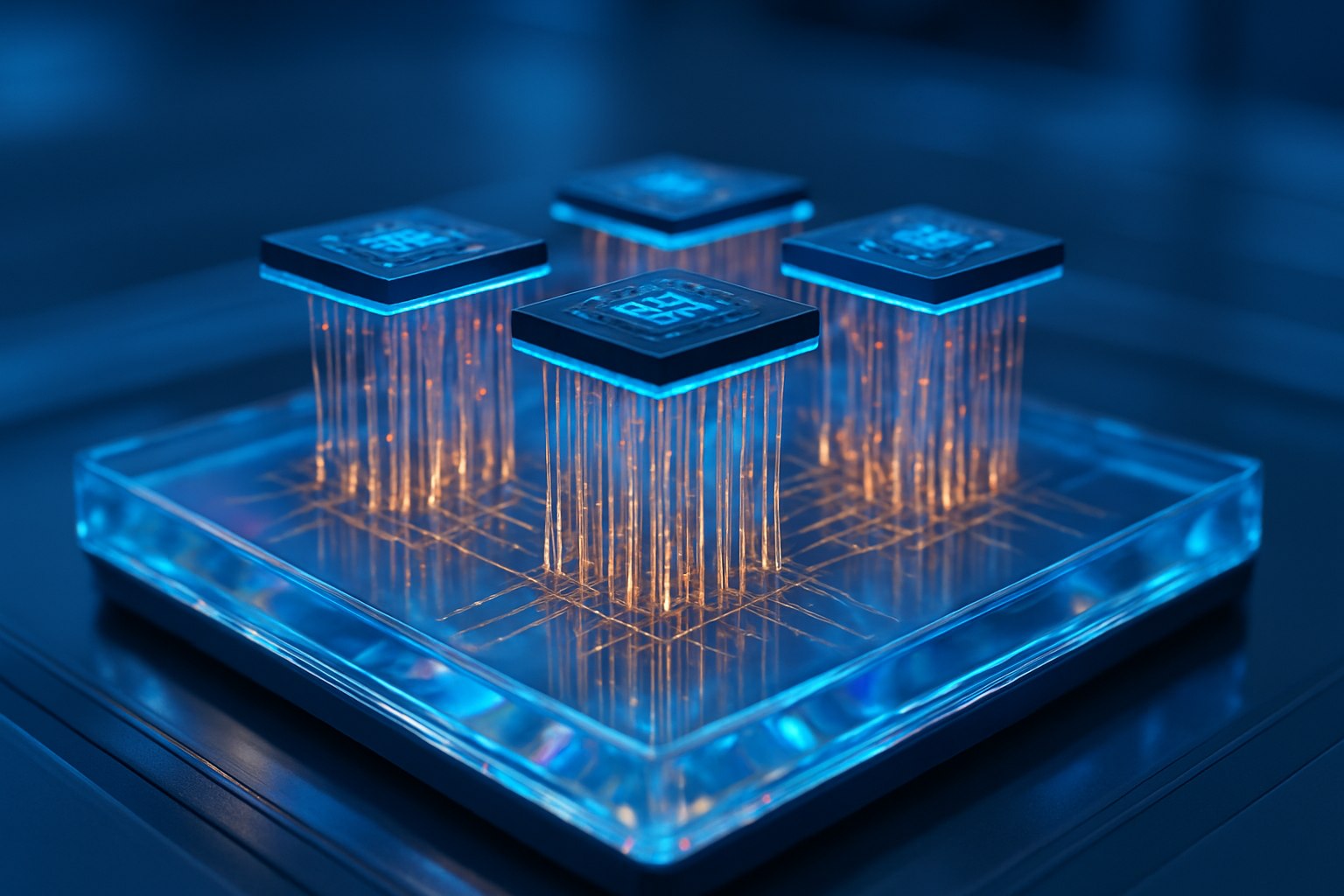
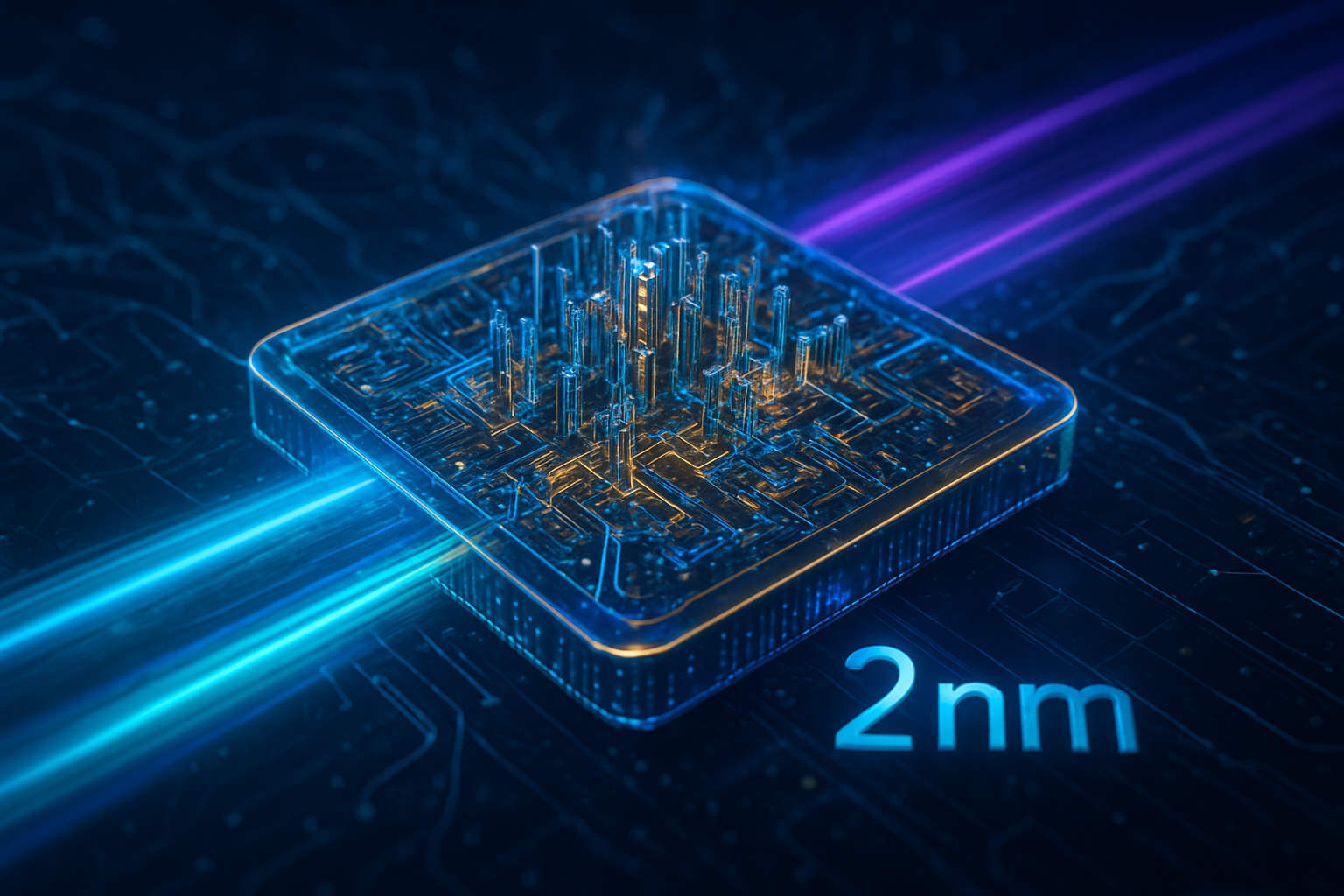
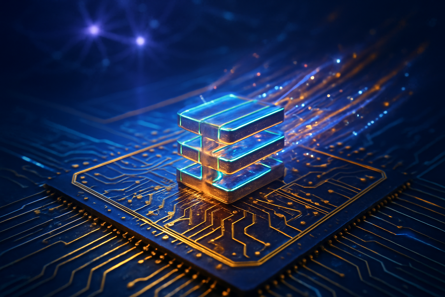
The technical breakthrough at the heart of this transition is the successful integration of lasers directly onto silicon wafers—a feat once considered the "Holy Grail" of semiconductor engineering. Historically, silicon is a poor emitter of light, necessitating external laser sources and bulky pluggable transceivers. However, by late 2025, heterogeneous integration—the process of bonding light-emitting materials like Indium Phosphide onto 300mm silicon wafers—has become a commercially viable reality. This allows for Co-Packaged Optics (CPO), where the optical engine sits in the same package as the switch silicon, drastically reducing the distance data must travel via electricity.
NVIDIA’s Spectrum-X Ethernet Photonics platform is a prime example of this advancement. Unveiled as a cornerstone of the Blackwell-era networking stack, Spectrum-X now supports staggering switch throughputs of up to 400 Tbps in high-density configurations. By utilizing TSMC’s Compact Universal Photonic Engine (COUPE) technology, NVIDIA has 3D-stacked electronic and photonic circuits, eliminating the need for power-hungry Digital Signal Processors (DSPs). This architecture supports 1.6 Tbps per port, providing the massive bandwidth density required to feed trillion-parameter models without the latency spikes that typically derail large-scale training jobs.
The shift to silicon photonics isn't just about speed; it's about resiliency. In traditional setups, "link flaps"—brief interruptions in data flow—are a common occurrence that can crash a training session involving 100,000 GPUs. Industry data suggests that silicon photonics-based networking, such as NVIDIA’s Quantum-X Photonics, offers up to 10x higher resiliency. This allows trillion-parameter model training to run for weeks without interruption, a necessity when the cost of a single training run can reach hundreds of millions of dollars.
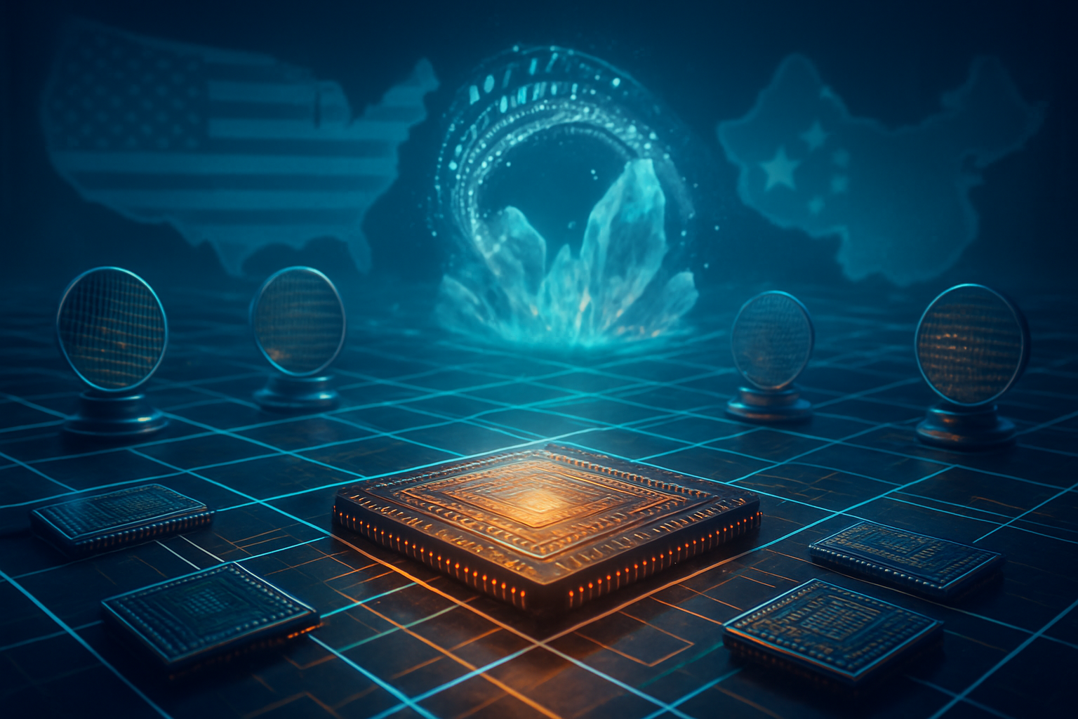
The Strategic Battle for the AI Backbone
The move to silicon photonics has ignited a fierce competitive landscape among semiconductor giants and specialized startups. While NVIDIA (NASDAQ: NVDA) currently dominates the GPU-to-GPU interconnect market, Intel (NASDAQ: INTC) has positioned itself as a volume leader in integrated photonics. Having shipped over 32 million integrated lasers by the end of 2025, Intel is leveraging its "Optical Compute Interconnect" (OCI) chiplets to bridge the gap between CPUs, GPUs, and high-bandwidth memory, potentially challenging NVIDIA’s full-stack dominance in the data center.
Broadcom (NASDAQ: AVGO) has also emerged as a heavyweight in this arena with its "Bailly" CPO switch series. By focusing on open standards and high-volume manufacturing, Broadcom is targeting hyperscalers who want to build massive AI clusters without being locked into a single vendor's ecosystem. Meanwhile, startups like Ayar Labs are playing a critical role; their TeraPHY™ optical I/O chiplets, which achieved 8 Tbps of bandwidth in recent 2025 trials, are being integrated by multiple partners to provide the high-speed "on-ramps" for optical data.
This shift is disrupting the traditional transceiver market. Companies that once specialized in pluggable optical modules are finding themselves forced to pivot or partner with silicon foundries to stay relevant. For AI labs and tech giants, the strategic advantage now lies in who can most efficiently manage the "power-per-bit" ratio. Those who successfully implement silicon photonics can build larger clusters within the same power envelope, a critical factor as data centers begin to consume a double-digit percentage of the global energy supply.
Scaling the Unscalable: Efficiency and the Future of AI Factories
The broader significance of silicon photonics extends beyond raw performance; it is an environmental and economic necessity. As AI clusters scale toward millions of GPUs, the power consumption of traditional networking becomes unsustainable. Silicon photonics delivers approximately 3.5x better power efficiency compared to traditional pluggable transceivers. In a 400,000-GPU "AI Factory," switching to integrated optics can save tens of megawatts of power—enough to power a small city—while reducing total cluster power consumption by as much as 12%.
This development fits into the larger trend of "computational convergence," where the network itself becomes part of the computer. With protocols like SHARPv4 (Scalable Hierarchical Aggregation and Reduction Protocol) integrated into photonic switches, the network can perform mathematical operations on data while it is in transit. This "in-network computing" offloads tasks from the GPUs, accelerating the convergence of 100-trillion-parameter models and reducing the overall time-to-solution.
However, the transition is not without concerns. The complexity of 3D-stacking photonics and electronics introduces new challenges in thermal management and manufacturing yield. Furthermore, the industry is still debating the standards for optical interconnects, with various proprietary solutions competing for dominance. Comparisons are already being made to the transition from copper to fiber optics in the telecommunications industry decades ago—a shift that took years to fully mature but eventually became the foundation of the modern internet.
Beyond the Rack: The Road to Optical Computing
Looking ahead, the roadmap for silicon photonics suggests that we are only at the beginning of an "optical era." In the near term (2026-2027), we expect to see the first widespread deployments of 3.2 Tbps per port networking and the integration of optical I/O directly into the GPU die. This will effectively turn the entire data center into a single, massive "super-node," where the distance between two chips no longer dictates the speed of their communication.
Potential applications extend into the realm of edge AI and autonomous systems, where low-latency, high-bandwidth communication is vital. Experts predict that as the cost of silicon photonics drops due to economies of scale, we may see optical interconnects appearing in consumer-grade hardware, enabling ultra-fast links between PCs and external AI accelerators. The ultimate goal remains "optical computing," where light is used not just to move data, but to perform the calculations themselves, potentially offering a thousand-fold increase in efficiency over electronic transistors.
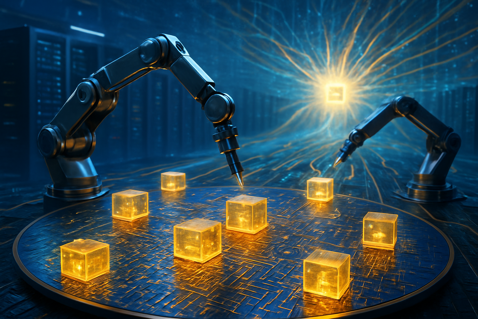
The immediate challenge remains the high-volume manufacturing of integrated lasers. While Intel and TSMC have made significant strides, achieving the yields necessary for global scale remains a hurdle. As the industry moves toward 200G-per-lane architectures, the precision required for optical alignment will push the boundaries of robotic assembly and semiconductor lithography.
A New Era for AI Infrastructure
The integration of silicon photonics into the AI stack represents one of the most significant infrastructure shifts in the history of computing. By moving data at the speed of light and integrating lasers directly onto silicon, the industry is effectively bypassing the physical limits of electricity. NVIDIA’s Spectrum-X and the innovations from Intel and Broadcom are not just incremental upgrades; they are the foundational technologies that will allow AI to scale to the next level of intelligence.
The key takeaway for the industry is that the "data traffic jam" is finally clearing. As we move into 2026, the focus will shift from how many GPUs a company can buy to how efficiently they can connect them. Silicon photonics has become the prerequisite for any organization serious about training the 100-trillion-parameter models of the future.
In the coming weeks and months, watch for announcements regarding the first live deployments of 1.6T CPO switches in hyperscale data centers. These early adopters will likely set the pace for the next wave of AI breakthroughs, proving that in the race for artificial intelligence, speed—quite literally—is everything.
This content is intended for informational purposes only and represents analysis of current AI developments.
TokenRing AI delivers enterprise-grade solutions for multi-agent AI workflow orchestration, AI-powered development tools, and seamless remote collaboration platforms.
For more information, visit https://www.tokenring.ai/.