Tag: Semiconductors

  • The Silicon Frontier: TSMC’s A16 and Super Power Rail Redefine the AI Chip Race

    The Silicon Frontier: TSMC’s A16 and Super Power Rail Redefine the AI Chip Race

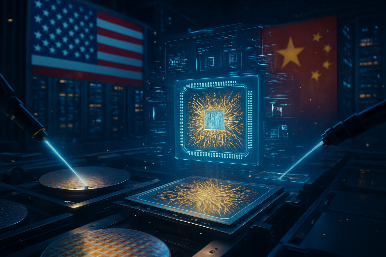
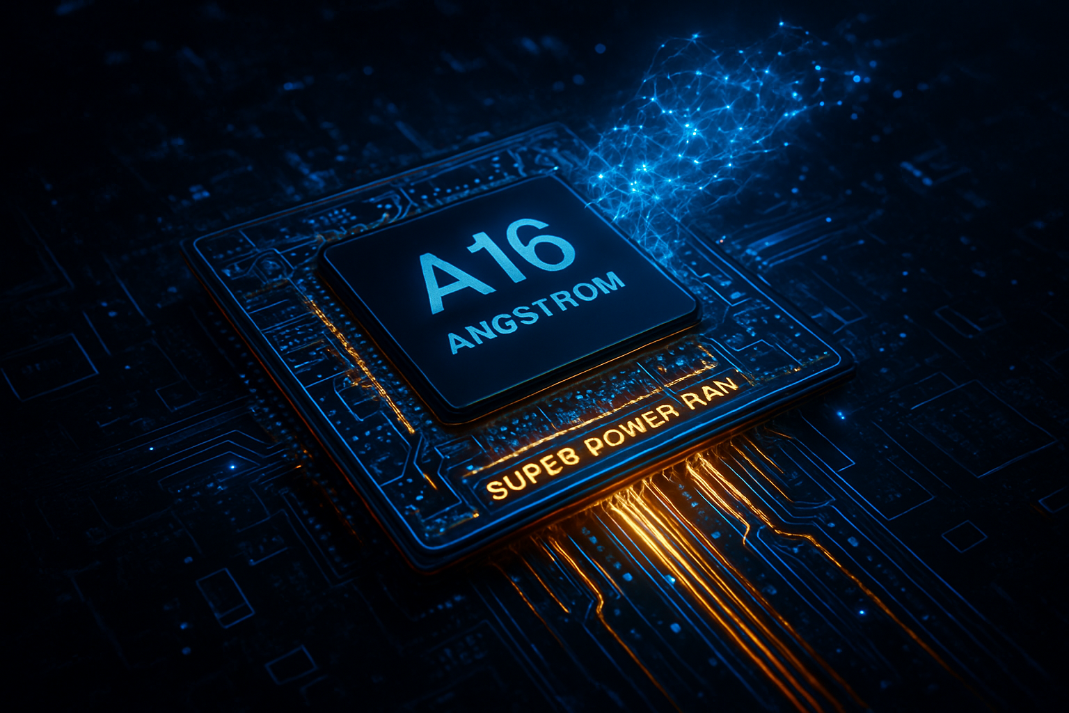
    As the global appetite for artificial intelligence continues to outpace existing hardware capabilities, the semiconductor industry has reached a historic inflection point. Taiwan Semiconductor Manufacturing Company (NYSE: TSM), the world’s largest contract chipmaker, has officially entered the "Angstrom Era" with the unveiling of its A16 process. This 1.6nm-class node represents more than just a reduction in transistor size; it introduces a fundamental architectural shift known as "Super Power Rail" (SPR). This breakthrough is designed to solve the physical bottlenecks that have long plagued high-performance computing, specifically the routing congestion and power delivery issues that limit the scaling of next-generation AI accelerators.

    The significance of A16 cannot be overstated. For the first time in decades, the primary driver for leading-edge process nodes has shifted from mobile devices to AI data centers. While Apple Inc. (NASDAQ: AAPL) has traditionally been the first to adopt TSMC’s newest technologies, the A16 node is being tailor-made for the massive, power-hungry GPUs and custom ASICs that fuel Large Language Models (LLMs). By moving the power delivery network to the backside of the wafer, TSMC is effectively doubling the available space for signal routing, enabling a leap in performance and energy efficiency that was previously thought to be hitting a physical wall.

    The Architecture of Angstrom: Nanosheets and Super Power Rails

    Technically, the A16 process is an evolution of TSMC’s 2nm (N2) family, utilizing second-generation Gate-All-Around (GAA) Nanosheet transistors. However, the true innovation lies in the Super Power Rail (SPR), TSMC’s proprietary implementation of Backside Power Delivery (BSPDN). In traditional chip manufacturing, both signal wires and power lines are crammed onto the front side of the silicon wafer. As transistors shrink, these wires compete for space, leading to "routing congestion" and significant "IR drop"—a phenomenon where voltage decreases as it travels through the complex web of circuitry. SPR solves this by moving the entire power delivery network to the backside of the wafer, allowing the front side to be dedicated exclusively to signal routing.

    Unlike the "PowerVia" approach currently being deployed by Intel Corporation (NASDAQ: INTC), which uses nano-Through Silicon Vias (nTSVs) to bridge the power network to the transistors, TSMC’s Super Power Rail connects the power network directly to the transistor’s source and drain. This direct-contact scheme is significantly more complex to manufacture but offers superior electrical characteristics. According to TSMC, A16 provides an 8% to 10% speed boost at the same voltage compared to its N2P process, or a 15% to 20% reduction in power consumption at the same clock speed. Furthermore, the removal of power rails from the front side allows for a logic density improvement of up to 1.1x, enabling more transistors to be packed into the same physical area.

    Initial reactions from the AI research community and industry experts have been overwhelmingly positive, though cautious regarding the manufacturing complexity. Dr. Wei-Chung Hsu, a senior semiconductor analyst, noted that "A16 is the most aggressive architectural change we’ve seen since the transition to FinFET. By decoupling power and signal, TSMC is giving chip designers a clean slate to optimize for the 1000-watt chips that the AI era demands." This sentiment is echoed by EDA (Electronic Design Automation) partners who are already racing to update their software tools to handle the unique thermal and routing challenges of backside power.

    The AI Power Play: NVIDIA and OpenAI Take the Lead

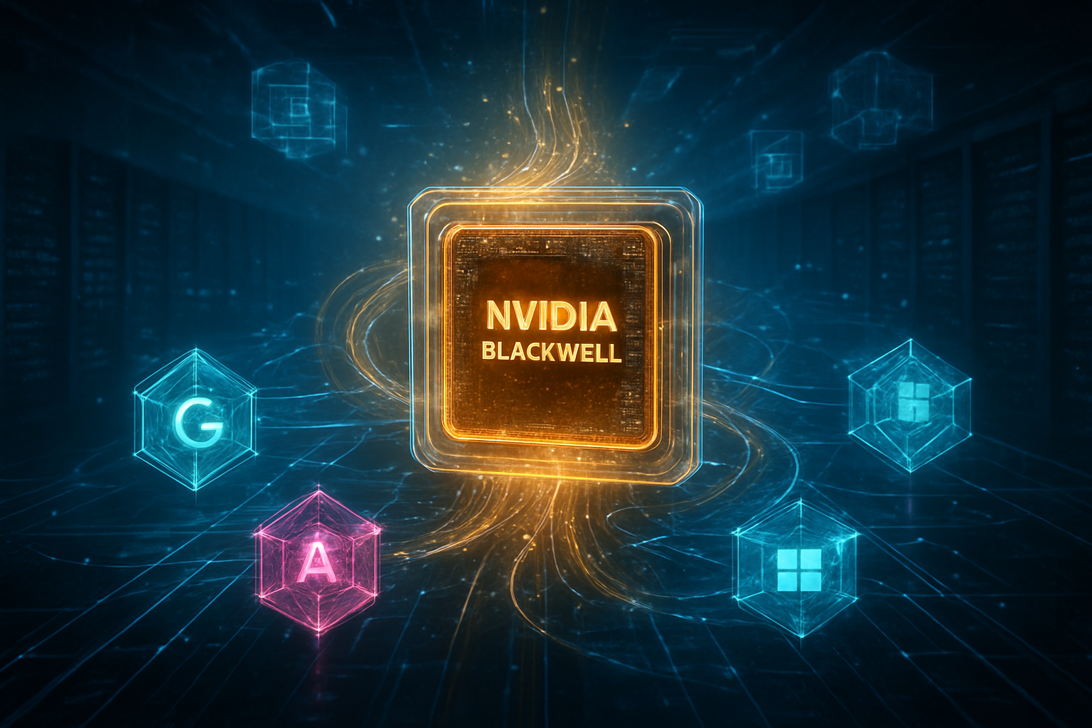
    The shift to A16 has triggered a massive realignment among tech giants. For the first decade of the smartphone era, Apple was the undisputed "anchor tenant" for every new TSMC node. However, as of late 2025, reports indicate that NVIDIA Corporation (NASDAQ: NVDA) has secured the lion's share of A16 capacity for its upcoming "Feynman" architecture GPUs, expected to arrive in 2027. These chips will be the first to leverage Super Power Rail to manage the extreme power densities required for trillion-parameter model training.

    Furthermore, the A16 era marks the entry of new players into the leading-edge foundry market. OpenAI is reportedly working with Broadcom Inc. (NASDAQ: AVGO) to design its first in-house AI inference chips on the A16 node, aiming to reduce its multi-billion dollar reliance on external hardware vendors. This move positions OpenAI not just as a software leader, but as a vertical integrator capable of competing with established silicon incumbents. Meanwhile, Advanced Micro Devices (NASDAQ: AMD) is expected to follow suit, utilizing A16 for its MI400 series to maintain parity with NVIDIA’s performance gains.

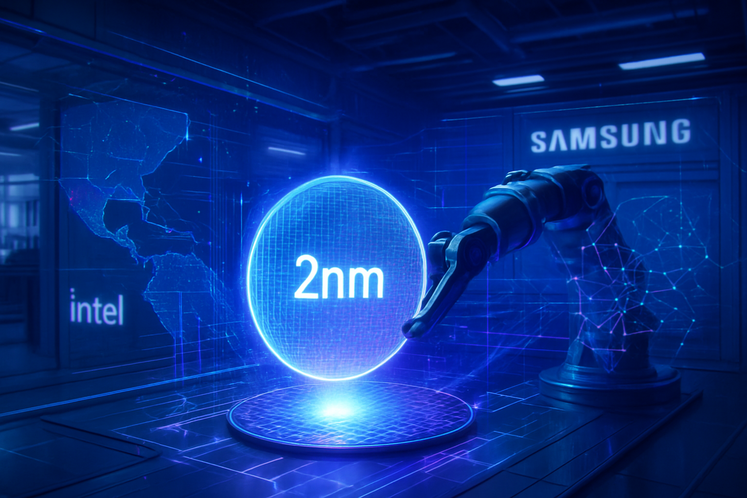
    Intel, however, remains a formidable challenger. While Samsung Electronics (KRX: 005930) has reportedly delayed its 1.4nm mass production to 2029 due to yield issues, Intel’s 14A node is on track for 2026/2027. Intel is betting heavily on ASML’s (NASDAQ: ASML) High-NA EUV lithography—a technology TSMC has notably deferred for the A16 node in favor of more mature, cost-effective standard EUV. This creates a fascinating strategic divergence: TSMC is prioritizing architectural innovation (SPR), while Intel is prioritizing lithographic precision. For AI startups and cloud providers, this competition is a boon, offering two distinct paths to sub-2nm performance and a much-needed diversification of the global supply chain.

    Beyond Moore’s Law: The Broader Implications for AI Infrastructure

    The arrival of A16 and backside power delivery is more than a technical milestone; it is a necessity for the survival of the AI boom. Current AI data centers are facing a "power wall," where the energy required to cool and power massive GPU clusters is becoming the primary constraint on growth. By delivering a 20% reduction in power consumption, A16 allows data center operators to either reduce their carbon footprint or, more likely, pack 20% more compute power into the same energy envelope. This efficiency is critical as the industry moves toward "sovereign AI," where nations seek to build their own localized data centers to protect data privacy.

    However, the transition to A16 is not without its concerns. The cost of manufacturing these "Angstrom-class" wafers is skyrocketing, with industry estimates placing the price of a single A16 wafer at nearly $50,000. This represents a significant jump from the $20,000 price point seen during the 5nm era. Such high costs could lead to a bifurcation of the tech industry, where only the wealthiest "hyperscalers" like Microsoft (NASDAQ: MSFT), Alphabet (NASDAQ: GOOGL), and Amazon (NASDAQ: AMZN) can afford the absolute cutting edge, potentially widening the gap between AI leaders and smaller startups.

    Thermal management also presents a new set of challenges. With the power delivery network moved to the back of the chip, "hot spots" are now buried under layers of metal, making traditional top-side cooling less effective. This is expected to accelerate the adoption of liquid cooling and immersion cooling technologies in AI data centers, as traditional air cooling reaches its physical limits. The A16 node is thus acting as a catalyst for innovation across the entire data center stack, from the transistor level up to the facility's cooling infrastructure.

    The Roadmap Ahead: From 1.6nm to 1.4nm and Beyond

    Looking toward the future, TSMC’s A16 is just the beginning of a rapid-fire roadmap. Risk production is scheduled to begin in early 2026, with volume production ramping up in the second half of the year. This puts the first A16-powered AI chips on the market by early 2027. Following closely behind is the A14 (1.4nm) node, which will likely integrate the High-NA EUV machines that TSMC is currently evaluating in its research labs. This progression suggests that the cadence of semiconductor innovation has actually accelerated in response to the AI gold rush, defying predictions that Moore’s Law was nearing its end.

    Near-term developments will likely focus on "3D IC" packaging, where A16 logic chips are stacked directly on top of HBM4 (High Bandwidth Memory) or other logic dies. This "System-on-Integrated-Chips" (SoIC) approach will be necessary to keep the data flowing fast enough to satisfy A16’s increased processing power. Experts predict that the next two years will see a flurry of announcements regarding "chiplet" ecosystems, as designers mix and match A16 high-performance cores with older, cheaper nodes for less critical functions to manage the soaring costs of 1.6nm silicon.

    A New Era of Compute

    TSMC’s A16 process and the introduction of Super Power Rail represent a masterful response to the unique demands of the AI era. By moving power delivery to the backside of the wafer, TSMC has bypassed the routing bottlenecks that threatened to stall chip performance, providing a clear path to 1.6nm and beyond. The shift in lead customers from mobile to AI underscores the changing priorities of the global economy, as the race for compute power becomes the defining competition of the 21st century.

    As we look toward 2026 and 2027, the industry will be watching two things: the yield rates of TSMC’s SPR implementation and the success of Intel’s High-NA EUV strategy. The duopoly between TSMC and Intel at the leading edge will provide the foundation for the next generation of AI breakthroughs, from real-time video generation to autonomous scientific discovery. While the costs are higher than ever, the potential rewards of Angstrom-class silicon ensure that the silicon frontier will remain the most watched space in technology for years to come.


    This content is intended for informational purposes only and represents analysis of current AI developments.

    TokenRing AI delivers enterprise-grade solutions for multi-agent AI workflow orchestration, AI-powered development tools, and seamless remote collaboration platforms.
    For more information, visit https://www.tokenring.ai/.

  • India’s Semiconductor Rise: The Rohm and Tata Partnership

    India’s Semiconductor Rise: The Rohm and Tata Partnership

    In a landmark move that cements India’s position as a burgeoning titan in the global technology supply chain, Rohm Co., Ltd. (TYO: 6963) and Tata Electronics have officially entered into a strategic partnership to establish a domestic semiconductor manufacturing ecosystem. Announced on December 22, 2025, this collaboration focuses on the high-growth sector of power semiconductors—the essential hardware that manages electricity in everything from electric vehicle (EV) drivetrains to the massive data centers powering modern artificial intelligence.

    The partnership represents a critical milestone for the India Semiconductor Mission (ISM), a $10 billion government initiative designed to reduce reliance on foreign imports and build a "China Plus One" alternative for global electronics. By combining Rohm’s decades of expertise in Integrated Device Manufacturing (IDM) with the industrial scale of the Tata Group, the two companies aim to localize the entire value chain—from design and wafer fabrication to advanced packaging and testing—positioning India as a primary node in the global chip architecture.

    Powering the Future: Technical Specifications and the Shift to Wide-Bandgap Materials

    The technical core of the Rohm-Tata partnership centers on the production of advanced power semiconductors, which are significantly more complex to manufacture than standard logic chips. The first product slated for production is an India-designed, automotive-grade N-channel 100V, 300A Silicon MOSFET. This device utilizes a TOLL (Transistor Outline Leadless) package, a specialized form factor that offers superior thermal management and high current density, making it ideal for the demanding power-switching requirements of modern electric drivetrains and industrial automation.

    Beyond traditional silicon, the collaboration is heavily focused on "wide-bandgap" (WBG) materials, specifically Silicon Carbide (SiC) and Gallium Nitride (GaN). Rohm is a recognized global leader in SiC technology, which allows for higher voltage operation and significantly faster switching speeds than traditional silicon. In practical terms, SiC modules can reduce switching losses by up to 85%, a technical leap that is essential for extending the range of EVs and shrinking the footprint of the power inverters used in AI-driven smart grids.

    This approach differs from previous attempts at Indian semiconductor manufacturing by focusing on "specialty" chips rather than just chasing the smallest nanometer nodes. While the industry often focuses on 3nm or 5nm logic chips for CPUs, the power semiconductors being developed by Rohm and Tata are the "muscles" of the digital world. Industry experts note that by securing the supply of these specialized components, India is addressing a critical bottleneck in the global supply chain that was exposed during the shortages of 2021-2022.

    Market Disruption: Tata’s Manufacturing Might Meets Rohm’s Design Prowess

    The strategic implications of this deal for the global market are profound. Tata Electronics, a subsidiary of the storied Tata Group, is leveraging its massive new facilities in Jagiroad, Assam, and Dholera, Gujarat, to provide the backend infrastructure. The Jagiroad Assembly and Test (ATMP) facility, a $3.2 billion investment, has already begun commissioning and is expected to handle the bulk of the Rohm-designed chip packaging. This allows Rohm to scale its production capacity without the massive capital expenditure of building new wholly-owned fabs in Japan or Malaysia.

    For the broader tech ecosystem, the partnership creates a formidable competitor to established players in the power semi space like Infineon and STMicroelectronics. Companies within the Tata umbrella, such as Tata Motors (NSE: TATAMOTORS) and Tata Elxsi (NSE: TATAELXSI), stand to benefit immediately from a localized, secure supply of high-efficiency chips. This vertical integration provides a significant strategic advantage, insulating the Indian automotive and aerospace sectors from geopolitical volatility in the Taiwan Strait or the South China Sea.

    Furthermore, the "Designed in India, Manufactured in India" nature of this partnership qualifies it for the highest tier of government incentives. Under the ISM, the project receives nearly 50% fiscal support for capital expenditure, a level of subsidy that makes the Indian-produced chips highly competitive on the global export market. This cost advantage, combined with Rohm’s reputation for reliability, is expected to attract major global OEMs looking to diversify their supply chains away from East Asian hubs.

    The Geopolitical Shift: India as a Global Semiconductor Hub

    The Rohm-Tata partnership is more than just a corporate deal; it is a manifestation of the "China Plus One" strategy that is reshaping global geopolitics. As the United States and its allies continue to restrict the flow of advanced AI hardware to certain regions, India is positioning itself as a neutral, democratic alternative for high-tech manufacturing. This development fits into a broader trend where India is no longer just a consumer of technology but a critical architect of the hardware that runs it.

    This shift has massive implications for the AI landscape. While much of the public discourse around AI focuses on Large Language Models (LLMs), the physical infrastructure—the data centers and cooling systems—requires sophisticated power management. The SiC and GaN chips produced by this partnership are the very components that make "Green AI" possible by reducing the energy footprint of massive server farms. By localizing this production, India is ensuring that its own AI ambitions are supported by a resilient and efficient hardware foundation.

    The significance of this milestone can be compared to the early days of the IT services boom in India, but with a much higher barrier to entry. Unlike software, semiconductor manufacturing requires extreme precision, stable power, and a highly specialized workforce. The success of the Rohm-Tata venture will serve as a "proof of concept" for other global giants like Intel (NASDAQ: INTC) or TSMC (NYSE: TSM), who are closely watching India’s ability to execute on these complex manufacturing projects.

    The Road Ahead: Fabs, Talent, and the 2026 Horizon

    Looking toward the near future, the next major milestone will be the completion of the Dholera Fab in Gujarat. While initial production is focused on assembly and testing (the "backend"), the Dholera facility is designed for front-end wafer fabrication. Trials are expected to begin in early 2026, with the first commercial wafers in the 28nm to 110nm range slated for late 2026. This will complete the "sand-to-chip" cycle within Indian borders, a feat achieved by only a handful of nations.

    However, challenges remain. The industry faces a significant talent gap, requiring thousands of specialized engineers to operate these facilities. To address this, Tata and Rohm are expected to launch joint training programs and university partnerships across India. Additionally, the infrastructure in Dholera and Jagiroad—including ultra-pure water supplies and uninterrupted green energy—must be maintained at world-class standards to ensure the high yields necessary for semiconductor profitability.

    Experts predict that if the Rohm-Tata partnership meets its 2026 targets, India could become a net exporter of power semiconductors by 2028. This would not only balance India’s trade deficit in electronics but also provide the country with significant "silicon diplomacy" leverage on the world stage, as global industries become increasingly dependent on Indian-made SiC and GaN modules.

    Conclusion: A New Chapter in the Silicon Century

    The partnership between Rohm and Tata Electronics marks a definitive turning point in India’s industrial history. By focusing on the high-efficiency power semiconductors that are essential for the AI and EV eras, the collaboration bypasses the "commodity chip" trap and moves straight into high-value, high-complexity manufacturing. The support of the India Semiconductor Mission has provided the necessary financial tailwinds, but the real test will be the operational execution over the next 18 months.

    As we move into 2026, the tech world will be watching the Jagiroad and Dholera facilities closely. The success of these sites will determine if India can truly sustain a semiconductor ecosystem that rivals the established hubs of East Asia. For now, the Rohm-Tata alliance stands as a bold statement of intent: the future of the global chip supply chain is no longer just about where the chips are designed, but where the power to run the future is built.


    This content is intended for informational purposes only and represents analysis of current AI and semiconductor developments.

    TokenRing AI delivers enterprise-grade solutions for multi-agent AI workflow orchestration, AI-powered development tools, and seamless remote collaboration platforms.
    For more information, visit https://www.tokenring.ai/.

  • US-China Chip War Escalation: New Tariffs and the Section 301 Investigation

    US-China Chip War Escalation: New Tariffs and the Section 301 Investigation

    In a landmark decision that reshapes the global technology landscape, the Office of the United States Trade Representative (USTR) officially concluded its Section 301 investigation into China’s semiconductor industry today, December 23, 2025. The investigation, which has been the subject of intense geopolitical speculation for over a year, formally branded Beijing’s state-backed semiconductor expansion as "unreasonable" and "actionable." While the findings justify immediate and severe trade penalties, the U.S. government has opted for a strategic "trade truce," scheduling a new wave of aggressive tariffs to take effect on June 23, 2027.

    This 18-month "reprieve" period serves as a high-stakes cooling-off window, intended to allow American companies to further decouple their supply chains from Chinese foundries while providing the U.S. with significant diplomatic leverage. The announcement marks a pivotal escalation in the ongoing "Chip War," signaling that the battle for technological supremacy has moved beyond high-end AI processors into the "legacy" chips that power everything from electric vehicles to medical devices.

    The Section 301 Verdict: Legacy Dominance as a National Threat

    The USTR’s final report details a systematic effort by the Chinese government to achieve global dominance in the semiconductor sector through non-market policies. The investigation highlighted massive state subsidies, forced technology transfers, and intellectual property infringement as the primary drivers behind the rapid growth of companies like SMIC (HKG: 0981). Unlike previous trade actions that focused almost exclusively on cutting-edge 3nm or 5nm processes used in high-end AI, this new investigation focuses heavily on "foundational" or "legacy" chips—typically 28nm and above—which are increasingly produced in China.

    Technically, the U.S. is concerned about the "overconcentration" of these foundational chips in a single geography. While these chips are not as sophisticated as the latest AI silicon, they are the "workhorses" of the modern economy. The USTR findings suggest that China’s ability to flood the market with low-cost, state-subsidized legacy chips poses a structural threat to the viability of Western chipmakers who cannot compete on price alone. To counter this, the U.S. has set the current additional duty rate for these chips at 0% for the reprieve period, with a final, likely substantial, rate to be announced 30 days before the June 2027 implementation. This comes on top of the 50% tariffs that were already enacted on January 1, 2025.

    Industry Impact: NVIDIA’s Waiver and the TSMC Safe Haven

    The immediate reaction from the tech sector has been one of cautious relief mixed with long-term anxiety. NVIDIA (NASDAQ: NVDA), the current titan of the AI era, received a surprising one-year waiver as part of this announcement. In a strategic pivot, the administration will allow NVIDIA to continue shipping its H200 AI chips to the Chinese market, provided the company pays a 25% "national security fee" on each unit. This move is seen as a pragmatic attempt to maintain American dominance in the AI software layer while still collecting revenue from Chinese demand.

    Meanwhile, TSMC (NYSE: TSM) appears to have successfully insulated itself from the worst of the fallout. Through its massive $100 billion to $200 billion investment in Arizona-based fabrication plants, the Taiwanese giant has secured a likely exemption from the "universal" tariffs being considered under the parallel Section 232 national security investigation. Rumors circulating in Washington suggest that the U.S. may even facilitate a deal for TSMC to take a significant minority stake in Intel (NASDAQ: INTC), further anchoring the world’s most advanced manufacturing capabilities on American soil. Intel, for its part, continues to benefit from CHIPS Act subsidies but faces the daunting task of diversifying its revenue away from China, which still accounts for nearly 30% of its business.

    The Broader AI Landscape: Security vs. Inflation

    The 2027 tariff deadline is not just a trade policy; it is a fundamental reconfiguration of the AI infrastructure map. By targeting the legacy chips that facilitate the sensors, power management, and connectivity of AI-integrated hardware, the U.S. is attempting to ensure that the entire "AI stack"—not just the brain—is free from adversarial influence. This fits into a broader trend of "technological sovereignty" where nations are prioritizing supply chain security over the raw efficiency of globalized trade.

    However, the wider significance of these trade actions includes a looming inflationary threat. Industry analysts warn that if the 2027 tariffs are set at the 100% to 300% levels previously threatened, the cost of downstream electronics could skyrocket. S&P Global estimates that a 25% tariff on semiconductors could add over $1,100 to the cost of a single vehicle in the U.S. by 2027. This creates a difficult balancing act for the government: protecting the domestic chip industry while preventing a surge in consumer prices for products like laptops, medical equipment, and telecommunications gear.

    The Road to 2027: Rare Earths and Diplomatic Maneuvers

    Looking ahead, the 18-month reprieve is widely viewed as a "truce" following the Busan Summit in October 2025. This window provides a crucial period for negotiations regarding China’s own restrictions on rare earth metals like gallium, germanium, and antimony—materials essential for semiconductor manufacturing. Experts predict that the final tariff rates announced in 2027 will be directly tied to China's willingness to ease its export controls on these critical minerals.

    Furthermore, the Department of Commerce is expected to conclude its broader Section 232 national security investigation by mid-2026. This could lead to "universal" tariffs on all semiconductor imports, though officials have hinted that companies committing to significant U.S.-based manufacturing will receive "safe harbor" status. The near-term focus for tech giants like Apple (NASDAQ: AAPL) will be the rapid reshoring of not just final assembly, but the sourcing of the thousands of derivative components that currently rely on the Chinese ecosystem.

    A New Era of Managed Trade

    The conclusion of the Section 301 investigation marks the end of the era of "blind engagement" in the semiconductor trade. By setting a hard deadline for 2027, the U.S. has effectively put the global tech industry on a "war footing," demanding a transition to more secure, albeit more expensive, supply chains. This development is perhaps the most significant milestone in semiconductor policy since the original CHIPS Act, as it moves the focus from building domestic capacity to actively dismantling reliance on foreign adversaries.

    In the coming weeks, market watchers should look for the specific criteria the USTR will use to define "legacy" chips and any further waivers granted to U.S. firms. The long-term impact will likely be a bifurcated global tech market: one centered on a U.S.-led "trusted" supply chain and another centered on China’s state-subsidized ecosystem. As we move toward 2027, the ability of companies to navigate this geopolitical divide will be as critical to their success as the performance of the chips they design.


    This content is intended for informational purposes only and represents analysis of current AI developments.

    TokenRing AI delivers enterprise-grade solutions for multi-agent AI workflow orchestration, AI-powered development tools, and seamless remote collaboration platforms.
    For more information, visit https://www.tokenring.ai/.

  • Intel 18A & The European Pivot: Reclaiming the Foundry Crown

    Intel 18A & The European Pivot: Reclaiming the Foundry Crown

    As of December 23, 2025, Intel (NASDAQ:INTC) has officially crossed the finish line of its ambitious "five nodes in four years" (5N4Y) roadmap, signaling a historic technical resurgence for the American semiconductor giant. The transition of the Intel 18A process node into High-Volume Manufacturing (HVM) marks the culmination of a multi-year effort to regain transistor density and power-efficiency leadership. With the first consumer laptops powered by "Panther Lake" processors hitting shelves this month, Intel has demonstrated that its engineering engine is once again firing on all cylinders, providing a much-needed victory for the company’s newly independent foundry subsidiary.

    However, this technical triumph comes at the cost of a significant geopolitical retreat. While Intel’s Oregon and Arizona facilities are humming with the latest extreme ultraviolet (EUV) lithography tools, the company’s grand vision for a European "Silicon Junction" has been fundamentally reshaped. Following a leadership transition in early 2025 and a period of intense financial restructuring, Intel has indefinitely suspended its mega-fab project in Magdeburg, Germany. This pivot reflects a new era of "ruthless prioritization" under the current executive team, focusing capital on U.S.-based manufacturing while European governments reallocate billions in chip subsidies toward more diversified, localized projects.

    The Technical Pinnacle: 18A and the End of the 5N4Y Era

    The arrival of Intel 18A represents more than just a nomenclature shift; it is the first time in over a decade that Intel has introduced two foundational transistor innovations in a single node. The 18A process utilizes RibbonFET, Intel’s proprietary implementation of Gate-All-Around (GAA) architecture, which replaces the aging FinFET design. By wrapping the gate around all sides of the channel, RibbonFET provides superior electrostatic control, allowing for higher performance at lower voltages. This is paired with PowerVia, a groundbreaking backside power delivery system that separates signal routing from power delivery. By moving power lines to the back of the wafer, Intel has effectively eliminated the "congestion" that typically plagues advanced chips, resulting in a 6% to 10% improvement in logic density and significantly reduced voltage droop.

    Industry experts and the AI research community have closely monitored the 18A rollout, particularly its performance in the "Clearwater Forest" Xeon server chips. Early benchmarks suggest that 18A is competitive with, and in some specific power-envelope metrics superior to, the N2 node from TSMC (NYSE:TSM). The successful completion of the 5N4Y strategy—moving from Intel 7 to 4, 3, 20A, and finally 18A—has restored a level of predictability to Intel’s roadmap that was missing for years. While the 20A node was ultimately used as an internal "learning node" and bypassed for most commercial products, the lessons learned there were directly funneled into making 18A a robust, high-yield platform for external customers.

    A Foundry Reborn: Securing the Hyperscale Giants

    The technical success of 18A has served as a magnet for major tech players looking to diversify their supply chains away from a total reliance on Taiwan. Microsoft (NASDAQ:MSFT) has emerged as an anchor customer, utilizing Intel 18A for its Maia 2 AI accelerators. This partnership is a significant blow to competitors, as it validates Intel’s ability to handle the complex, high-performance requirements of generative AI workloads. Similarly, Amazon (NASDAQ:AMZN) via its AWS division has deepened its commitment, co-developing a custom AI fabric chip on 18A and utilizing Intel 3 for its custom Xeon 6 instances. These multi-billion-dollar agreements have provided the financial backbone for Intel Foundry to operate as a standalone business entity.

    The strategic advantage for these tech giants lies in geographical resilience and custom silicon optimization. By leveraging Intel’s domestic U.S. capacity, companies like Microsoft and Amazon are mitigating geopolitical risks associated with the Taiwan Strait. Furthermore, the decoupling of Intel Foundry from the product side of the business has eased concerns regarding intellectual property theft, allowing Intel to compete directly with TSMC and Samsung for the world’s most lucrative chip contracts. This shift positions Intel not just as a chipmaker, but as a critical infrastructure provider for the AI era, offering "systems foundry" capabilities that include advanced packaging like EMIB and Foveros.

    The European Pivot: Reallocating the Chips Act Bounty

    While the U.S. expansion remains on track, the European landscape has changed dramatically over the last twelve months. The suspension of the €30 billion Magdeburg project in Germany was a sobering moment for the EU’s "digital sovereignty" ambitions. Citing the need to stabilize its balance sheet and focus on the immediate success of 18A in the U.S., Intel halted construction in mid-2025. This led to a significant reallocation of the €10 billion in subsidies originally promised by the German government. Rather than allowing the funds to return to the general budget, German officials have pivoted toward a more "distributed" investment strategy under the EU Chips Act.

    In December 2025, the European Commission approved a significant shift in funding, with over €600 million being redirected to GlobalFoundries (NASDAQ:GFS) in Dresden and X-FAB in Erfurt. This move signals a transition from "mega-project" chasing to supporting a broader ecosystem of specialized semiconductor manufacturing. While this is a setback for Intel’s global footprint, it reflects a pragmatic realization: the cost of building leading-edge fabs in Europe is prohibitively high without perfect execution. Intel’s "European Pivot" is now focused on its existing Ireland facility, which continues to produce Intel 4 and Intel 3 chips, while the massive German and Polish sites remain on the drawing board as "future options" rather than immediate priorities.

    The Road to 14A and High-NA EUV

    Looking ahead to 2026 and beyond, Intel is already preparing for its next leap: the Intel 14A node. This will be the first process to fully utilize High-Numerical Aperture (High-NA) EUV lithography, using the Twinscan EXE:5000 machines from ASML (NASDAQ:ASML). The 14A node is expected to provide another 15% performance-per-watt improvement over 18A, further solidifying Intel’s claim to the "Angstrom Era" of computing. The challenge for Intel will be maintaining the blistering pace of innovation established during the 5N4Y era while managing the immense capital expenditures required for High-NA tools, which cost upwards of $350 million per unit.

    Analysts predict that the next two years will be defined by "yield wars." While Intel has proven it can manufacture 18A at scale, the profitability of the Foundry division depends on achieving yields that match TSMC’s legendary efficiency. Furthermore, as AI models grow in complexity, the integration of 18A silicon with advanced 3D packaging will become the primary bottleneck. Intel’s ability to provide a "one-stop shop" for both wafer fabrication and advanced assembly will be the ultimate test of its new business model.

    A New Intel for a New Era

    The Intel of late 2025 is a leaner, more focused organization than the one that began the decade. By successfully delivering on the 18A node, the company has silenced critics who doubted its ability to innovate at the leading edge. The "five nodes in four years" strategy will likely be remembered as one of the most successful "hail mary" plays in corporate history, allowing Intel to leapfrog several generations of technical debt. However, the suspension of the German mega-fabs serves as a reminder of the immense financial and geopolitical pressures that define the modern semiconductor industry.

    As we move into 2026, the industry will be watching two key metrics: the ramp-up of 18A volumes for external customers and the progress of the 14A pilot lines. Intel has reclaimed its seat at the high table of semiconductor manufacturing, but the competition is fiercer than ever. With a new leadership team emphasizing execution over expansion, Intel is betting that being the "foundry for the world" starts with being the undisputed leader in the lab and on the factory floor.


    This content is intended for informational purposes only and represents analysis of current AI developments.

    TokenRing AI delivers enterprise-grade solutions for multi-agent AI workflow orchestration, AI-powered development tools, and seamless remote collaboration platforms.
    For more information, visit https://www.tokenring.ai/.

  • The Backbone of AI: Broadcom Projects 150% AI Revenue Surge for FY2026 as Networking Dominance Solidifies

    The Backbone of AI: Broadcom Projects 150% AI Revenue Surge for FY2026 as Networking Dominance Solidifies

    In a move that has sent shockwaves through the semiconductor industry, Broadcom (NASDAQ: AVGO) has officially projected a staggering 150% year-over-year growth in AI-related revenue for fiscal year 2026. Following its December 2025 earnings update, the company revealed a massive $73 billion AI-specific backlog, positioning itself not merely as a component supplier, but as the indispensable architect of the global AI infrastructure. As hyperscalers race to build "mega-clusters" of unprecedented scale, Broadcom’s role in providing the high-speed networking and custom silicon required to glue these systems together has become the industry's most critical bottleneck.

    The significance of this announcement cannot be overstated. While much of the public's attention remains fixed on the GPUs that process AI data, Broadcom has quietly captured the market for the "fabric" that allows those GPUs to communicate. By guiding for AI semiconductor revenue to reach nearly $50 billion in FY2026—up from approximately $20 billion in 2025—Broadcom is signaling that the next phase of the AI revolution will be defined by connectivity and custom efficiency rather than raw compute alone.

    The Architecture of a Million-XPU Future

    At the heart of Broadcom’s growth is a suite of technical breakthroughs that address the most pressing challenge in AI today: scaling. As of late 2025, the company has begun shipping its Tomahawk 6 (codenamed "Davisson") and Jericho 4 platforms, which represent a generational leap in networking performance. The Tomahawk 6 is the world’s first 102.4 Tbps single-chip Ethernet switch, doubling the bandwidth of its predecessor and enabling the construction of clusters containing up to one million AI accelerators (XPUs). This "one million XPU" architecture is made possible by a two-tier "flat" network topology that eliminates the need for multiple layers of switches, reducing latency and complexity simultaneously.

    Technically, Broadcom is winning the war for the data center through Co-Packaged Optics (CPO). Traditionally, optical transceivers are separate modules that plug into the front of a switch, consuming massive amounts of power to move data across the circuit board. Broadcom’s CPO technology integrates the optical engines directly into the switch package. This shift reduces interconnect power consumption by as much as 70%, a critical factor as data centers hit the "power wall" where electricity availability, rather than chip availability, becomes the primary constraint on growth. Industry experts have noted that Broadcom’s move to a 3nm chiplet-based architecture for these switches allows for higher yields and better thermal management, further distancing them from competitors.

    The Custom Silicon Kingmaker

    Broadcom’s success is equally driven by its dominance in the custom ASIC (Application-Specific Integrated Circuit) market, which it refers to as its XPU business. The company has successfully transitioned from being a component vendor to a strategic partner for the world’s largest tech giants. Broadcom is the primary designer for Google’s (NASDAQ: GOOGL) TPU v5 and v6 chips and Meta’s (NASDAQ: META) MTIA accelerators. In late 2025, Broadcom confirmed that Anthropic has become its "fourth major customer," placing orders totaling $21 billion for custom AI racks.

    Speculation is also mounting regarding a fifth hyperscale customer, widely believed to be OpenAI or Microsoft (NASDAQ: MSFT), following reports of a $1 billion preliminary order for a custom AI silicon project. This shift toward custom silicon represents a direct challenge to the dominance of NVIDIA (NASDAQ: NVDA). While NVIDIA’s H100 and B200 chips are versatile, hyperscalers are increasingly turning to Broadcom to build chips tailored specifically for their own internal AI models, which can offer 3x to 5x better performance-per-watt for specific workloads. This strategic advantage allows tech giants to reduce their reliance on expensive, off-the-shelf GPUs while maintaining a competitive edge in model training speed.

    Solving the AI Power Crisis

    Beyond the raw performance metrics, Broadcom’s 2026 outlook is underpinned by its role in AI sustainability. As AI clusters scale toward 10-gigawatt power requirements, the inefficiency of traditional networking has become a liability. Broadcom’s Jericho 4 fabric router introduces "Geographic Load Balancing," allowing AI training jobs to be distributed across multiple data centers located hundreds of miles apart. This enables hyperscalers to utilize surplus renewable energy in different regions without the latency penalties that typically plague distributed computing.

    This development is a significant milestone in AI history, comparable to the transition from mainframe to cloud computing. By championing Scale-Up Ethernet (SUE), Broadcom is effectively democratizing high-performance AI networking. Unlike NVIDIA’s proprietary InfiniBand, which is a closed ecosystem, Broadcom’s Ethernet-based approach is open-source and interoperable. This has garnered strong support from the Open Compute Project (OCP) and has forced a shift in the market where Ethernet is now seen as a viable, and often superior, alternative for the largest AI training clusters in the world.

    The Road to 2027 and Beyond

    Looking ahead, Broadcom is already laying the groundwork for the next era of infrastructure. The company’s roadmap includes the transition to 1.6T and 3.2T networking ports by late 2026, alongside the first wave of 2nm custom AI accelerators. Analysts predict that as AI models continue to grow in size, the demand for Broadcom’s specialized SerDes (serializer/deserializer) technology will only intensify. The primary challenge remains the supply chain; while Broadcom has secured significant capacity at TSMC, the sheer volume of the $162 billion total consolidated backlog will require flawless execution to meet delivery timelines.

    Furthermore, the integration of VMware, which Broadcom acquired in late 2023, is beginning to pay dividends in the AI space. By layering VMware’s software-defined data center capabilities on top of its high-performance silicon, Broadcom is creating a full-stack "Private AI" offering. This allows enterprises to run sensitive AI workloads on-premises with the same efficiency as a hyperscale cloud, opening up a new multi-billion dollar market segment that has yet to be fully tapped.

    A New Era of Infrastructure Dominance

    Broadcom’s projected 150% AI revenue surge is a testament to the company's foresight in betting on Ethernet and custom silicon long before the current AI boom began. By positioning itself as the "backbone" of the industry, Broadcom has created a defensive moat that is difficult for any competitor to breach. While NVIDIA remains the face of the AI era, Broadcom has become its essential foundation, providing the plumbing that keeps the digital world's most advanced brains connected.

    As we move into 2026, investors and industry watchers should keep a close eye on the ramp-up of the fifth hyperscale customer and the first real-world deployments of Tomahawk 6. If Broadcom can successfully navigate the power and supply challenges ahead, it may well become the first networking-first company to join the multi-trillion dollar valuation club. For now, one thing is certain: the future of AI is being built on Broadcom silicon.


    This content is intended for informational purposes only and represents analysis of current AI developments.

    TokenRing AI delivers enterprise-grade solutions for multi-agent AI workflow orchestration, AI-powered development tools, and seamless remote collaboration platforms.
    For more information, visit https://www.tokenring.ai/.

  • TSMC Arizona’s 3nm Acceleration: Bringing Advanced Manufacturing to US Soil

    TSMC Arizona’s 3nm Acceleration: Bringing Advanced Manufacturing to US Soil

    As of December 23, 2025, the landscape of global semiconductor manufacturing has reached a pivotal turning point. Taiwan Semiconductor Manufacturing Company (NYSE: TSM), the world’s leading contract chipmaker, has officially accelerated its roadmap for its sprawling Fab 21 complex in Phoenix, Arizona. With Phase 1 already churning out high volumes of 4nm and 5nm silicon, the company has confirmed that early equipment installation and cleanroom preparation for Phase 2—the facility’s 3nm production line—are well underway. This development marks a significant victory for the U.S. strategy to repatriate critical technology infrastructure and secure the supply chain for the next generation of artificial intelligence.

    The acceleration of the Arizona site, which was once plagued by labor disputes and construction delays, signals a newfound confidence in the American "Silicon Desert." By pulling forward the timeline for 3nm production to 2027—a full year ahead of previous estimates—TSMC is responding to insatiable demand from domestic tech giants who are eager to insulate their AI hardware from geopolitical volatility in the Pacific.

    Technical Milestones and the 92% Yield Breakthrough

    The technical prowess displayed at Fab 21 has silenced many early skeptics of U.S.-based advanced manufacturing. In a milestone report released late this year, TSMC (NYSE: TSM) revealed that its Arizona Phase 1 facility has achieved a 4nm yield rate of 92%. Remarkably, this figure is approximately four percentage points higher than the yields achieved at equivalent facilities in Taiwan. This success is attributed to the implementation of "Digital Twin" manufacturing technology, where a virtual model of the fab allows engineers to simulate and optimize processes in real-time before they are executed on the physical floor.

    The transition to 3nm (N3) technology in Phase 2 represents a massive leap in transistor density and energy efficiency. The 3nm process is expected to offer up to a 15% speed improvement at the same power level or a 30% power reduction at the same speed compared to the 5nm node. As of December 2025, the physical shell of the Phase 2 fab is complete, and the installation of internal infrastructure—including hyper-cleanroom HVAC systems and specialized chemical delivery networks—is progressing rapidly. The primary "tool-in" phase, involving the move-in of multi-million dollar Extreme Ultraviolet (EUV) lithography machines, is now slated for early 2026, setting the stage for volume production in 2027.

    A Windfall for AI Giants and the End-to-End Supply Chain

    The acceleration of 3nm capabilities in Arizona is a strategic boon for the primary architects of the AI revolution. Apple (NASDAQ: AAPL), NVIDIA (NASDAQ: NVDA), and AMD (NASDAQ: AMD) have already secured the lion's share of the capacity at Fab 21. For NVIDIA, the ability to produce its high-end Blackwell AI processors on U.S. soil reduces the logistical and political risks associated with shipping wafers across the Taiwan Strait. While the front-end wafers are currently the focus, the recent groundbreaking of a $7 billion advanced packaging facility by Amkor Technology (NASDAQ: AMKR) in nearby Peoria, Arizona, is the final piece of the puzzle.

    By 2027, the partnership between TSMC and Amkor will enable a "100% American-made" lifecycle for AI chips. Historically, even chips fabricated in the U.S. had to be sent to Taiwan for Chip-on-Wafer-on-Substrate (CoWoS) packaging. The emergence of a domestic packaging ecosystem ensures that companies like NVIDIA and AMD can maintain a resilient, end-to-end supply chain within North America. This shift not only provides a competitive advantage in terms of lead times but also allows these firms to market their products as "sovereign-secure" to government and enterprise clients.

    The Geopolitical Significance of the Silicon Desert

    The strategic importance of TSMC’s Arizona expansion cannot be overstated. It serves as the crown jewel of the U.S. CHIPS and Science Act, which provided TSMC with $6.6 billion in direct grants and up to $5 billion in loans. As of late 2025, the U.S. Department of Commerce has finalized several tranches of this funding, citing TSMC's ability to meet and exceed its technical milestones. This development places the U.S. in a much stronger position relative to global competitors, including Samsung (KRX: 005930) and Intel (NASDAQ: INTC), both of which are racing to bring their own advanced nodes to market.

    This move toward "geographic decoupling" is a direct response to the heightened tensions in the South China Sea. By establishing a "GigaFab" cluster in Arizona—now projected to include a total of six fabs with a total investment of $165 billion—TSMC is creating a high-security alternative to its Taiwan-based operations. This has fundamentally altered the global semiconductor landscape, moving the center of gravity for high-end manufacturing closer to the software and design hubs of Silicon Valley.

    Looking Ahead: The Road to 2nm and Beyond

    The roadmap for TSMC Arizona does not stop at 3nm. In April 2025, the company broke ground on Phase 3 (Fab 3), which is designated for the even more advanced 2nm (N2) and A16 (1.6nm) angstrom-class process nodes. These technologies will be essential for the next generation of AI models, which will require exponential increases in computational power and efficiency. Experts predict that by 2030, the Arizona complex will be capable of producing the most advanced semiconductors in the world, potentially reaching parity with TSMC’s flagship "Fab 18" in Tainan.

    However, challenges remain. The industry continues to grapple with a shortage of specialized talent required to operate these highly automated facilities. While the 92% yield rate suggests that the initial workforce hurdles have been largely overcome, the scale of the expansion—from two fabs to six—will require a massive influx of engineers and technicians over the next five years. Furthermore, the integration of advanced packaging on-site will require a new level of coordination between TSMC and its ecosystem partners.

    Conclusion: A New Era for American Silicon

    The status of TSMC’s Fab 21 in December 2025 represents a landmark achievement in industrial policy and technological execution. The acceleration of 3nm equipment installation and the surprising yield success of Phase 1 have transformed the "Silicon Desert" from a theoretical ambition into a tangible reality. For the U.S., this facility is more than just a factory; it is a critical safeguard for the future of artificial intelligence and national security.

    As we move into 2026, the industry will be watching closely for the arrival of the first EUV tools in Phase 2 and the continued progress of the Phase 3 groundbreaking. With the support of the CHIPS Act and the commitment of the world's largest tech companies, TSMC Arizona has set a new standard for global semiconductor manufacturing, ensuring that the most advanced chips of the future will bear the "Made in USA" label.


    This content is intended for informational purposes only and represents analysis of current AI developments.

    TokenRing AI delivers enterprise-grade solutions for multi-agent AI workflow orchestration, AI-powered development tools, and seamless remote collaboration platforms.
    For more information, visit https://www.tokenring.ai/.

  • The Memory Margin Flip: Samsung and SK Hynix Set to Surpass TSMC Margins Amid HBM3e Explosion

    The Memory Margin Flip: Samsung and SK Hynix Set to Surpass TSMC Margins Amid HBM3e Explosion

    In a historic shift for the semiconductor industry, the long-standing hierarchy of profitability is being upended. For years, the pure-play foundry model pioneered by Taiwan Semiconductor Manufacturing Company (NYSE: TSM) has been the gold standard for financial performance, consistently delivering gross margins that left memory makers in the dust. However, as of late 2025, a "margin flip" is underway. Driven by the insatiable demand for High-Bandwidth Memory (HBM3e) and the looming transition to HBM4, South Korean giants Samsung (KRX: 005930) and SK Hynix (KRX: 000660) are now projected to surpass TSMC in gross margins, marking a pivotal moment in the AI hardware era.

    This seismic shift is fueled by a perfect storm of supply constraints and the technical evolution of AI clusters. As the industry moves from training massive models to the high-volume inference stage, the "memory wall"—the bottleneck created by the speed at which data can be moved from memory to the processor—has become the primary constraint for tech giants. Consequently, memory is no longer a cyclical commodity; it has become the most precious real estate in the AI data center, allowing memory manufacturers to command unprecedented pricing power and record-breaking profits.

    The Technical Engine: HBM3e and the Death of the Memory Wall

    The technical specifications of HBM3e represent a quantum leap over its predecessors, specifically designed to meet the demands of trillion-parameter Large Language Models (LLMs). While standard HBM3 offered bandwidths of roughly 819 GB/s, the HBM3e stacks currently shipping in late 2025 have shattered the 1.2 TB/s barrier. This 50% increase in bandwidth, coupled with pin speeds exceeding 9.2 Gbps, allows AI accelerators to feed data to logic units at rates previously thought impossible. Furthermore, the transition to 12-high (12-Hi) stacking has pushed capacity to 36GB per cube, enabling systems like NVIDIA’s latest Blackwell-Ultra architecture to house nearly 300GB of high-speed memory on a single package.

    This technical dominance is reflected in the projected gross margins for Q4 2025. Analysts now forecast that Samsung’s memory division and SK Hynix will see gross margins ranging between 63% and 67%, while TSMC is expected to maintain a stable but lower range of 59% to 61%. The disparity stems from the fact that while TSMC must grapple with the massive capital expenditures of its 2nm transition and the dilution from new overseas fabs in Arizona and Japan, the memory makers are benefiting from a global shortage that has allowed them to hike server DRAM prices by over 60% in a single year.

    Initial reactions from the AI research community highlight that the focus has shifted from raw FLOPS (floating-point operations per second) to "effective throughput." Experts note that in late 2025, the performance of an AI cluster is more closely correlated with its HBM capacity and bandwidth than the clock speed of its GPUs. This has effectively turned Samsung and SK Hynix into the new gatekeepers of AI performance, a role traditionally held by the logic foundries.

    Strategic Maneuvers: NVIDIA and AMD in the Crosshairs

    For major chip designers like NVIDIA (NASDAQ: NVDA) and AMD (NASDAQ: AMD), this shift has necessitated a radical change in supply chain strategy. NVIDIA, in particular, has moved to a "strategic capacity capture" model. To ensure it isn't sidelined by the HBM shortage, NVIDIA has entered into massive prepayment agreements, with purchase obligations reportedly reaching $45.8 billion by mid-2025. These prepayments effectively finance the expansion of SK Hynix and Micron (NASDAQ: MU) production lines, ensuring that NVIDIA remains first in line for the most advanced HBM3e and HBM4 modules.

    AMD has taken a different approach, focusing on "raw density" to challenge NVIDIA’s dominance. By integrating 288GB of HBM3e into its MI325X series, AMD is betting that hyperscalers like Meta (NASDAQ: META) and Google (NASDAQ: GOOGL) will prefer chips that can run massive models on fewer nodes, thereby reducing the total cost of ownership. This strategy, however, makes AMD even more dependent on the yields and pricing of the memory giants, further empowering Samsung and SK Hynix in price negotiations.

    The competitive landscape is also seeing the rise of alternative memory solutions. To mitigate the extreme costs of HBM, NVIDIA has begun utilizing LPDDR5X—typically found in high-end smartphones—for its Grace CPUs. This allows the company to tap into high-volume consumer supply chains, though it remains a stopgap for the high-performance requirements of the H100 and Blackwell successors. The move underscores a growing desperation among logic designers to find any way to bypass the high-margin toll booths set up by the memory makers.

    The Broader AI Landscape: Supercycle or Bubble?

    The "Memory Margin Flip" is more than just a corporate financial milestone; it represents a structural shift in the value of the semiconductor stack. Historically, memory was treated as a low-margin, high-volume commodity. In the AI era, it has become "specialized logic," with HBM4 introducing custom base dies that allow memory to be tailored to specific AI workloads. This evolution fits into the broader trend of "vertical integration" where the distinction between memory and computing is blurring, as seen in the development of Processing-in-Memory (PIM) technologies.

    However, this rapid ascent has sparked concerns of an "AI memory bubble." Critics argue that the current 60%+ margins are unsustainable and driven by "double-ordering" from hyperscalers like Amazon (NASDAQ: AMZN) who are terrified of being left behind. If AI adoption plateaus or if inference techniques like 4-bit quantization significantly reduce the need for high-bandwidth data access, the industry could face a massive oversupply crisis by 2027. The billions being poured into "Mega Fabs" by SK Hynix and Samsung could lead to a glut that crashes prices just as quickly as they rose.

    Comparatively, proponents of the "Supercycle" theory argue that this is the "early internet" phase of accelerated computing. They point out that unlike the dot-com bubble, the 2025 boom is backed by the massive cash flows of the world’s most profitable companies. The shift from general-purpose CPUs to accelerated GPUs and TPUs is a permanent architectural change in global infrastructure, meaning the demand for data bandwidth will remain insatiable for the foreseeable future.

    Future Horizons: HBM4 and Beyond

    Looking ahead to 2026, the transition to HBM4 will likely cement the memory makers' dominance. HBM4 is expected to carry a 40% to 50% price premium over HBM3e, with unit prices projected to reach the mid-$500 range. A key development to watch is the "custom base die," where memory makers may actually utilize TSMC’s logic processes for the bottom layer of the HBM stack. While this increases production complexity, it allows for even tighter integration with AI processors, further increasing the value-add of the memory component.

    Beyond HBM, we are seeing the emergence of new form factors like Socamm2—removable, stackable modules being developed by Samsung in partnership with NVIDIA. These modules aim to bring HBM-like performance to edge-AI and high-end workstations, potentially opening up a massive new market for high-margin memory outside of the data center. The challenge remains the extreme precision required for manufacturing; even a minor drop in yield for these 12-high and 16-high stacks can erase the profit gains from high pricing.

    Conclusion: A New Era of Semiconductor Power

    The projected margin flip of late 2025 marks the end of an era where logic was king and memory was an afterthought. Samsung and SK Hynix have successfully navigated the transition from commodity suppliers to indispensable AI partners, leveraging the physical limitations of data movement to capture a larger share of the AI gold rush. As their gross margins eclipse those of TSMC, the power dynamics of the semiconductor industry have been fundamentally reset.

    In the coming months, the industry will be watching for the first official Q4 2025 earnings reports to see if these projections hold. The key indicators will be HBM4 sampling success and the stability of server DRAM pricing. If the current trajectory continues, the "Memory Margin Flip" will be remembered as the moment when the industry realized that in the age of AI, it doesn't matter how fast you can think if you can't remember the data.


    This content is intended for informational purposes only and represents analysis of current AI developments.

    TokenRing AI delivers enterprise-grade solutions for multi-agent AI workflow orchestration, AI-powered development tools, and seamless remote collaboration platforms.
    For more information, visit https://www.tokenring.ai/.

  • TSMC’s ‘N-2’ Geopolitical Hurdle: A Win for Samsung and Intel in the US?

    TSMC’s ‘N-2’ Geopolitical Hurdle: A Win for Samsung and Intel in the US?

    As of late 2025, the global race for semiconductor supremacy has hit a regulatory wall that is reshaping the American tech landscape. Taiwan’s strictly enforced "N-2" rule, a policy designed to keep the most advanced chip-making technology within its own borders, has created a significant technological lag for Taiwan Semiconductor Manufacturing Co. (NYSE: TSM) at its flagship Arizona facilities. While TSMC remains the world's leading foundry, this mandatory two-generation delay is opening a massive strategic window for its primary rivals to seize the "Made in America" market for next-generation AI silicon.

    The implications of this policy are becoming clear as we head into 2026: for the first time in decades, the most advanced chips produced on U.S. soil may not come from TSMC, but from Intel (NASDAQ: INTC) and Samsung Electronics (KRX: 005930). As domestic demand for 2nm-class production skyrockets—driven by the insatiable needs of AI and high-performance computing—the "N-2" rule is forcing top-tier American firms to reconsider their long-standing reliance on the Taiwanese giant.

    The N-2 Bottleneck: A Three-Year Lag in the Desert

    The "N-2" rule is a protective regulatory framework enforced by Taiwan’s Ministry of Economic Affairs and the National Science and Technology Council. It mandates that any semiconductor manufacturing technology deployed in TSMC’s overseas facilities must be at least two generations behind the leading-edge nodes currently in mass production in Taiwan. With TSMC having successfully ramped its 2nm (N2) process in Hsinchu and Kaohsiung in late 2025, the N-2 rule dictates that its Arizona "Fab 21" can legally produce nothing more advanced than 4nm or 5nm chips until the next major breakthrough occurs at home.

    This creates a stark disparity in technical specifications. While TSMC’s Taiwan fabs are currently churning out 2nm chips with refined Gate-All-Around (GAA) transistors for Apple (NASDAQ: AAPL) and Nvidia (NASDAQ: NVDA), the Arizona plant is restricted to older FinFET architectures. Industry experts note that this represents a roughly three-year technology gap. For U.S. customers requiring the power efficiency and transistor density of the 2nm node to remain competitive in the AI era, the "N-2" rule makes TSMC’s domestic U.S. offerings effectively obsolete for flagship products.

    The reaction from the semiconductor research community has been one of cautious pragmatism. While analysts acknowledge that the N-2 rule is essential for Taiwan’s "Silicon Shield"—the idea that its global indispensability prevents geopolitical aggression—it creates a "two-tier" supply chain. Experts at the Center for Strategic and International Studies (CSIS) have pointed out that this policy directly conflicts with the goals of the U.S. CHIPS Act, which sought to bring the most advanced manufacturing back to American shores, not just the "trailing edge" of the leading edge.

    Samsung and Intel: The New Domestic Leaders?

    Capitalizing on TSMC’s regulatory handcuffs, Intel and Samsung are moving aggressively to fill the 2nm vacuum in the United States. Intel is currently in the midst of its "five nodes in four years" sprint, with its 18A (1.8nm-class) process entering risk production in Arizona. Unlike TSMC, Intel is not bound by Taiwanese export controls, allowing it to deploy its most advanced innovations—such as PowerVia backside power delivery—directly in its U.S. fabs by early 2026. This technical advantage could allow Intel to leapfrog TSMC in the U.S. market for the first time in a decade.

    Samsung is following a similar trajectory with its massive $17 billion investment in Taylor, Texas. The South Korean firm is targeting mass production of 2nm (SF2) chips at the Taylor facility by the first half of 2026. Samsung’s strategic advantage lies in its mature GAA (Gate-All-Around) architecture, which it has been refining since its 3nm rollout. By offering a "turnkey" solution that includes advanced packaging and domestic 2nm production, Samsung is positioning itself as the primary alternative for companies that cannot wait for TSMC’s 2028 Arizona 2nm timeline.

    The shift in market positioning is already visible in the customer pipeline. AMD (NASDAQ: AMD) is reportedly pursuing a "dual-foundry" strategy, engaging in deep negotiations with Samsung to utilize the Taylor plant for its next-generation EPYC "Venice" server CPUs. Similarly, Google (NASDAQ: GOOGL) has dispatched teams to audit Samsung’s Texas operations for its future Tensor Processing Units (TPUs). For these tech giants, the priority has shifted from "who is the best overall" to "who can provide 2nm capacity within the U.S. today," and currently, the answer is not TSMC.

    Geopolitical Sovereignty vs. Supply Chain Reality

    The "N-2" rule highlights the growing tension between national security and globalized tech manufacturing. For Taiwan, the rule is a survival mechanism. By ensuring that the world’s most advanced AI chips can only be made in Taiwan, the island maintains its status as a critical node in the global economy that the West must protect. However, as the U.S. pushes for "AI Sovereignty"—the ability to design and manufacture the engines of AI entirely within domestic borders—Taiwan’s restrictions are beginning to look like a strategic liability for American firms.

    This development marks a departure from previous AI milestones. In the past, the software was the primary bottleneck; today, the physical location and generation of the silicon have become the defining constraints. The potential concern for the industry is a fragmentation of the AI hardware market. If Nvidia continues to rely on TSMC’s Taiwan-only 2nm production while AMD and Google pivot to Samsung’s U.S.-based 2nm, we may see a divergence in hardware capabilities based purely on geographic and regulatory factors rather than engineering prowess.

    Comparisons are being drawn to the early days of the Cold War's technology export controls, but with a modern twist. In this scenario, the "ally" (Taiwan) is the one restricting the "protector" (the U.S.) to maintain its own leverage. This dynamic is forcing a rapid maturation of the U.S. semiconductor ecosystem, as the CHIPS Act funding is increasingly diverted toward firms like Intel and Samsung who are willing to bypass the "N-2" logic and bring the bleeding edge to American soil immediately.

    The Road to 1.4nm and Beyond

    Looking ahead, the battle for the 2nm crown is just the opening act. TSMC has already announced its A14 (1.4nm) and A16 nodes, targeted for 2027 and 2028 in Taiwan. Under the current N-2 framework, this means the U.S. will not see 1.4nm production from TSMC until at least 2030. This persistent lag provides a multi-year window for Intel and Samsung to establish themselves as the "foundries of choice" for the U.S. defense and AI sectors, which are increasingly mandated to use domestic silicon.

    Future developments will likely focus on "Advanced Packaging" as a way to mitigate the N-2 rule's impact. TSMC may attempt to ship 2nm "chiplets" from Taiwan to be packaged in the U.S., but even this faces regulatory scrutiny. Meanwhile, experts predict that the U.S. government may increase pressure on the Taiwanese administration to move to an "N-1" or even "N-0" policy for specific "trusted" facilities in Arizona, though such a change would face stiff political opposition in Taipei.

    The primary challenge remains yield and reliability. While Intel and Samsung have the right to build 2nm in the U.S., they must still prove they can match TSMC’s legendary manufacturing consistency. If Samsung’s Taylor fab or Intel’s 18A process suffers from low yields, the "N-2" hurdle may matter less, as companies will still be forced to wait for TSMC’s superior, albeit distant, production.

    Summary: A New Map for the AI Era

    The "N-2" rule has fundamentally altered the trajectory of the American semiconductor industry. By mandating a technology lag for TSMC’s U.S. operations, Taiwan has inadvertently handed a golden opportunity to Intel and Samsung to capture the most lucrative segment of the domestic market. As AMD, Google, and Tesla (NASDAQ: TSLA) look to secure their AI futures, the geographic origin of their chips is becoming as important as the architecture itself.

    This development is a significant milestone in AI history, representing the moment when geopolitics officially became a primary architectural constraint for computer science. The next few months will be critical as Samsung’s Taylor plant begins equipment move-in and Intel’s 18A enters the final stages of validation. For the tech industry, the message is clear: the "Silicon Shield" is holding firm in Taiwan, but in the United States, the race for 2nm is wide open.


    This content is intended for informational purposes only and represents analysis of current AI developments.

    TokenRing AI delivers enterprise-grade solutions for multi-agent AI workflow orchestration, AI-powered development tools, and seamless remote collaboration platforms.
    For more information, visit https://www.tokenring.ai/.

  • The Blackwell Moat: How NVIDIA’s AI Hegemony Holds Firm Against the Rise of Hyperscaler Silicon

    The Blackwell Moat: How NVIDIA’s AI Hegemony Holds Firm Against the Rise of Hyperscaler Silicon

    As we approach the end of 2025, the artificial intelligence hardware landscape has reached a fever pitch of competition. NVIDIA (NASDAQ: NVDA) continues to command the lion's share of the market with its Blackwell architecture, a powerhouse of silicon that has redefined the boundaries of large-scale model training and inference. However, the "NVIDIA Tax"—the high margins associated with the company’s proprietary hardware—has forced the world’s largest cloud providers to accelerate their own internal silicon programs.

    While NVIDIA’s B200 and GB200 chips remain the gold standard for frontier AI research, a "great decoupling" is underway. Hyperscalers like Google (NASDAQ: GOOGL), Amazon (NASDAQ: AMZN), and Microsoft (NASDAQ: MSFT) are no longer content to be mere distributors of NVIDIA’s hardware. By deploying custom Application-Specific Integrated Circuits (ASICs) like Trillium, Trainium, and Maia, these tech giants are attempting to commoditize the inference layer of AI, creating a two-tier market where NVIDIA provides the "Ferrari" for training while custom silicon serves as the "workhorse" for high-volume, cost-sensitive production.

    The Technical Supremacy of Blackwell

    NVIDIA’s Blackwell architecture, specifically the GB200 NVL72 system, represents a monumental leap in data center engineering. Featuring 208 billion transistors and manufactured using a custom 4NP TSMC process, the Blackwell B200 is not just a chip, but the centerpiece of a liquid-cooled rack-scale computer. The most significant technical advancement lies in its second-generation Transformer Engine, which supports FP4 and FP6 precision. This allows the B200 to deliver up to 20 PetaFLOPS of compute, effectively providing a 30x performance boost for trillion-parameter model inference compared to the previous H100 generation.

    Unlike previous architectures that focused primarily on raw FLOPS, Blackwell prioritizes interconnectivity. The NVLink 5 interconnect provides 1.8 TB/s of bidirectional throughput per GPU, enabling a cluster of 72 GPUs to act as a single, massive compute unit with 13.5 TB of HBM3e memory. This unified memory architecture is critical for the "Inference Scaling" trend of 2025, where models like OpenAI’s o1 require massive compute during the reasoning phase of an output. Industry experts have noted that while competitors are catching up in raw throughput, NVIDIA’s mature CUDA software stack and the sheer bandwidth of NVLink remain nearly impossible to replicate in the short term.

    The Hyperscaler Counter-Offensive

    Despite NVIDIA’s technical lead, the strategic shift toward custom silicon has reached a critical mass. Google’s latest TPU v7, codenamed "Ironwood," was unveiled in late 2025 as the first chip explicitly designed to challenge Blackwell in the inference market. Utilizing an Optical Circuit Switch (OCS) fabric, Ironwood can scale to 9,216-chip Superpods, offering a 4.6 PetaFLOPS FP8 performance that rivals the B200. More importantly, Google claims Ironwood provides a 40–60% lower Total Cost of Ownership (TCO) for its Gemini models, allowing the company to offer "two cents per million tokens"—a price point NVIDIA-based clouds struggle to match.

    Amazon and Microsoft are following similar paths of vertical integration. Amazon’s Trainium2 (Trn2) has already proven its mettle by powering the training of Anthropic’s Claude 4, demonstrating that frontier models can indeed be built without NVIDIA hardware. Meanwhile, Microsoft has paired its Maia 100 and the upcoming Maia 200 (Braga) with custom Cobalt 200 CPUs and Azure Boost DPUs. This "system-level" approach aims to optimize the entire data path, reducing the latency bottlenecks that often plague heterogeneous GPU clusters. For these companies, the goal isn't necessarily to beat NVIDIA on every benchmark, but to gain leverage and reduce the multi-billion-dollar capital expenditure directed toward Santa Clara.

    The Inference Revolution and Market Shifts

    The broader AI landscape in 2025 has seen a decisive shift: roughly 80% of AI compute spend is now directed toward inference rather than training. This transition plays directly into the hands of custom ASIC developers. While training requires the extreme flexibility and high-precision compute that NVIDIA excels at, inference is increasingly about "cost-per-token." In this commodity tier of the market, the specialized, energy-efficient designs of Amazon’s Inferentia and Google’s TPUs are eroding NVIDIA's dominance.

    Furthermore, the rise of "Sovereign AI" has added a new dimension to the market. Countries like Japan, Saudi Arabia, and France are building national AI factories to ensure data residency and technological independence. While these nations are currently heavy buyers of Blackwell chips—driving NVIDIA’s backlog into mid-2026—they are also eyeing the open-source hardware movements. The tension between NVIDIA’s proprietary "closed" ecosystem and the "open" ecosystem favored by hyperscalers using JAX, XLA, and PyTorch is the defining conflict of the current hardware era.

    Future Horizons: Rubin and the 3nm Transition

    Looking ahead to 2026, the hardware wars will only intensify. NVIDIA has already teased its next-generation "Rubin" architecture, which is expected to move to a 3nm process and incorporate HBM4 memory. This roadmap suggests that NVIDIA intends to stay at least one step ahead of the hyperscalers in raw performance. However, the challenge for NVIDIA will be maintaining its high margins as "good enough" custom silicon becomes more capable.

    The next frontier for custom ASICs will be the integration of "test-time compute" capabilities directly into the silicon. As models move toward more complex reasoning, the line between training and inference is blurring. We expect to see Amazon and Google announce 3nm chips in early 2026 that specifically target these reasoning-heavy workloads. The primary challenge for these firms remains the software; until the developer experience on Trainium or Maia is as seamless as it is on CUDA, NVIDIA’s "moat" will remain formidable.

    A New Era of Specialized Compute

    The dominance of NVIDIA’s Blackwell architecture in 2025 is a testament to the company’s ability to anticipate the massive compute requirements of the generative AI era. By delivering a 30x performance leap, NVIDIA has ensured that it remains the indispensable partner for any organization building frontier-scale models. Yet, the rise of Google’s Ironwood, Amazon’s Trainium2, and Microsoft’s Maia signals that the era of the "universal GPU" may be giving way to a more fragmented, specialized future.

    In the coming months, the industry will be watching the production yields of the 3nm transition and the adoption rates of non-CUDA software frameworks. While NVIDIA’s financial performance remains record-breaking, the successful training of Claude 4 on Trainium2 proves that the "NVIDIA-only" era of AI is over. The hardware landscape is no longer a monopoly; it is a high-stakes chess match where performance, cost, and energy efficiency are the ultimate prizes.


    This content is intended for informational purposes only and represents analysis of current AI developments.

    TokenRing AI delivers enterprise-grade solutions for multi-agent AI workflow orchestration, AI-powered development tools, and seamless remote collaboration platforms.
    For more information, visit https://www.tokenring.ai/.

  • Samsung’s Silicon Setback: Subsidy Cuts and Taylor Fab Delays Signal a Crisis in U.S. Semiconductor Ambitions

    Samsung’s Silicon Setback: Subsidy Cuts and Taylor Fab Delays Signal a Crisis in U.S. Semiconductor Ambitions

    As of December 22, 2025, the ambitious roadmap for "Made in America" semiconductors has hit a significant roadblock. Samsung Electronics (KRX: 005930) has officially confirmed a substantial delay for its flagship fabrication facility in Taylor, Texas, alongside a finalized reduction in its U.S. CHIPS Act subsidies. Originally envisioned as the crown jewel of the U.S. manufacturing renaissance, the Taylor project is now grappling with a 26% cut in federal funding—dropping from an initial $6.4 billion to $4.745 billion—as the company scales back its total U.S. investment from $44 billion to $37 billion.

    This development marks a sobering turning point for the Biden-era industrial policy, now being navigated by a new administration that has placed finalized disbursements under intense scrutiny. The delay, which pushes mass production from late 2024 to early 2026, reflects a broader systemic challenge: the sheer difficulty of replicating East Asian manufacturing efficiencies within the high-cost, labor-strained environment of the United States. For Samsung, the setback is not merely financial; it is a strategic retreat necessitated by technical yield struggles and a volatile market for advanced logic and memory chips.

    The 2nm Pivot: Technical Hurdles and Yield Realities

    The delay in the Taylor facility is rooted in a high-stakes technical gamble. Samsung has made the strategic decision to skip the 4nm process node entirely at the Texas site, pivoting instead to the more advanced 2nm Gate-All-Around (GAA) architecture. This shift was born of necessity; by mid-2025, it became clear that the 4nm market was already saturated, and Samsung’s window to capture "anchor" customers for that node had closed. By focusing on 2nm (SF2P), Samsung aims to leapfrog competitors, but the technical climb has been steep.

    Throughout 2024 and early 2025, Samsung’s 2nm yields were reportedly as low as 10% to 20%, far below the thresholds required for commercial viability. While recent reports from late 2025 suggest yields have improved to the 55%–60% range, the company still trails the 70%+ yields achieved by Taiwan Semiconductor Manufacturing Company (NYSE: TSM). This gap in "golden yields" has made major fabless firms hesitant to commit their most valuable designs to the Taylor lines, despite the geopolitical advantages of U.S.-based production.

    Furthermore, the physical construction of the facility has faced unprecedented headwinds. The total cost of the Taylor project has ballooned from an initial estimate of $17 billion to over $30 billion, with some internal projections nearing $37 billion. Inflation in construction materials and a critical shortage of specialized cleanroom technicians in Central Texas have created a "bottleneck economy." Samsung has also had to navigate the fragile ERCOT power grid, requiring massive private investment in utility infrastructure just to ensure the 2nm equipment can run without interruption—a cost rarely encountered in their home operations in Pyeongtaek.

    Market Realignment: Competitive Fallout and Customer Shifts

    The reduction in subsidies and the production delay have sent ripples through the semiconductor ecosystem. For competitors like Intel (NASDAQ: INTC) and TSMC, Samsung’s struggles provide both a cautionary tale and a competitive opening. TSMC has managed to maintain a more stable, albeit also delayed, timeline for its Arizona facilities, further cementing its dominance in the foundry market. Intel, meanwhile, is racing to prove its "18A" node is ready for mass production, hoping to capture the U.S. customers that Samsung is currently unable to serve.

    Despite these challenges, Samsung has managed to secure key design wins that provide a glimmer of hope. Tesla (NASDAQ: TSLA) has reportedly finalized a $16.5 billion deal for next-generation Full Self-Driving (FSD) AI chips to be produced at the Taylor plant once it goes online in 2026. Similarly, Advanced Micro Devices (NASDAQ: AMD) is in advanced negotiations for a "dual-foundry" strategy, seeking to use Samsung’s 2nm process for its upcoming EPYC Venice server CPUs to mitigate the supply chain risks of relying solely on TSMC.

    However, the market for High Bandwidth Memory (HBM)—the lifeblood of the AI revolution—remains a double-edged sword for Samsung. While the company is a leader in traditional DRAM, it has struggled to keep pace with SK Hynix in the HBM3e and HBM4 segments. The delay in the Taylor fab prevents Samsung from offering a tightly integrated "one-stop shop" for AI chips, where logic and HBM are manufactured and packaged in close proximity on U.S. soil. This lack of domestic integration gives a strategic advantage to competitors who can offer more streamlined advanced packaging solutions.

    The Geopolitical and Economic Toll of U.S. Manufacturing

    The reduction in Samsung’s subsidy highlights the shifting political winds in Washington. As of late 2025, the U.S. Department of Commerce has adopted a more transactional approach to CHIPS Act funding. The move to reduce Samsung’s grant was tied to the company’s reduced capital expenditure, but it also reflects a new "equity-for-subsidy" model being floated by policymakers. This model suggests the U.S. government may take small equity stakes in foreign chipmakers in exchange for federal support—a prospect that has caused friction between the U.S. and South Korean trade ministries.

    Beyond politics, the "Texas Triangle" (Austin, Dallas, Houston) is experiencing a labor crisis that threatens the viability of the entire U.S. semiconductor push. With multiple data centers and chip fabs under construction simultaneously, the demand for electricians, pipefitters, and specialized engineers has driven wages to record highs. This labor inflation, combined with the absence of a robust local supply chain for the specialized chemicals and gases required for 2nm production, means that chips produced in Taylor will likely carry a "U.S. premium" of 20% to 30% over those made in Asia.

    This situation mirrors the challenges faced by previous industrial milestones, such as the early days of the U.S. steel or automotive industries, but with the added complexity of the nanometer-scale precision required for modern AI. The "AI gold rush" has created an insatiable demand for compute power, but the physical reality of building the machines that create that power is proving to be a multi-year, multi-billion-dollar grind that transcends simple policy goals.

    The Road to 2026: What Lies Ahead

    Looking forward, the success of the Taylor facility hinges on Samsung’s ability to stabilize its 2nm GAA process by the new 2026 deadline. The company is expected to begin equipment move-in for its "Phase 1" cleanrooms in early 2026, with a focus on internal chips like the Exynos 2600 to "prime the pump" and prove yield stability before moving to high-volume external customer orders. If Samsung can achieve 65% yield by the end of 2026, it may yet recover its position as a viable alternative to TSMC for AI hardware.

    In the near term, we expect to see Samsung focus on "Advanced Packaging" as a way to add value. By 2027, the Taylor site may expand to include 3D packaging facilities, allowing for the domestic assembly of HBM4 with 2nm logic dies. This would be a game-changer for U.S. hyperscalers like Google and Amazon, who are desperate to reduce their reliance on overseas shipping and assembly. However, the immediate challenge remains the "talent war"—Samsung will need to relocate hundreds of engineers from Korea to Texas to oversee the 2nm ramp-up, a move that carries its own set of cultural and logistical hurdles.

    A Precarious Path for Global Silicon

    The reduction in Samsung’s U.S. subsidy and the delay of the Taylor fab serve as a stark reminder that money alone cannot build a semiconductor industry. The $4.745 billion in federal support, while substantial, is a fraction of the total cost required to overcome the structural disadvantages of manufacturing in the U.S. This development is a significant moment in AI history, representing the first major "reality check" for the domestic chip manufacturing movement.

    As we move into 2026, the industry will be watching closely to see if Samsung can translate its recent yield improvements into a commercial success story. The long-term impact of this delay will likely be a more cautious approach from other international tech giants considering U.S. expansion. For now, the dream of a self-sufficient U.S. AI supply chain remains on the horizon—visible, but further away than many had hoped.


    This content is intended for informational purposes only and represents analysis of current AI developments.

    TokenRing AI delivers enterprise-grade solutions for multi-agent AI workflow orchestration, AI-powered development tools, and seamless remote collaboration platforms.
    For more information, visit https://www.tokenring.ai/.