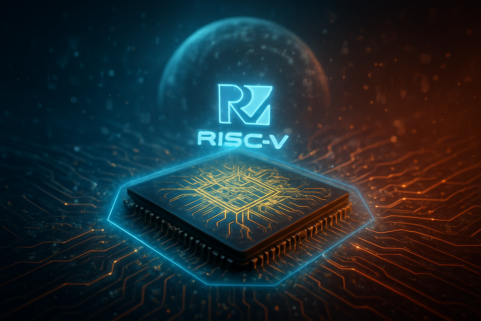
As the semiconductor landscape reaches a fever pitch in late 2025, the industry is witnessing a seismic shift in power away from proprietary instruction set architectures (ISAs). RISC-V, the open-source standard once dismissed as an academic curiosity, has officially transitioned into a cornerstone of global technology strategy. Driven by a desire to escape the restrictive licensing regimes of ARM Holdings (NASDAQ: ARM) and the escalating "silicon curtain" between the United States and China, tech giants are now treating RISC-V not just as an alternative, but as a mandatory insurance policy for the future of artificial intelligence.
The significance of this movement cannot be overstated. In a year defined by trillion-parameter models and massive data center expansions, the reliance on a single, UK-based licensing entity has become an unacceptable business risk for the world’s largest chip buyers. From the acquisition of specialized startups to the deployment of RISC-V-native AI PCs, the industry has signaled that the era of closed-door architecture is ending, replaced by a modular, community-driven framework that promises both sovereign independence and unprecedented technical flexibility.
Standardizing the Revolution: Technical Milestones and Performance Parity
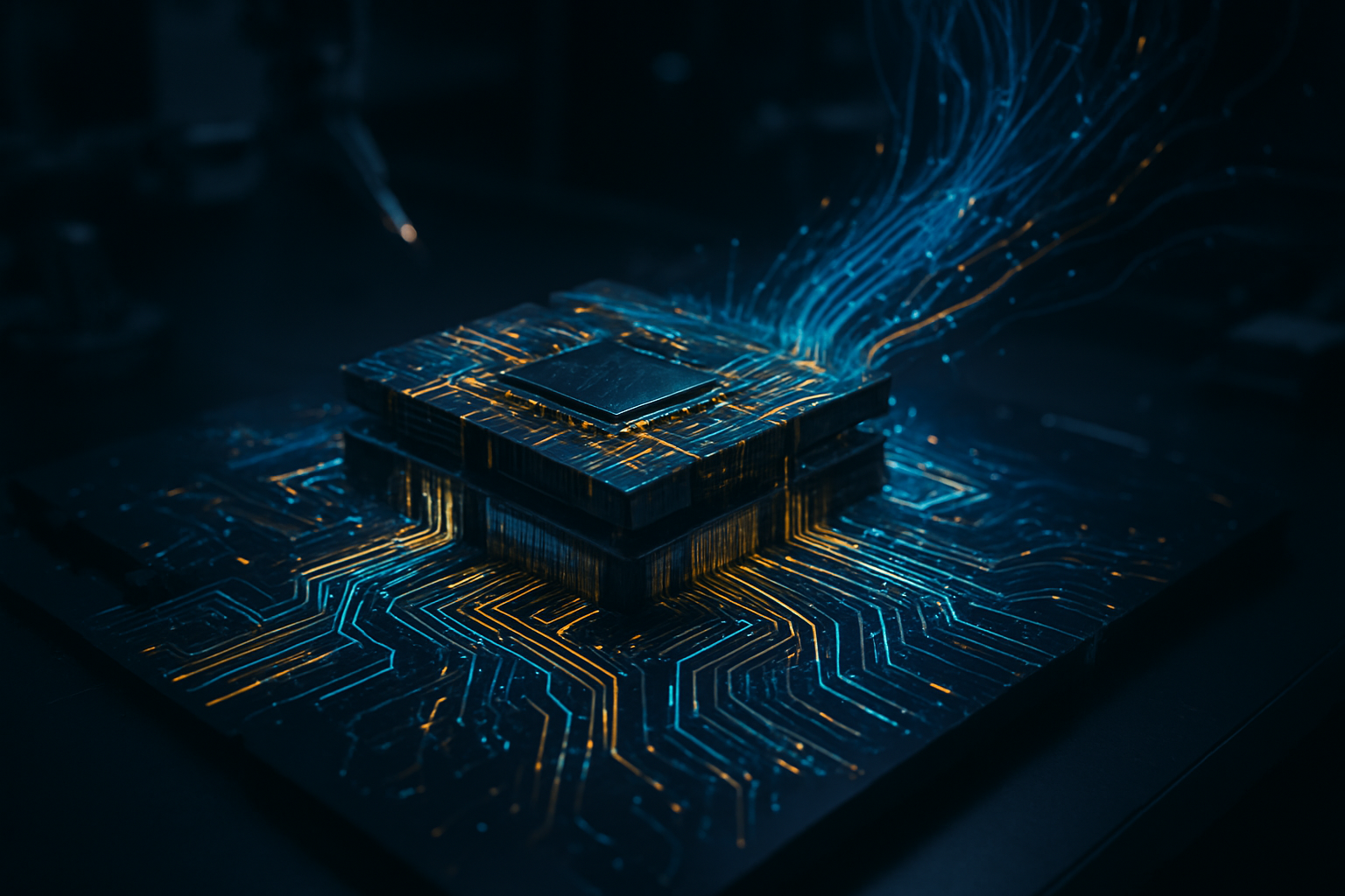
The technical narrative of RISC-V in 2025 is dominated by the ratification and widespread adoption of the RVA23 profile. Previously, the greatest criticism of RISC-V was its fragmentation—a "Wild West" of custom extensions that made software portability a nightmare. RVA23 has solved this by mandating standardized vector and hypervisor extensions, ensuring that major Linux distributions and AI frameworks can run natively across different silicon implementations. This standardization has paved the way for server-grade compatibility, allowing RISC-V to compete directly with ARM’s Neoverse and Intel’s (NASDAQ: INTC) x86 in the high-performance computing (HPC) space.
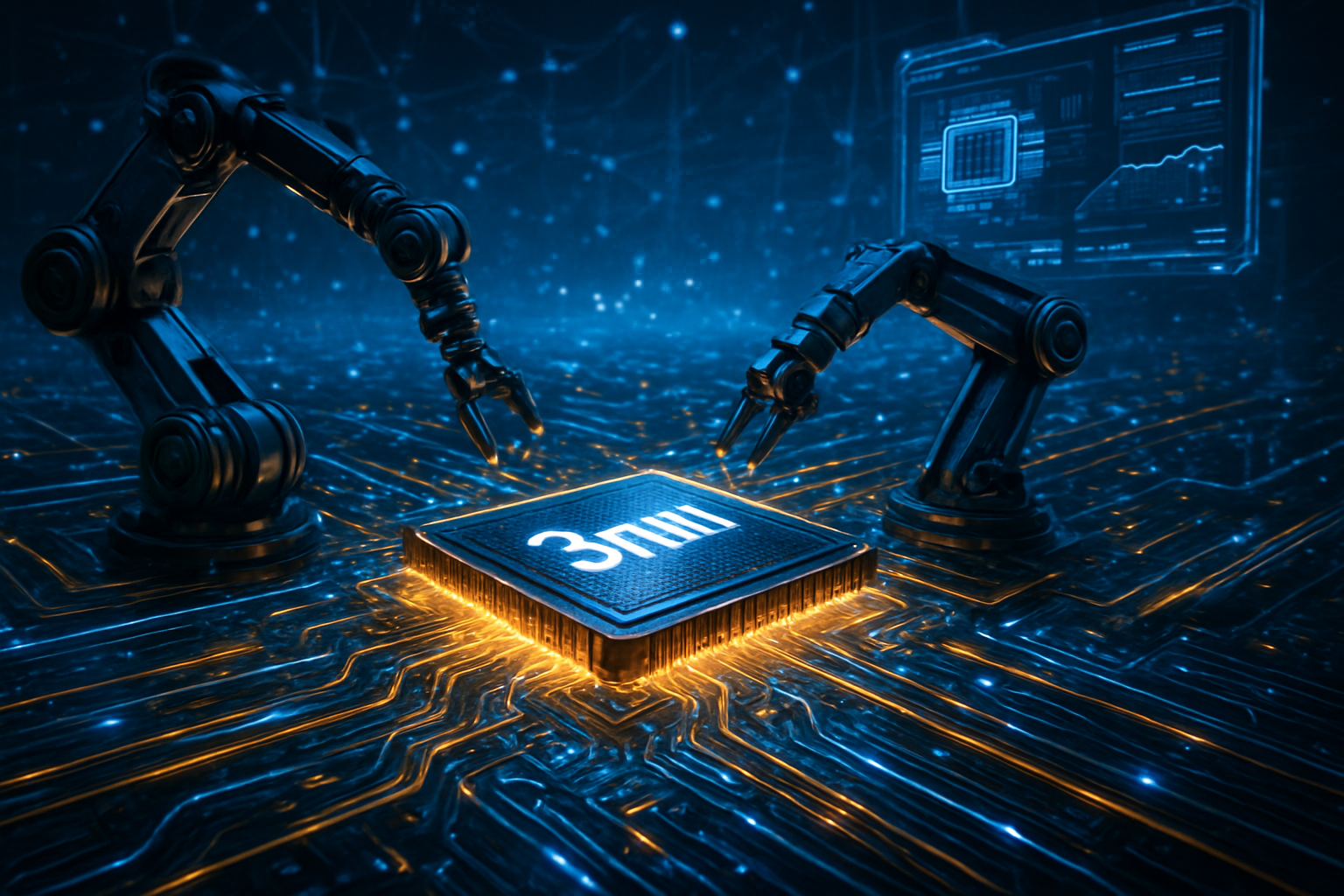
On the performance front, the gap between open-source and proprietary designs has effectively closed. SiFive’s recently launched 2nd Gen Intelligence family, featuring the X160 and X180 cores, has introduced dedicated Matrix engines specifically designed for the heavy lifting of AI training and inference. These cores are achieving performance benchmarks that rival mid-range x86 server offerings, but with significantly lower power envelopes. Furthermore, Tenstorrent’s "Ascalon" architecture has demonstrated parity with high-end Zen 5 performance in specific data center workloads, proving that RISC-V is no longer limited to low-power microcontrollers or IoT devices.
The reaction from the AI research community has been overwhelmingly positive. Researchers are particularly drawn to the "open-instruction" nature of RISC-V, which allows them to design custom instructions for specific AI kernels—something strictly forbidden under standard ARM licenses. This "hardware-software co-design" capability is seen as the key to unlocking the next generation of efficiency in Large Language Models (LLMs), as developers can now bake their most expensive mathematical operations directly into the silicon's logic.
The Strategic Hedge: Acquisitions and the End of the "Royalty Trap"
The business world’s pivot to RISC-V was accelerated by the legal drama surrounding the ARM vs. Qualcomm (NASDAQ: QCOM) lawsuit. Although a U.S. District Court in Delaware handed Qualcomm a complete victory in September 2025, dismissing ARM’s claims regarding Nuvia licenses, the damage to ARM’s reputation as a stable partner was already done. The industry viewed ARM’s attempt to cancel Qualcomm’s license on 60 days' notice as a "Sputnik moment," forcing every major player to evaluate their exposure to a single vendor’s legal whims.
In response, the M&A market for RISC-V talent has exploded. In December 2025, Qualcomm finalized its $2.4 billion acquisition of Ventana Micro Systems, a move designed to integrate high-performance RISC-V server-class cores into its "Oryon" roadmap. This provides Qualcomm with an "ARM-free" path for future data centers and automotive platforms. Similarly, Meta Platforms (NASDAQ: META) acquired the stealth startup Rivos for an estimated $2 billion to accelerate the development of its MTIA v2 (Artemis) inference chips. By late 2025, Meta’s internal AI infrastructure has already begun offloading scalar processing tasks to custom RISC-V cores, reducing its reliance on both ARM and NVIDIA (NASDAQ: NVDA).
Alphabet Inc. (NASDAQ: GOOGL) has also joined the fray through its RISE (RISC-V Software Ecosystem) project and a new "AI & RISC-V Gemini Credit" program. By incentivizing researchers to port AI software to RISC-V, Google is ensuring that its software stack remains architecture-agnostic. This strategic positioning allows these tech giants to negotiate from a position of power, using RISC-V as a credible threat to bypass traditional licensing fees that have historically eaten into their hardware margins.
The Silicon Divide: Geopolitics and Sovereign Computing
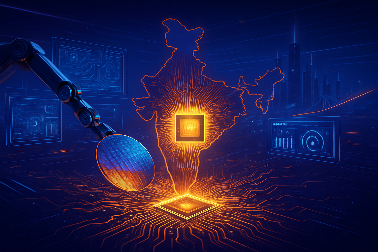
Beyond corporate boardrooms, RISC-V has become the central battleground in the ongoing tech war between the U.S. and China. For Beijing, RISC-V represents "Silicon Sovereignty"—a way to bypass U.S. export controls on x86 and ARM technologies. Alibaba Group (NYSE: BABA), through its T-Head semiconductor division, recently unveiled the XuanTie C930, a server-grade processor featuring 512-bit vector units optimized for AI. This development, alongside the open-source "Project XiangShan," has allowed Chinese firms to maintain a cutting-edge AI roadmap despite being cut off from Western proprietary IP.
However, this rapid progress has raised alarms in Washington. In December 2025, the U.S. Senate introduced the Secure and Feasible Export of Chips (SAFE) Act. This proposed legislation aims to restrict U.S. companies from contributing "advanced high-performance extensions"—such as matrix multiplication or specialized AI instructions—to the global RISC-V standard if those contributions could benefit "adversary nations." This has led to fears of a "bifurcated ISA," where the world’s computing standards split into a Western-aligned version and a China-centric version.
This potential forking of the architecture is a significant concern for the global supply chain. While RISC-V was intended to be a unifying force, the geopolitical reality of 2025 suggests it may instead become the foundation for two separate, incompatible tech ecosystems. This mirrors previous milestones in telecommunications where competing standards (like CDMA vs. GSM) slowed global adoption, yet the stakes here are much higher, involving the very foundation of artificial intelligence and national security.
The Road Ahead: AI-Native Silicon and Warehouse-Scale Clusters
Looking toward 2026 and beyond, the industry is preparing for the first "RISC-V native" data centers. Experts predict that within the next 24 months, we will see the deployment of "warehouse-scale" AI clusters where every component—from the CPU and GPU to the network interface card (NIC)—is powered by RISC-V. This total vertical integration will allow for unprecedented optimization of data movement, which remains the primary bottleneck in training massive AI models.
The consumer market is also on the verge of a breakthrough. Following the debut of the world’s first 50 TOPS RISC-V AI PC earlier this year, several major laptop manufacturers are rumored to be testing RISC-V-based "AI companions" for 2026 release. These devices will likely target the "local-first" AI market, where privacy-conscious users want to run LLMs entirely on-device without relying on cloud providers. The challenge remains the software ecosystem; while Linux support is robust, the porting of mainstream creative suites and gaming engines to RISC-V is still in its early stages.
A New Chapter in Computing History
The rising adoption of RISC-V in 2025 marks a definitive end to the era of architectural monopolies. What began as a project at UC Berkeley has evolved into a global movement that provides a vital escape hatch from the escalating costs of proprietary licensing and the unpredictable nature of international trade policy. The transition has been painful for some and expensive for others, but the result is a more resilient, competitive, and innovative semiconductor industry.
As we move into 2026, the key metrics to watch will be the progress of the SAFE Act in the U.S. and the speed at which the software ecosystem matures. If RISC-V can successfully navigate the geopolitical minefield without losing its status as a global standard, it will likely be remembered as the most significant development in computer architecture since the invention of the integrated circuit. For now, the message from the industry is clear: the future of AI will be open, modular, and—most importantly—under the control of those who build it.
This content is intended for informational purposes only and represents analysis of current AI developments.
TokenRing AI delivers enterprise-grade solutions for multi-agent AI workflow orchestration, AI-powered development tools, and seamless remote collaboration platforms.
For more information, visit https://www.tokenring.ai/.