As of December 19, 2025, the semiconductor industry has reached a definitive crossroads where the traditional laws of physics and the insatiable demands of artificial intelligence have finally collided. For decades, "Moore’s Law" was sustained by simply shrinking transistors on a two-dimensional plane, but the era of Large Language Models (LLMs) has pushed these classical manufacturing processes to their absolute breaking point. To prevent a total stagnation in AI performance, the world’s leading foundries have been forced to reinvent the very architecture of the silicon chip, moving from the decades-old FinFET design to radical new "Gate-All-Around" (GAA) structures and innovative power delivery systems.
This transition marks the most significant shift in microchip fabrication since the 1960s. As trillion-parameter models become the industry standard, the bottleneck is no longer just raw compute power, but the physical ability to deliver electricity to billions of transistors and dissipate the resulting heat without melting the silicon. The rollout of 2-nanometer (2nm) class nodes by late 2025 represents a "hail mary" for the AI industry, utilizing atomic-scale engineering to keep the promise of exponential intelligence alive.
The Death of the Fin: GAAFET and the 2nm Frontier
The technical centerpiece of this evolution is the industry-wide abandonment of the FinFET (Fin Field-Effect Transistor) in favor of Gate-All-Around (GAA) technology. In traditional FinFETs, the gate controlled the channel from three sides; however, at the 2nm scale, electrons began "leaking" out of the channel due to quantum tunneling, leading to massive power waste. The new GAA architecture—referred to as "Nanosheets" by TSMC (NYSE:TSM), "RibbonFET" by Intel (NASDAQ:INTC), and "MBCFET" by Samsung (KRX:005930)—wraps the gate entirely around the channel on all four sides. This provides total electrostatic control, allowing for higher clock speeds at lower voltages, which is essential for the high-duty-cycle matrix multiplications required by LLM inference.
Beyond the transistor itself, the most disruptive technical advancement of 2025 is Backside Power Delivery (BSPDN). Historically, chips were built like a house where the plumbing and electrical wiring were all crammed into the ceiling, creating a congested mess that blocked the "residents" (the transistors) from moving efficiently. Intel’s "PowerVia" and TSMC’s "Super Power Rail" have moved the entire power distribution network to the bottom of the silicon wafer. This decoupling of power and signal lines reduces voltage drops by up to 30% and frees up the top layers for the ultra-fast data interconnects that AI clusters crave.
Initial reactions from the AI research community have been overwhelmingly positive, though tempered by the sheer cost of these advancements. High-NA (Numerical Aperture) EUV lithography machines from ASML (NASDAQ:ASML), which are required to print these 2nm features, now cost upwards of $380 million each. Experts note that while these technologies solve the immediate "Power Wall," they introduce a new "Economic Wall," where only the largest hyperscalers can afford to design and manufacture the cutting-edge silicon necessary for next-generation frontier models.
The Foundry Wars: Who Wins the AI Hardware Race?
This technological shift has fundamentally rewired the competitive landscape for tech giants. NVIDIA (NASDAQ:NVDA) remains the primary beneficiary, as its upcoming "Rubin" R100 architecture is the first to fully leverage TSMC’s 2nm N2 process and advanced CoWoS-L (Chip-on-Wafer-on-Substrate) packaging. By stitching together multiple 2nm compute dies with the newly standardized HBM4 memory, NVIDIA has managed to maintain its lead in training efficiency, making it difficult for competitors to catch up on a performance-per-watt basis.
However, the 2nm era has also provided a massive opening for Intel. After years of trailing, Intel’s 18A (1.8nm) node has entered high-volume manufacturing at its Arizona fabs, successfully integrating both RibbonFET and PowerVia ahead of its rivals. This has allowed Intel to secure major foundry customers like Microsoft (NASDAQ:MSFT) and Amazon (NASDAQ:AMZN), who are increasingly looking to design their own custom AI ASICs (Application-Specific Integrated Circuits) to reduce their reliance on NVIDIA. The ability to offer "system-level" foundry services—combining 1.8nm logic with advanced 3D packaging—has positioned Intel as a formidable challenger to TSMC’s long-standing dominance.
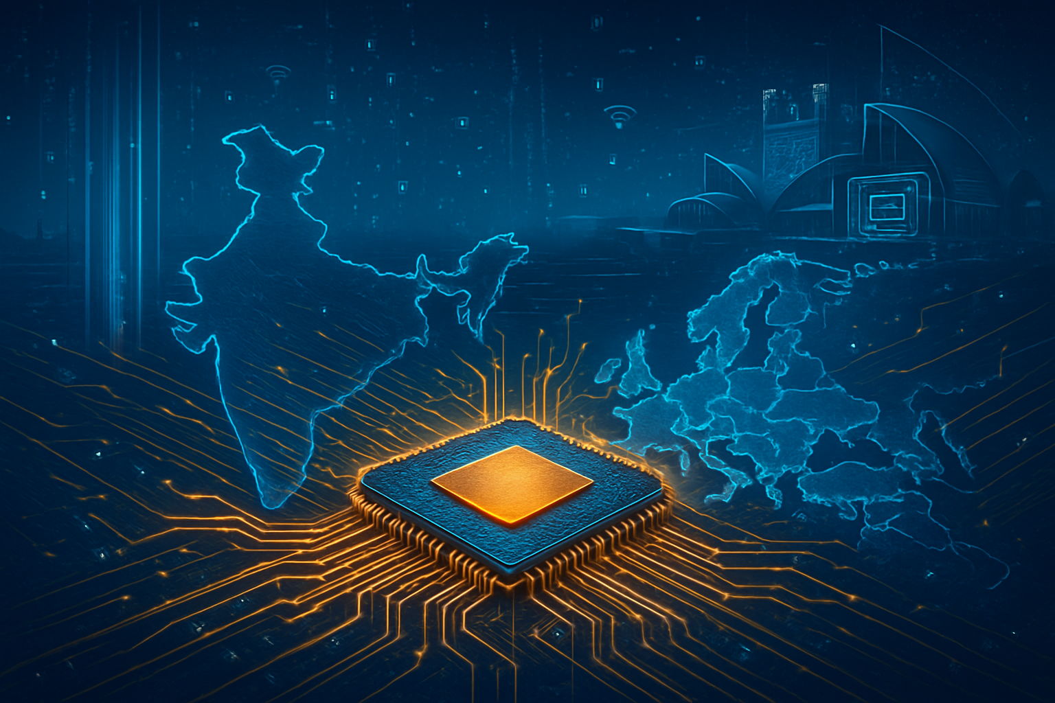
For startups and mid-tier AI companies, the implications are more double-edged. While the increased efficiency of 2nm chips may eventually lower the cost of API tokens for models like GPT-5 or Claude 4, the "barrier to entry" for building custom hardware has never been higher. The industry is seeing a consolidation of power, where the strategic advantage lies with companies that can secure guaranteed capacity at 2nm fabs. This has led to a flurry of long-term supply agreements and "pre-payments" for fab space, effectively turning silicon capacity into a form of geopolitical and corporate currency.
Beyond the Transistor: The Memory Wall and Sustainability
The evolution of CMOS for AI is not occurring in a vacuum; it is part of a broader trend toward "System-on-Package" (SoP) design. As transistors hit physical limits, the "Memory Wall"—the speed gap between the processor and the RAM—has become the primary bottleneck for LLMs. The response in 2025 has been the rapid adoption of HBM4 (High Bandwidth Memory), developed by leaders like SK Hynix (KRX:000660) and Micron (NASDAQ:MU). HBM4 utilizes a 2048-bit interface to provide over 2 terabytes per second of bandwidth, but it requires the same advanced packaging techniques used for 2nm logic, further blurring the line between chip design and manufacturing.
There are, however, significant concerns regarding the environmental impact of this hardware arms race. While 2nm chips are more power-efficient per operation, the sheer scale of the deployments means that total AI energy consumption continues to skyrocket. The manufacturing process for 2nm wafers is also significantly more water-and-chemical-intensive than previous generations. Critics argue that the industry is "running to stand still," using massive amounts of resources to achieve incremental gains in model performance that may eventually face diminishing returns.
Comparatively, this milestone is being viewed as the "Post-Silicon Era" transition. Much like the move from vacuum tubes to transistors, or from planar transistors to FinFETs, the shift to GAA and Backside Power represents a fundamental change in the building blocks of computation. It marks the moment when "Moore's Law" transitioned from a law of physics to a law of sophisticated 3D engineering and material science.
The Road to 14A and Glass Substrates
Looking ahead, the roadmap for AI silicon is already moving toward the 1.4nm (14A) node, expected to arrive around 2027. Experts predict that the next major breakthrough will involve the replacement of organic packaging materials with glass substrates. Companies like Intel and SK Absolics are currently piloting glass cores, which offer superior thermal stability and flatness. This will allow for even larger "gigascale" packages that can house dozens of chiplets and HBM stacks, essentially creating a "supercomputer on a single substrate."
Another area of intense research is the use of alternative metals like Ruthenium and Molybdenum for chip wiring. As copper wires become too thin and resistive at the 2nm level, these exotic metals will be required to keep signals moving at the speed of light. The challenge will be integrating these materials into the existing CMOS workflow without tanking yields. If successful, these developments could pave the way for AGI-scale hardware capable of trillion-parameter real-time reasoning.
Summary and Final Thoughts
The evolution of CMOS technology in late 2025 serves as a testament to human ingenuity in the face of physical limits. By transitioning to GAAFET architectures, implementing Backside Power Delivery, and embracing HBM4, the semiconductor industry has successfully extended the life of Moore’s Law for at least another decade. The key takeaway is that AI development is no longer just a software or algorithmic challenge; it is a deep-tech manufacturing challenge that requires the tightest possible integration between silicon design and fabrication.
In the history of AI, the 2nm transition will likely be remembered as the moment hardware became the ultimate gatekeeper of progress. While the performance gains are staggering, the concentration of this technology in the hands of a few global foundries and hyperscalers will continue to be a point of contention. In the coming weeks and months, the industry will be watching the yield rates of TSMC’s N2 and Intel’s 18A nodes closely, as these numbers will ultimately determine the pace of AI innovation through 2026 and beyond.
This content is intended for informational purposes only and represents analysis of current AI developments.
TokenRing AI delivers enterprise-grade solutions for multi-agent AI workflow orchestration, AI-powered development tools, and seamless remote collaboration platforms.
For more information, visit https://www.tokenring.ai/.