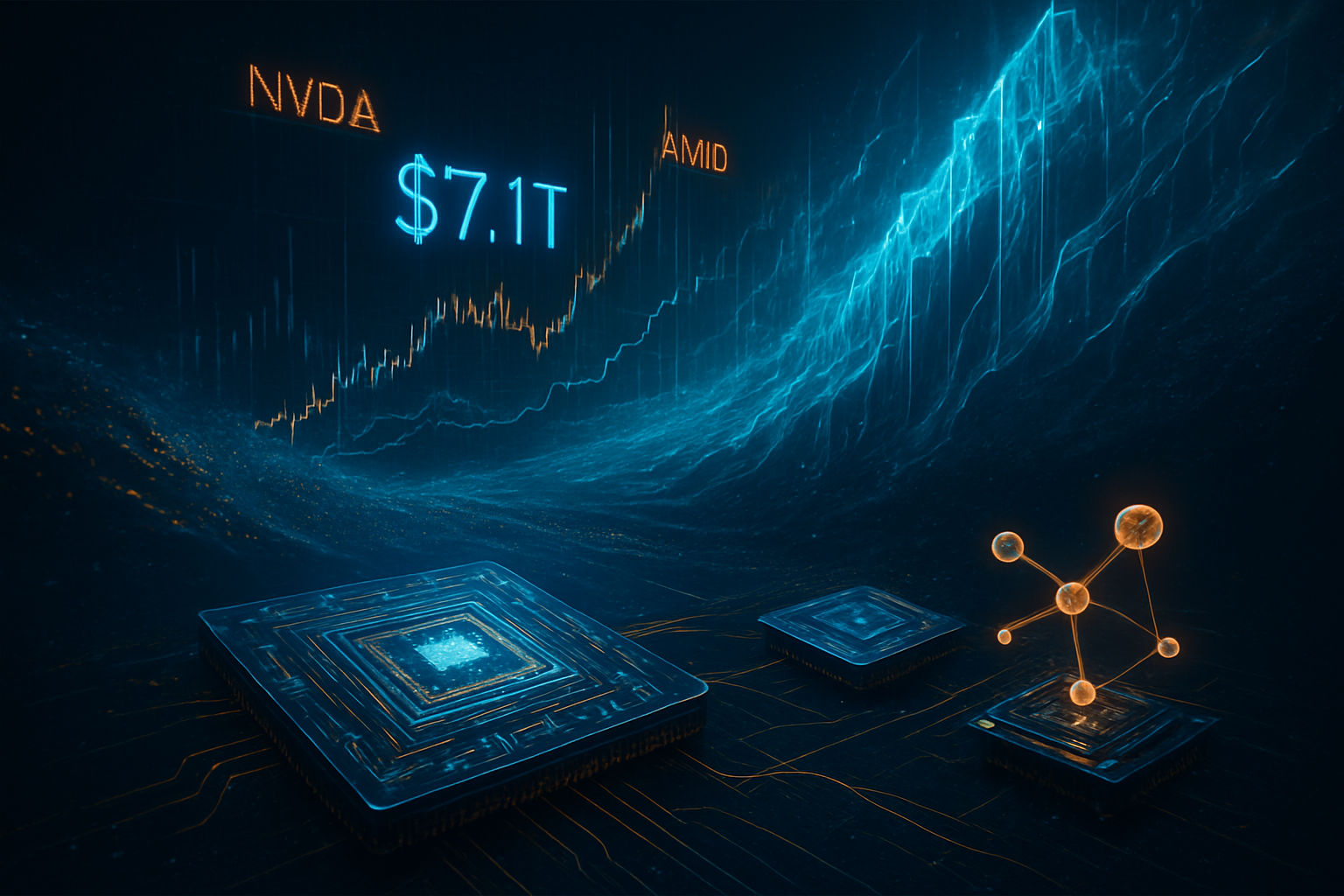
Tag: Semiconductors

  • LightPath Technologies Illuminates Specialized Optics Market with Strong Analyst Confidence Amidst Strategic Expansion

    LightPath Technologies Illuminates Specialized Optics Market with Strong Analyst Confidence Amidst Strategic Expansion

    Orlando, FL – December 17, 2025 – In a rapidly evolving semiconductor and specialized optics landscape, LightPath Technologies (NASDAQ: LPTH) is drawing significant attention from financial analysts, cementing its position as a pivotal player, particularly in defense and high-performance infrared (IR) applications. While specific details regarding a Roth Capital initiation of coverage were not broadly published, the broader market sentiment, exemplified by firms like Craig-Hallum initiating coverage with a "Buy" rating in April 2025 and subsequent "Buy" reiterations from HC Wainwright, Ladenburg Thalmann, and Lake Street Capital in November 2025, signals robust confidence in LightPath's strategic direction and proprietary technologies. This wave of positive outlook arrives as the company navigates a recent public offering of its Class A common stock in December 2025, aimed at bolstering its financial foundation for aggressive growth and strategic investments.

    The renewed focus on LightPath Technologies underscores a critical shift in the specialized optics sector, driven by escalating global demand for advanced sensing, thermal imaging, and secure supply chains. LightPath's unique material science and manufacturing capabilities are positioning it as an indispensable partner for defense contractors and innovators in emerging technological domains. The consensus among analysts points to LightPath's vertical integration, proprietary materials like BlackDiamond™ glass, and its strong pipeline of defense contracts as key drivers for future revenue growth and market penetration.

    Technical Prowess: BlackDiamond™ Glass and the Future of Infrared Optics

    LightPath Technologies stands out due to its proprietary BlackDiamond™ series of chalcogenide-based glasses, including BD2 and BD6, manufactured in its Orlando facility. These materials are not merely alternatives but represent a significant technical leap in infrared optics. Unlike traditional IR materials such as germanium, BlackDiamond™ glasses offer a broad transmission range from 0.5μm to 25μm, encompassing the critical short-wave (SWIR), mid-wave (MWIR), and long-wave infrared (LWIR) bands. This wide spectral coverage is crucial for next-generation multi-spectral imaging and sensing systems.

    A key differentiator lies in their superior thermal stability and ability to achieve passive athermalization. BlackDiamond™ glasses possess a low refractive index temperature coefficient (dN/dT) and low dispersion, allowing optical systems to maintain consistent performance across extreme temperature variations without requiring active thermal compensation. This characteristic is vital for demanding applications in aerospace, defense, and industrial environments where temperature fluctuations can severely degrade image quality and system reliability. Furthermore, these materials are engineered to withstand harsh mechanical conditions and are not susceptible to thermal runaway, a common issue with some IR materials.

    LightPath's manufacturing capabilities further enhance its technological edge. The company produces BlackDiamond™ glass in boules up to 120mm in diameter, utilizing proprietary molding technology for larger sizes. This precision glass molding process allows for the high-volume, cost-effective production of complex aspherical and freeform optics with tight tolerances, a significant advantage over the labor-intensive single-point diamond turning often required for traditional IR materials. The exclusive license from the U.S. Naval Research Laboratories (NRL) for new chalcogenide glasses like BDNL-4, featuring negative thermoptic coefficients, further solidifies LightPath's lead in advanced athermalized optical systems.

    This approach fundamentally differs from previous generations of IR optics, which heavily relied on germanium. Germanium's scarcity, high cost, and recent export restrictions from China have created significant supply chain vulnerabilities. LightPath's chalcogenide glass provides a readily available, stable, and cost-effective alternative, mitigating these risks and freeing up germanium for other critical semiconductor applications. The ability to customize the molecular composition of BlackDiamond™ glass also allows for tailored optical parameters, extending performance beyond what is typically achievable with off-the-shelf materials, thereby enabling miniaturization and Size, Weight, and Power (SWaP) optimization critical for modern platforms.

    Reshaping the Landscape for AI, Tech Giants, and Startups

    The advancements spearheaded by LightPath Technologies have profound implications for AI companies, tech giants, and innovative startups, particularly those operating in sensor-intensive domains. Companies developing advanced autonomous systems, such as self-driving vehicles (LiDAR), drones, and robotics, stand to benefit immensely from LightPath's high-performance, athermalized IR optics. The ability to integrate smaller, lighter, and more robust thermal imaging components can lead to more sophisticated sensor fusion capabilities, enhancing AI's perception in challenging environmental conditions, including low light, fog, and smoke.

    For defense contractors and aerospace giants, LightPath's solutions offer a critical competitive advantage. With approximately 70% of its revenues tied to the defense sector, the company's proprietary materials and vertical integration ensure a secure and independent supply chain, crucial in an era of geopolitical tensions and export controls. This mitigates risks associated with foreign-sourced materials and enables the development of next-generation night vision, missile guidance, surveillance, and counter-UAS systems without compromise. The substantial development contract with Lockheed Martin, for instance, highlights the trust placed in LightPath's capabilities.

    The disruption potential extends to existing products and services across various industries. Companies reliant on traditional, bulky, or thermally unstable IR optics may find themselves outmaneuvered by competitors adopting LightPath's advanced solutions, which enable miniaturization and enhanced performance. This could lead to a new generation of more compact, efficient, and reliable thermal cameras for industrial monitoring, medical diagnostics, and security applications. LightPath's market positioning as a vertically integrated solutions provider—from raw material development to complete IR camera systems—offers strategic advantages by ensuring end-to-end quality control and rapid innovation cycles for its partners.

    Wider Significance in the AI and Semiconductor Ecosystem

    LightPath Technologies' developments fit seamlessly into the broader AI and semiconductor landscape, particularly within the context of increasing demand for sophisticated sensing and perception capabilities. As AI systems become more prevalent in critical applications, the quality and reliability of input data from sensors become paramount. Advanced IR optics, such as those produced by LightPath, are essential for providing AI with robust visual data in conditions where traditional visible-light cameras fail, thereby enhancing the intelligence and resilience of autonomous platforms.

    The impact of LightPath's proprietary materials extends beyond mere component improvement; it addresses significant geopolitical and supply chain concerns. By utilizing proprietary BlackDiamond™ glass, LightPath can bypass export limitations on certain materials from countries like China and Russia. This strategic independence is vital for national security and ensures a stable supply of critical components for defense and other sensitive applications. It highlights a growing trend in the tech industry to localize critical manufacturing and material science to build more resilient supply chains.

    Potential concerns, however, include the inherent volatility of defense spending cycles and the competitive landscape for specialized optical materials. While LightPath's technology offers distinct advantages, continuous innovation and scaling production remain crucial. Comparisons to previous AI milestones underscore the foundational nature of such material science breakthroughs; just as advancements in silicon manufacturing propelled the digital age, innovations in specialized optics like BlackDiamond™ glass are enabling the next wave of advanced sensing and AI-driven applications. This development represents a critical step towards more robust, intelligent, and secure autonomous systems.

    The Horizon: Future Developments and Expert Predictions

    Looking ahead, the trajectory for LightPath Technologies and the specialized optics market appears robust. In the near term, experts predict an accelerated integration of LightPath's advanced IR optics into a wider array of defense platforms, driven by increased global defense spending and the proliferation of drone technology. The company's focus on complete IR camera systems, following the acquisition of G5 Infrared, suggests an expansion into higher-value solutions, enabling faster adoption by system integrators. Expect continued growth in industrial AI and IoT applications, where precise thermal monitoring and sensing are becoming indispensable for predictive maintenance and process optimization.

    Long-term developments are poised to see LightPath's technology playing a pivotal role in emerging fields. Potential applications on the horizon include enhanced vision systems for fully autonomous vehicles, where robust all-weather perception is crucial, and advanced augmented and virtual reality (AR/VR) headsets that could leverage sophisticated IR depth sensing for more immersive and interactive experiences. As quantum computing and secure communication systems evolve, the broad spectral transmission of chalcogenide glasses might also find niche applications.

    However, challenges remain. Scaling the production of highly specialized materials and maintaining a competitive edge against new material science innovations will be critical. Navigating the complex interplay of international trade policies and geopolitical dynamics will also be paramount. Experts predict a continued premium on companies that can offer secure, high-performance, and cost-effective specialized components. The market will likely see an increasing demand for integrated optical solutions that reduce SWaP and enhance system-level performance, areas where LightPath is already demonstrating leadership.

    A Strategic Enabler for the AI-Driven Future

    In summary, the positive analyst sentiment surrounding LightPath Technologies (NASDAQ: LPTH), bolstered by its proprietary BlackDiamond™ chalcogenide-based glass and vertically integrated manufacturing, marks it as a strategic enabler in the specialized optics and broader technology landscape. The company's ability to provide superior, athermalized infrared optics offers a critical advantage over traditional materials like germanium, addressing both performance limitations and supply chain vulnerabilities. This positions LightPath as an indispensable partner for defense, aerospace, and emerging AI applications that demand robust, high-performance sensing capabilities.

    This development's significance in AI history cannot be overstated. By providing the foundational optical components for advanced perception systems, LightPath is indirectly accelerating the development and deployment of more intelligent and resilient AI. Its impact resonates across national security, industrial efficiency, and the future of autonomous technologies. As the company strategically utilizes the capital from its December 2025 public offering, what to watch for in the coming weeks and months includes new contract announcements, further analyst updates, and the market's reaction to its continued expansion into higher-value integrated solutions. LightPath Technologies is not just manufacturing components; it is crafting the eyes for the next generation of intelligent machines.


    This content is intended for informational purposes only and represents analysis of current AI developments.

    TokenRing AI delivers enterprise-grade solutions for multi-agent AI workflow orchestration, AI-powered development tools, and seamless remote collaboration platforms.
    For more information, visit https://www.tokenring.ai/.

  • Tata’s Trillion-Dollar Bet: India’s Ascent in Global Electronics and AI-Driven Semiconductor Manufacturing

    Tata’s Trillion-Dollar Bet: India’s Ascent in Global Electronics and AI-Driven Semiconductor Manufacturing

    In a monumental strategic shift, the Tata Group, India's venerable conglomerate, is orchestrating a profound transformation in the global electronics and semiconductor landscape. With investments soaring into the tens of billions of dollars, Tata is not merely entering the high-tech manufacturing arena but is rapidly establishing India as a critical hub for advanced electronics assembly and semiconductor fabrication. This ambitious push, significantly underscored by its role in iPhone manufacturing and a landmark alliance with Intel (NASDAQ: INTC), signals India's determined leap towards technological self-reliance and its emergence as a formidable player in the global supply chain, with profound implications for the future of AI-powered devices.

    The immediate significance of Tata's endeavors is multifaceted. By acquiring Wistron Corp's iPhone manufacturing facility in November 2023 and a majority stake in Pegatron Technology India in January 2025, Tata Electronics has become the first Indian company to fully assemble iPhones, rapidly scaling its production capacity. Simultaneously, the group is constructing India's first semiconductor fabrication plant in Dholera, Gujarat, and an advanced Outsourced Semiconductor Assembly and Test (OSAT) facility in Jagiroad, Assam. These initiatives are not just about manufacturing; they represent India's strategic pivot to reduce its dependence on foreign imports, create a resilient domestic ecosystem, and position itself at the forefront of the next wave of technological innovation, particularly in artificial intelligence.

    Engineering India's Silicon Future: A Deep Dive into Tata's Technical Prowess

    Tata's technical strategy is a meticulously planned blueprint for end-to-end electronics and semiconductor manufacturing. The acquisition of Wistron's (TWSE: 3231) 44-acre iPhone assembly plant near Bengaluru, boasting eight production lines, was a pivotal move in November 2023. This facility, now rebranded as Tata Electronics Systems Solutions (TESS), has already commenced trial production for the upcoming iPhone 17 series and is projected to account for up to half of India's total iPhone output within the next two years. This rapid scaling is a testament to Tata's operational efficiency and Apple's (NASDAQ: AAPL) strategic imperative to diversify its manufacturing base.

    Beyond assembly, Tata's most impactful technical investments are in the foundational elements of modern electronics: semiconductors. The company is committing approximately $14 billion to its semiconductor ventures. The Dholera, Gujarat fabrication plant, a greenfield project in partnership with Taiwan's Powerchip Semiconductor Manufacturing Corporation (PSMC) (TWSE: 6770), is designed to produce up to 50,000 wafers per month at process nodes up to 28nm. This capability, anticipated to begin chip output around mid-2027, will cater to crucial sectors including AI, automotive, computing, and data storage. Concurrently, the OSAT facility in Jagiroad, Assam, representing an investment of around $3.2 billion, is expected to become operational by mid-2025, focusing on advanced packaging technologies like Wire Bond, Flip Chip, and Integrated Systems Packaging (ISP). This facility alone is projected to produce 48 million semiconductor chips per day.

    A recent and significant development in December 2025 was the strategic alliance between Tata Electronics and Intel (NASDAQ: INTC). Through a Memorandum of Understanding (MoU), the two giants will explore manufacturing and advanced packaging of Intel products at Tata's upcoming facilities. This partnership is particularly geared towards scaling AI-focused personal computing solutions for the Indian market, which is projected to be a global top-five market by 2030. This differs significantly from India's previous manufacturing landscape, which largely relied on assembling imported components. Tata's integrated approach aims to build indigenous capabilities from silicon to finished product, a monumental shift that has garnered enthusiastic reactions from industry experts who see it as a game-changer for India's technological autonomy.

    Reshaping the Tech Titans: Competitive Implications and Strategic Advantages

    Tata's aggressive expansion directly impacts several major players in the global technology ecosystem. Apple (NASDAQ: AAPL) is a primary beneficiary, gaining a crucial and rapidly scaling manufacturing partner outside of China. This diversification mitigates geopolitical risks, reduces potential tariff impacts, and strengthens its "Made in India" strategy, with Tata's output increasingly destined for the U.S. market. However, it also empowers Tata as a potential future competitor or an Original Design Manufacturer (ODM) that could broaden its client base.

    Intel (NASDAQ: INTC) stands to gain significantly from its partnership with Tata. By leveraging Tata's nascent fabrication and OSAT capabilities, Intel can enhance cost competitiveness, accelerate time-to-market, and improve operational agility for its products within India. The collaboration's focus on tailored AI PC solutions for the Indian market positions Intel to capitalize on India's burgeoning demand for AI-powered computing.

    For traditional Electronics Manufacturing Services (EMS) providers like Taiwan's Foxconn (TWSE: 2354) and Pegatron (TWSE: 4938), Tata's rise introduces heightened competition, particularly within India. While Foxconn remains a dominant player, Tata is rapidly consolidating its position through acquisitions and organic growth, becoming the only Indian company in Apple's iPhone assembly ecosystem. Other Indian manufacturers, while facing increased competition from Tata's scale, could also benefit from the development of a broader local supply chain and ecosystem.

    Globally, tech companies like Microsoft (NASDAQ: MSFT) and Dell (NYSE: DELL), seeking supply chain diversification, view Tata as a strategic advantage. Tata's potential to evolve into an ODM could offer them an integrated partner for a range of devices. The localized semiconductor manufacturing and advanced packaging capabilities, particularly with the Intel partnership's AI focus, will provide domestic access to critical hardware components, accelerating AI development within India and fostering a stronger indigenous AI ecosystem. Tata's vertical integration, government support through initiatives like the "India Semiconductor Mission," and access to India's vast domestic market provide it with formidable strategic advantages, potentially disrupting established manufacturing hubs and creating a more geo-resilient supply chain.

    India's Digital Dawn: Wider Significance in the Global AI Landscape

    Tata's audacious plunge into electronics and semiconductor manufacturing is more than a corporate expansion; it is a declaration of India's strategic intent to become a global technology powerhouse. This initiative is inextricably linked to the broader AI landscape, as the Intel partnership explicitly aims to expand AI-powered computing across India and scale tailored AI PC solutions. By manufacturing chips and assembling AI-enabled devices locally, Tata will support India's burgeoning AI sector, reducing costs, speeding up deployment, and fostering indigenous innovation in AI and machine learning across various industries.

    This strategic pivot directly addresses evolving global supply chain trends and geopolitical considerations. The push for an "India-based geo-resilient electronics and semiconductor supply chain" is a direct response to vulnerabilities exposed by pandemic-induced disruptions and escalating U.S.-China trade tensions. India, positioning itself as a stable democracy and reliable investment destination, aims to attract more international players and integrate itself as a credible participant in global chip production. Apple's increasing production in India, partly driven by the threat of U.S. tariffs on China-manufactured goods, exemplifies this geopolitical realignment.

    The impacts are profound: significant economic growth, the creation of tens of thousands of high-skilled jobs, and the transfer of advanced technology and expertise to India. This will reduce India's import dependence, transforming it from a major chip importer to a self-sufficient, export-capable semiconductor producer, thereby enhancing national security and economic stability. However, potential concerns include challenges in securing critical raw materials, the immense capital and talent required to compete with established global hubs like Taiwan and South Korea, and unique logistical challenges such as protecting the Assam OSAT plant from wildlife, which could affect precision manufacturing. Tata's endeavors are often compared to India's earlier success in smartphone manufacturing self-reliance, but this push into semiconductors and advanced electronics represents a more ambitious trajectory, aiming to establish India as a key player in foundational technologies that will drive future global innovation.

    The Horizon Ahead: Future Developments and Expert Predictions

    The coming years promise a flurry of activity and transformative developments stemming from Tata's strategic investments. In the near term, the Vemgal, Karnataka OSAT facility, operational since December 2023, will be complemented by the major greenfield OSAT facility in Jagiroad, Assam, scheduled for commercial production by mid-2025, with a staggering capacity of 48 million chips per day. Concurrently, the Dholera, Gujarat fabrication plant is in an intensive construction phase, with trial production anticipated in early 2027 and the first wafers rolling out by mid-2027. The Intel (NASDAQ: INTC) partnership will see early manufacturing and packaging of Intel products at these facilities, alongside the rapid scaling of AI PC solutions in India.

    In iPhone manufacturing, Tata Electronics Systems Solutions (TESS) is already engaged in trial production for the iPhone 17 series. Experts predict that Apple (NASDAQ: AAPL) aims to produce all iPhones for the U.S. market in India by 2026, with Tata Group being a critical partner in achieving this goal. Beyond iPhones, Tata's units could diversify into assembling other Apple products, further deepening India's integration into Apple's supply chain.

    Longer-term, Tata Electronics is building a vertically integrated ecosystem, expanding across the entire semiconductor and electronics value chain. This will foster indigenous development through collaborations with entities like MeitY's Centre for Development of Advanced Computing (C-DAC), creating a robust local semiconductor design and IP ecosystem. The chips and electronic components produced will serve a wide array of high-growth sectors, including AI-powered computing, electric vehicles, computing and data storage, consumer electronics, industrial and medical devices, defense, and wireless communication.

    Challenges remain, particularly in securing a robust supply chain for critical raw materials, addressing the talent shortage by training engineers in specialized fields, and navigating intense global competition. Infrastructure and environmental factors, such as protecting the Assam plant from ground vibrations caused by elephants, also pose unique hurdles. Experts predict India's rising share in global electronics manufacturing, surpassing Vietnam as the world's second-largest exporter of mobile phones by FY26. The Intel-Tata partnership is expected to make India a top-five global market for AI PCs before 2030, contributing significantly to India's digital autonomy and achieving 35% domestic value addition in its electronics manufacturing ecosystem by 2030.

    A New Dawn for India's Tech Ambitions: The Trillion-Dollar Trajectory

    Tata Group's aggressive and strategic investments in electronics assembly and semiconductor manufacturing represent a watershed moment in India's industrial history. By becoming a key player in iPhone manufacturing and forging a landmark partnership with Intel (NASDAQ: INTC) for chip fabrication and AI-powered computing, Tata is not merely participating in the global technology sector but actively reshaping it. This comprehensive initiative, backed by the Indian government's "India Semiconductor Mission" and Production Linked Incentive (PLI) schemes, is poised to transform India into a formidable global hub for high-tech manufacturing, reducing import reliance and fostering digital autonomy.

    The significance of this development in AI history cannot be overstated. The localized production of advanced silicon, especially for AI applications, will accelerate AI development and adoption within India, fostering a stronger domestic AI ecosystem and potentially leading to new indigenous AI innovations. It marks a crucial step in democratizing access to cutting-edge hardware essential for the proliferation of AI across industries.

    In the coming weeks and months, all eyes will be on the progress of Tata's Dholera fab and Assam OSAT facilities, as well as the initial outcomes of the Intel partnership. The successful operationalization and scaling of these ventures will be critical indicators of India's capacity to execute its ambitious technological vision. This is a long-term play, but one that promises to fundamentally alter global supply chains, empower India's economic growth, and cement its position as a vital contributor to the future of artificial intelligence and advanced electronics.


    This content is intended for informational purposes only and represents analysis of current AI developments.

    TokenRing AI delivers enterprise-grade solutions for multi-agent AI workflow orchestration, AI-powered development tools, and seamless remote collaboration platforms.
    For more information, visit https://www.tokenring.ai/.

  • China’s “Manhattan Project” Unveils EUV Prototype, Reshaping Global Chip Landscape

    China’s “Manhattan Project” Unveils EUV Prototype, Reshaping Global Chip Landscape

    In a development poised to dramatically reshape the global semiconductor industry, China has reportedly completed a prototype Extreme Ultraviolet (EUV) lithography machine, marking a significant leap in its ambitious "Manhattan Project" to achieve chip sovereignty. This technological breakthrough, confirmed by reports in early 2025, signifies a direct challenge to the long-standing monopoly held by Dutch giant ASML Holding N.V. (AMS: ASML) in the advanced chipmaking arena. The immediate significance of this achievement cannot be overstated: it represents a critical step for Beijing in bypassing stringent US-led export controls and securing an independent supply chain for the cutting-edge semiconductors vital for artificial intelligence, 5G, and advanced military applications.

    The initiative, characterized by its secrecy, state-driven funding, and a "whole-of-nation" approach, underscores China's unwavering commitment to technological self-reliance. While the prototype has successfully generated EUV light—the essential ingredient for advanced chipmaking—it has yet to produce functional chips. Nevertheless, its existence alone signals China's potential to disrupt the delicate balance of power in the tech world, demonstrating a resolve to overcome external dependencies and establish itself as a formidable player at the forefront of semiconductor innovation.

    Technical Prowess and the Road Less Traveled

    The completion of China's prototype EUV lithography machine in early 2025, within a highly secure laboratory in Shenzhen, represents a monumental engineering feat. This colossal apparatus, sprawling across nearly an entire factory floor, is currently undergoing rigorous testing. The core achievement lies in its ability to generate extreme ultraviolet light, a fundamental requirement for etching the minuscule patterns on silicon wafers that form advanced chips. While ASML's commercial EUV systems utilize a Laser Produced Plasma (LPP) light source, reports indicate that Chinese electronics giant Huawei Technologies Co., Ltd. (SHE: 002502) is actively testing an alternative Laser Discharge Induced Plasma (LDP) light source at its Dongguan facility, with trial production of circuits reportedly commencing in the third quarter of 2025. This LDP method is even speculated by some experts to potentially offer greater efficiency than ASML's established LPP technology.

    The development effort has reportedly been bolstered by a team comprising former engineers from ASML, who are believed to have reverse-engineered critical aspects of the Dutch firm's technology. To circumvent export restrictions, China has resourcefuly sourced parts from older ASML machines available on secondary markets, alongside components from Japanese suppliers like Nikon Corp. (TYO: 7731) and Canon Inc. (TYO: 7751). However, a key challenge remains the acquisition of high-precision optical systems, traditionally supplied by specialized firms like Germany's Carl Zeiss AG, a crucial ASML partner. This reliance on alternative sourcing and reverse engineering has resulted in a prototype that is reportedly significantly larger and less refined than ASML's commercial offerings.

    Despite these hurdles, the functionality of the Chinese prototype in generating EUV light marks a critical divergence from previous approaches, which primarily relied on Deep Ultraviolet (DUV) lithography combined with complex multi-patterning techniques to achieve smaller nodes—a method fraught with yield challenges. While ASML CEO Christophe Fouquet stated in April 2025 that China would need "many, many years" to develop such technology, the swift emergence of this prototype suggests a significantly accelerated timeline. China's ambitious target is to produce working chips from its domestic EUV machine by 2028, with 2030 being considered a more realistic timeframe by many industry observers. This indigenous development promises to free Chinese chipmakers from the technological stagnation imposed by international sanctions, offering a pathway to genuinely compete at the leading edge of semiconductor manufacturing.

    Shifting Tides: Competitive Implications for Global Tech Giants

    China's accelerated progress in domestic EUV lithography, spearheaded by Huawei Technologies Co., Ltd. (SHE: 002502) and Semiconductor Manufacturing International Corporation (SMIC) (HKG: 0981), is poised to trigger a significant reordering of the global technology landscape. The most immediate beneficiaries are Chinese semiconductor manufacturers and tech giants. SMIC, for instance, is reportedly on track to finalize its 5nm chip development by the end of 2025, with Huawei planning to leverage this advanced process for its Ascend 910C AI chip. Huawei itself is aggressively scaling its Ascend AI chip production, aiming to double output in 2025 to approximately 600,000 units, with plans to further increase total output to as many as 1.6 million dies in 2026. This domestic capability will provide a reliable, sanction-proof source of high-performance chips for Chinese tech companies like Alibaba Group Holding Ltd. (NYSE: BABA), DeepSeek, Tencent Holdings Ltd. (HKG: 0700), and Baidu, Inc. (NASDAQ: BIDU), ensuring the continuity and expansion of their AI operations and cloud services within China. Furthermore, the availability of advanced domestic chips is expected to foster a more vibrant ecosystem for Chinese AI startups, potentially lowering entry barriers and accelerating indigenous innovation.

    The competitive implications for Western chipmakers are profound. Companies like NVIDIA Corporation (NASDAQ: NVDA), Advanced Micro Devices, Inc. (NASDAQ: AMD), and Intel Corporation (NASDAQ: INTC), which have historically dominated the high-performance chip market, face a long-term threat to their market share within China and potentially beyond. While NVIDIA's newest Grace Blackwell series processors are seeing strong global demand, its dominance in China is demonstrably weakening due to export controls and the rapid ascent of Huawei's Ascend processors. Reports from early 2025 even suggested that some Chinese-designed AI accelerators were processing complex algorithms more efficiently than certain NVIDIA offerings. If China successfully scales its domestic EUV production, it could bypass Western restrictions on cutting-edge nodes (e.g., 5nm, 3nm), directly impacting the revenue streams of these global leaders.

    Global foundries like Taiwan Semiconductor Manufacturing Company Limited (TSMC) (NYSE: TSM) and Samsung Electronics Co., Ltd. (KRX: 005930), currently at the forefront of advanced chip manufacturing with ASML's EUV machines, could also face increased competition from SMIC. While SMIC's 5nm wafer costs are presently estimated to be up to 50% higher than TSMC's, coupled with lower yields due to its reliance on DUV for these nodes, successful domestic EUV implementation could significantly narrow this gap. For ASML Holding N.V. (AMS: ASML), the current undisputed monarch of EUV technology, China's commercialization of LDP-based EUV would directly challenge its monopoly. ASML CEO Christophe Fouquet has acknowledged that "China will not accept to be cut off from technology," highlighting the inevitability of China's pursuit of self-sufficiency. This intense competition is likely to accelerate efforts among global tech companies to diversify supply chains, potentially leading to a "decoupling" of technological ecosystems and the emergence of distinct standards and suppliers in China.

    Strategically, China's domestic EUV breakthrough grants it unparalleled technological autonomy and national security in advanced semiconductor manufacturing, aligning with the core objectives of its "Made in China 2025" initiative. Huawei, at the helm of this national strategy, is actively building a parallel, independent ecosystem for AI infrastructure, demonstrating a commitment to compensating for limited Western EUV access through alternative architectural strategies and massive domestic production scaling. This geopolitical rebalancing underscores that strategic pressure and export controls can, paradoxically, accelerate indigenous innovation. The success of China's EUV project will likely force a re-evaluation of current export control policies by the US and its allies, as the world grapples with the implications of a truly self-reliant Chinese semiconductor industry.

    A New Epoch: Broader Implications for the AI Landscape and Geopolitics

    The emergence of China's prototype EUV lithography machine in late 2025 is more than just a technical achievement; it is a foundational hardware breakthrough that will profoundly influence the broader Artificial Intelligence landscape and global geopolitical dynamics. EUV lithography is the linchpin for manufacturing the high-performance, energy-efficient chips with sub-7nm, 5nm, 3nm, and even sub-2nm nodes that are indispensable for powering modern AI applications—from sophisticated AI accelerators and neural processing units to large language models and advanced AI hardware for data centers, autonomous systems, and military technologies. Without such advanced manufacturing capabilities, the rapid advancements observed in AI development would face insurmountable obstacles. China's domestic EUV effort is thus a cornerstone of its strategy to achieve self-sufficiency in AI, mitigate the impact of U.S. export controls, and accelerate its indigenous AI research and deployment, effectively securing the "compute" power that has become the defining constraint for AI progress.

    The successful development and eventual mass production of China's EUV lithography machine carries multifaceted impacts. Geopolitically and economically, it promises to significantly reduce China's dependence on foreign technology, particularly ASML Holding N.V.'s (AMS: ASML) EUV systems, thereby enhancing its national security and resilience against export restrictions. This breakthrough could fundamentally alter the global technological balance, intensifying the ongoing "tech cold war" and challenging the West's historical monopoly on cutting-edge chipmaking technology. While it poses a potential threat to ASML's market dominance, it could also introduce new competition in the high-end lithography market, leading to shifts in global supply chains. However, the dual-use potential of advanced AI chips—serving both commercial and military applications—raises significant concerns and could further fuel geopolitical tensions regarding military-technological parity. Technologically, domestic access to EUV would enable China to produce its own cutting-edge AI chips, accelerating its progress in AI research, hardware development, and deployment across various sectors, facilitating new AI hardware architectures crucial for optimizing AI workloads, and potentially narrowing the node gap with leading manufacturers to 5nm, 3nm, or even 2nm by 2030.

    Despite the strategic advantages for China, this development also brings forth several concerns. The technical viability and quality of scaling production, ensuring sustained reliability, achieving comparable throughput, and replicating the precision optical systems of ASML's machines remain significant hurdles. Moreover, the reported reverse-engineering of ASML technology raises intellectual property infringement concerns. Geopolitical escalation is another real risk, as China's success could provoke further export controls and trade restrictions from the U.S. and its allies. The energy consumption of EUV lithography, an incredibly power-intensive process, also poses sustainability challenges as China ramps up its chip production. Furthermore, a faster, unrestrained acceleration of AI development in China, potentially without robust international ethical frameworks, could lead to novel ethical dilemmas and risks on a global scale.

    In the broader context of AI milestones, China's prototype EUV machine can be seen as a foundational hardware breakthrough, akin to previous pivotal moments. Just as powerful GPUs from companies like NVIDIA Corporation (NASDAQ: NVDA) provided the computational backbone for the deep learning revolution, EUV lithography acts as the "unseen engine" that enables the complex designs and high transistor densities required for sophisticated AI algorithms. This intense global investment in advanced chip manufacturing and AI infrastructure mirrors the scale of the dot-com boom or the expansion of cloud computing infrastructure. The fierce competition over AI chips and underlying manufacturing technology like EUV reflects a modern-day scramble for vital strategic resources. The U.S.-China AI rivalry, driven by the race for technological supremacy, is frequently compared to the nuclear arms race of the Cold War era. China's rapid progress in EUV lithography, spurred by export controls, exemplifies how strategic pressure can accelerate domestic innovation in critical technologies, a "DeepSeek moment for lithography" that parallels how Chinese AI models have rapidly caught up to and even rivaled leading Western models despite chip restrictions. This monumental effort underscores a profound shift in the global semiconductor and AI landscapes, intensifying geopolitical competition and potentially reshaping supply chains for decades to come.

    The Road Ahead: China's Ambitions and the Future of Advanced Chipmaking

    The journey from a prototype EUV lithography machine to commercially viable, mass-produced advanced chips is fraught with challenges, yet China's trajectory indicates a determined march towards its goals. In the near term, the focus is squarely on transitioning from successful EUV light generation to the production of functional chips. With a prototype already undergoing testing at facilities like Huawei Technologies Co., Ltd.'s (SHE: 002502) Dongguan plant, the critical next steps involve optimizing the entire manufacturing process. Trial production of circuits using these domestic systems reportedly commenced in the second or third quarter of 2025, with ambitious plans for full-scale or mass production slated for 2026. This period will be crucial for refining the Laser-Induced Discharge Plasma (LDP) method, which Chinese institutions like the Harbin Institute of Technology and the Shanghai Institute of Optics and Fine Mechanics are championing as an alternative to ASML Holding N.V.'s (AMS: ASML) Laser-Produced Plasma (LPP) technology. Success in this phase would validate the LDP approach and potentially offer a simpler, more cost-effective, and energy-efficient pathway to EUV.

    Looking further ahead, China aims to produce functional chips from its EUV prototypes by 2028, with 2030 being a more realistic target for achieving significant commercial output. The long-term vision is nothing less than complete self-sufficiency in advanced chip manufacturing. Should China successfully commercialize LDP-based EUV lithography, it would become the only nation outside the Netherlands with such advanced capabilities, fundamentally disrupting the global semiconductor industry. Experts predict that if China can advance to 3nm or even 2nm chip production by 2030, it could emerge as a formidable competitor to established leaders like ASML, Taiwan Semiconductor Manufacturing Company Limited (TSMC) (NYSE: TSM), and Samsung Electronics Co., Ltd. (KRX: 005930). This would unlock the domestic manufacturing of chips smaller than 7 nanometers, crucial for powering advanced Artificial Intelligence (AI) systems, military applications, next-generation smartphones, and high-performance computing, thereby significantly strengthening China's position in these strategic sectors.

    However, the path to commercial viability is riddled with formidable challenges. Technical optimization remains paramount, particularly in boosting the power output of LDP systems, which currently range from 50-100W but require at least 250W for commercial scale. Replicating the extreme precision of Western optical systems, especially those from Carl Zeiss AG, and developing a comprehensive domestic ecosystem for all critical components—including pellicles, masks, and resist materials—are significant bottlenecks. System integration, given the immense complexity of an EUV scanner, also presents considerable engineering hurdles. Beyond the technical, geopolitical and supply chain restrictions continue to loom, with the risk of further export controls on essential materials and components. While China has leveraged parts from older ASML machines obtained from secondary markets, this approach may not be sustainable or scalable for cutting-edge nodes.

    Expert predictions, while acknowledging China's remarkable progress, largely agree that scaling EUV production to commercially competitive levels will take considerable time. While some researchers, including those from TSMC, have optimistically suggested that China's LDP method could "out-compete ASML," most analysts believe that initial production capacity will likely be constrained. The unwavering commitment of the Chinese government, often likened to a "Manhattan Project," coupled with substantial investments and coordinated efforts across various research institutes and companies like Huawei, is a powerful driving force. This integrated approach, encompassing chip design to fabrication equipment, aims to entirely bypass foreign tech restrictions. The rate of China's progress towards self-sufficiency in advanced semiconductors will ultimately be determined by its ability to overcome these technological complexities and market dynamics, rather than solely by the impact of export controls, fundamentally reshaping the global semiconductor landscape in the coming years.

    The Dawn of a New Era: A Comprehensive Wrap-up

    China's "Manhattan Project" to develop a domestic EUV lithography machine has culminated in the successful creation of a working prototype, a monumental achievement that, as of December 2025, signals a pivotal moment in the global technology race. This breakthrough, driven by an unwavering national imperative for chip sovereignty, represents a direct response to stringent U.S.-led export controls and a strategic move to secure an independent supply chain for advanced semiconductors. Key takeaways include the prototype's ability to generate extreme ultraviolet light, its reliance on a combination of reverse engineering from older ASML Holding N.V. (AMS: ASML) machines, and the innovative adoption of Laser-Induced Discharge Plasma (LDP) technology, which some experts believe could offer advantages over ASML's LPP method. Huawei Technologies Co., Ltd. (SHE: 002502) stands at the forefront of this coordinated national effort, aiming to establish an entire domestic AI supply chain. While the prototype has yet to produce functional chips, with targets set for 2028 and a more realistic outlook of 2030, the progress is undeniable.

    This development holds immense significance in the history of Artificial Intelligence. Advanced AI systems, particularly those underpinning large language models and complex neural networks, demand cutting-edge chips with unparalleled processing power and efficiency—chips predominantly manufactured using EUV lithography. China's ability to master this technology and produce advanced chips domestically would dramatically reduce its strategic dependence on foreign suppliers for the foundational hardware of AI. This would not only enable China to accelerate its AI development independently, free from external bottlenecks, but also potentially shift the global balance of power in AI research and application, bolstering Beijing's quest for leadership in AI and military-technological parity.

    The long-term impact of China's EUV lithography project is poised to be profound and transformative. Should China successfully transition from a functional prototype to commercial-scale production of advanced chips by 2030, it would fundamentally redefine global semiconductor supply chains, challenging ASML's near-monopoly and ushering in a more multipolar semiconductor industry. This achievement would represent a major victory in China's "Made in China 2025" and subsequent self-reliance initiatives, significantly reducing its vulnerability to foreign export controls. While accelerating China's AI development, such a breakthrough is also likely to intensify geopolitical tensions, potentially prompting further countermeasures and heightened competition in the tech sphere.

    In the coming weeks and months, the world will be closely watching for several critical indicators. The most immediate milestone is the prototype's transition from generating EUV light to successfully producing working semiconductor chips, with performance metrics such as resolution capabilities, throughput stability, and yield rates being crucial. Further advancements in LDP technology, particularly in efficiency and power output, will demonstrate China's capacity for innovation beyond reverse-engineering. The specifics of China's 15th five-year plan (2026-2030), expected to be fully detailed next year, will reveal the continued scale of investment and strategic focus on semiconductor and AI self-reliance. Finally, any new export controls or diplomatic discussions from the U.S. and its allies in response to China's demonstrated progress will be closely scrutinized, as the global tech landscape continues to navigate this new era of intensified competition and technological independence.


    This content is intended for informational purposes only and represents analysis of current AI developments.

    TokenRing AI delivers enterprise-grade solutions for multi-agent AI workflow orchestration, AI-powered development tools, and seamless remote collaboration platforms.
    For more information, visit https://www.tokenring.ai/.

  • OMNIVISION’s Breakthrough Microdisplay Powers the Next Generation of AR/VR and the Metaverse

    OMNIVISION’s Breakthrough Microdisplay Powers the Next Generation of AR/VR and the Metaverse

    In a significant leap for wearable technology, OMNIVISION (NASDAQ: OV), a leading global developer of semiconductor solutions, has unveiled its OP03021, heralded as the industry's lowest-power single-chip full-color sequential microdisplay. Announced on December 16, 2025, this Liquid Crystal on Silicon (LCOS) panel is poised to revolutionize augmented reality (AR) and virtual reality (VR) smart glasses, laying crucial groundwork for the widespread adoption of the metaverse. By integrating the array, driver, and memory into an ultra-low-power, single-chip architecture, OMNIVISION is addressing critical hurdles in device size, comfort, and battery life, paving the way for AR smart glasses to become as ubiquitous as smartphones.

    This groundbreaking development promises to transform AR/VR devices from niche gadgets into mainstream consumer products. The immediate significance lies in enabling more fashionable, lightweight, and comfortable smart glasses that can be worn throughout the day. This enhanced user experience, coupled with higher resolution and an expanded field of view, is essential for delivering truly immersive and realistic augmented reality, which is a foundational element for seamless interaction within the persistent, shared virtual spaces of the metaverse.

    Technical Prowess: A Single Chip Redefines AR/VR Displays

    The OMNIVISION OP03021 microdisplay boasts impressive technical specifications designed to elevate immersive experiences. It delivers a high resolution of 1632 x 1536 pixels at a 90 Hz refresh rate within a compact 0.26-inch optical format, utilizing a small 3.0-micron pixel pitch. As a full-color sequential LCOS panel, it can support up to six color fields, ensuring stable, crisp, and clear visuals without image retention. The device features a MIPI-C-PHY 1-trio interface for data input and comes in a small Flexible Printed Circuit Array (FPCA) package, further contributing to its compact form factor.

    What truly differentiates the OP03021 is its single-chip, integrated LCOS architecture. Unlike conventional AR/VR display setups that often rely on multiple chips, the OP03021 integrates the pixel array, driver circuitry, and frame buffer memory directly onto a single silicon backplane. This "all-in-one" approach is touted as the industry's only single-chip LCOS small panel with ultra-low power for next-generation smart glasses. This comprehensive integration significantly reduces the overall size and power consumption of the microdisplay system, with OMNIVISION stating it can reduce power consumption by up to 40% compared to conventional two-chip solutions. This efficiency is paramount for battery-powered AR/VR glasses, allowing for longer usage times and reduced heat generation. The integrated design also simplifies the overall system for manufacturers, potentially leading to more compact and cost-effective devices.

    Initial reactions from industry experts have been highly positive. Devang Patel, Marketing Director for the IoT and emerging segment at OMNIVISION, emphasized the combination of increased resolution, expanded field of view, and the efficiency of the low-power, single-chip design. He stated that this "ultra-small, yet powerful, LCOS panel is a key feature in smart glasses that helps to make them more fashionable, lightweight and comfortable to wear throughout the day." Karl Guttag, President of KGOnTech and a recognized display industry expert, affirmed the technical advantages, noting that the integrated control, frame buffer memory, and MIPI receiver on the silicon backplane are critical factors for smart glass designs. Samples of the OP03021 are currently available, with mass production anticipated in the first half of 2026.

    Reshaping the Competitive Landscape for AI and Tech Giants

    The OMNIVISION OP03021 microdisplay is set to profoundly impact the competitive dynamics among AI companies, tech giants, and startups in the AR/VR and metaverse sectors. Its advancements in power efficiency, resolution, and form factor provide a crucial component for the next wave of immersive devices.

    For AI companies, the higher resolution and wider field of view enabled by the OP03021 directly enhance the visual input for sophisticated computer vision tasks. This allows for more accurate object recognition, environmental mapping (SLAM – Simultaneous Localization and Mapping), and gesture tracking, feeding more robust AI models. AI companies focused on contextual AI, advanced analytics, and realistic digital assistants for immersive experiences will find the improved display quality vital for rendering their AI-generated content convincingly. OMNIVISION itself provides image sensors and solutions for AR/VR applications, including Global Shutter cameras for eye tracking and SLAM, further highlighting the synergy between their display and sensor technologies.

    Tech giants such as Apple (NASDAQ: AAPL), Meta Platforms (NASDAQ: META), Alphabet (NASDAQ: GOOGL), and Microsoft (NASDAQ: MSFT), heavily invested in AR/VR hardware and metaverse platforms, stand to significantly benefit. The OP03021's ultra-low power consumption and compact size are critical for developing sleek, untethered smart glasses capable of extended wear, a key hurdle for mass market adoption. This microdisplay offers a foundational display technology that can integrate with their proprietary software, AI algorithms, and content ecosystems, accelerating their roadmaps for metaverse infrastructure. The ability to deliver truly immersive and comfortable AR experiences could allow these companies to expand beyond existing VR headsets towards more pervasive AR smart glasses.

    For startups focused on AR/VR hardware, the OP03021's single-chip, integrated design could lower barriers to entry. By providing an off-the-shelf, high-performance, and low-power display solution, startups can reduce R&D costs and accelerate time to market. This allows them to concentrate on innovative applications, content creation, and unique user experiences rather than the complexities of microdisplay engineering. The small form factor also empowers startups to design more aesthetically pleasing and functional smart glasses, crucial for differentiation in a competitive market.

    The OP03021 intensifies competition among microdisplay manufacturers, positioning OMNIVISION as a leader in integrated LCOS solutions. This could bolster LCOS technology against competing display technologies like OLED microdisplays, especially where balancing cost, power, and brightness in compact form factors is critical. The availability of such an efficient component also allows AR/VR hardware designers to shift their focus from basic display limitations to innovating in areas like optics, processing, battery life, and overall industrial design. This development could accelerate the obsolescence of bulkier, lower-resolution, and higher-power-consuming AR/VR devices, pushing the market towards lighter, more discrete, and visually superior options.

    Broader Implications: Fueling the Spatial Computing Revolution

    The OMNIVISION OP03021 microdisplay, while a hardware component, holds profound significance for the broader AI landscape and the ongoing spatial computing revolution. It directly addresses a fundamental hardware requirement for advanced AR/VR and metaverse applications: high-quality, efficient visual interfaces.

    Current AI trends emphasize enhanced realism, intelligent processing, and personalized experiences within immersive environments. AI is actively improving AR/VR technology by refining rendering, tracking, and overall data processing, streamlining the creation of virtual environments. With advanced microdisplays like the OP03021, AI systems can process data in real-time to make AR/VR applications more responsive and immersive. AI microdisplays can intelligently analyze the surrounding environment, dynamically adjust brightness and contrast, and tailor content to individual user preferences, fostering highly personalized and adaptive user experiences. This convergence of AI with sophisticated display technology aligns with the industry's push for wearable devices to become sophisticated hubs for future AI-enabled applications.

    The impacts are far-reaching:

    • Enhanced User Experience: Eliminating the "screen-door effect" and delivering clearer, more realistic images, boosting immersion.
    • Improved Device Form Factor and Comfort: Enabling lighter, smaller, and more comfortable smart glasses, fostering longer wear times and broader acceptance.
    • Accelerated AR/VR/Metaverse Adoption: Making devices more appealing and practical, contributing to their mainstream acceptance.
    • Advancements in AI-Driven Applications: Unlocking more sophisticated AI applications in healthcare (diagnostics, surgical visualization), education (interactive learning), retail (object recognition), and entertainment (dynamic virtual worlds).
    • Evolution of Human-Computer Interaction: Transforming displays into intelligent, adaptive interfaces that anticipate and interact with user needs.

    Despite these promising advancements, concerns remain. Manufacturing complex microdisplays can be costly and technically challenging, potentially leading to supply chain limitations. While the OP03021 is designed for ultra-low power, achieving sustained high brightness and resolution in compact AR/VR devices still poses power consumption and thermal management challenges for microdisplay technologies overall. Furthermore, the broader integration of AI within increasingly immersive AR/VR experiences raises ethical questions regarding privacy, data security, and the potential for digital manipulation, which demand careful consideration.

    The OP03021 is not an AI breakthrough in itself, but rather a critical hardware enabler. Its significance can be compared to other hardware advancements that have profoundly impacted AI's trajectory. Just as advancements in computing power (e.g., GPUs) enabled deep learning, and improved sensor technology fueled robotics, the OP03021 microdisplay enables a new level of visual fidelity and efficiency for AI to operate in AR/VR spaces. It removes a significant hardware bottleneck for delivering the rich, interactive, and intelligent digital content that AI generates, akin to the development of high-resolution touchscreens for smartphones, which transformed how users interacted with mobile AI assistants. It is a crucial step in transforming abstract AI capabilities into tangible, human-centric experiences within the burgeoning spatial computing era.

    The Horizon: From Smart Glasses to the Semiverse

    The future of specialized semiconductor chips for AR/VR and the metaverse is characterized by rapid advancements, expanding applications, and concerted efforts to overcome existing technical and adoption challenges. The global AR/VR chip market is projected for substantial growth, with forecasts indicating a rise from USD 5.2 billion in 2024 to potentially USD 24.7 billion by 2033.

    In the near term (1-3 years), expect continued emphasis on increased processing power and efficiency through specialized System-on-Chip (SoC) designs and Application-Specific Integrated Circuits (ASICs). Miniaturization and power optimization will lead to lighter, more comfortable AR/VR devices with extended battery life. Advanced sensor integration, powering capabilities like real-time environmental understanding, and deeper AI/Machine Learning integration for improved rendering and tracking will be key. The rollout of 5G connectivity will be pivotal for complex, data-intensive AR/VR applications. Innovations in optics and displays, such as more efficient micro-OLEDs and AI-powered rendering techniques, aim to expand the field of view beyond current limitations, striving for "Veridical VR" that is visually indistinguishable from reality.

    Longer term (3+ years and beyond), "More-than-Moore" evolution will drive silicon innovation through advanced materials (like gallium nitride and silicon carbide) and smarter stacking techniques (3D stacking, chiplet integration). AI processing will increasingly migrate to edge devices, creating powerful, self-sufficient compute nodes. Further down the line, AR technology could be integrated into contact lenses or even neural implants, blurring the lines between the physical and digital. Intriguingly, the semiconductor industry itself might leverage metaverse technology to accelerate chip innovation, shortening design cycles in a "semiverse."

    Potential applications on the horizon are vast, expanding beyond gaming and entertainment into healthcare (surgical simulations, remote consultations), education (immersive learning, virtual labs), manufacturing (design, assembly, maintenance), retail (virtual try-on, AI chatbots), remote work (immersive telecommuting), and even space exploration (NASA preparing astronauts for Mars missions).

    Despite this promising outlook, significant challenges remain. Hardware limitations, including processing power, battery life, miniaturization, and display quality (narrow field of view, blurry visuals), persist. High manufacturing costs, technical complexities in integration, and the potential for motion sickness are also hurdles. The lack of standardization and interoperability across different AR/VR platforms, along with critical concerns about data privacy and security, demand robust solutions. The exponential demand for high-bandwidth memory (HBM) driven by AI and data centers is also causing a global DRAM shortage, which could impact AR/VR device production.

    Experts predict continued market growth, with AI acting as a foundational amplifier for AR/VR, improving rendering, tracking, and contextual awareness. There will be a shift towards application-specific semiconductors, and wearable AR/VR devices are expected to find significant footing in enterprise settings. WebAR will increase accessibility, and immersive learning and training will be transformative. Increased collaboration, such as the Google (NASDAQ: GOOGL), Samsung (KRX: 005930), and Qualcomm (NASDAQ: QCOM) partnership on Android XR, will be crucial. Developers will prioritize user experience, addressing motion sickness and refining 3D UI/UX. Ultimately, the metaverse is viewed as an iterative transformation of the internet, blending digital and physical realities to foster new forms of interaction.

    A New Era of Immersive AI

    OMNIVISION's OP03021 microdisplay marks a pivotal moment in the evolution of AI-driven immersive technologies. By delivering an ultra-low-power, single-chip, high-resolution display solution, it directly tackles some of the most persistent challenges in creating practical and desirable AR smart glasses. This development is not merely an incremental improvement; it is a foundational enabler that will accelerate the transition of AR/VR from niche applications to mainstream adoption, fundamentally shaping how we interact with digital information and the burgeoning metaverse.

    Its significance in AI history lies in providing the essential visual interface that allows AI to seamlessly integrate into our physical world. As AI becomes more sophisticated in understanding context, anticipating needs, and generating realistic content, displays like the OP03021 will be the conduits through which these intelligent systems deliver their value directly into our field of vision. This hardware breakthrough enables the vision of "Personalized AI Everywhere," where intelligent assistants and rich digital overlays become an intuitive part of daily life.

    In the coming weeks and months, watch for the anticipated mass production rollout of the OP03021 in the first half of 2026. Keep an eye on announcements from major smart glass manufacturers, particularly around major tech events like CES, for new devices leveraging this technology. The market reception of these next-generation smart glasses—assessed by factors like comfort, battery life, and the quality of the AR experience—will be crucial. Furthermore, observe the development of new AI-powered AR applications designed to take full advantage of these enhanced display capabilities, and monitor the competitive landscape for further innovations in microdisplay technology. The future of spatial computing is rapidly unfolding, and OMNIVISION's latest offering is a key piece of the puzzle.


    This content is intended for informational purposes only and represents analysis of current AI developments.

    TokenRing AI delivers enterprise-grade solutions for multi-agent AI workflow orchestration, AI-powered development tools, and seamless remote collaboration platforms.
    For more information, visit https://www.tokenring.ai/.

  • Molybdenum Disulfide: The Atomic-Thin Material Poised to Redefine AI Hardware and Extend Moore’s Law

    Molybdenum Disulfide: The Atomic-Thin Material Poised to Redefine AI Hardware and Extend Moore’s Law

    The semiconductor industry is facing an urgent crisis. For decades, Moore's Law has driven exponential growth in computing power, but silicon-based transistors are rapidly approaching their fundamental physical and economic limits. As transistors shrink to atomic scales, quantum effects lead to leakage, power dissipation becomes unmanageable, and manufacturing costs skyrocket. This imminent roadblock threatens to stifle the relentless progress of artificial intelligence and computing as a whole.

    In response to this existential challenge, material scientists are turning to revolutionary alternatives, with Molybdenum Disulfide (MoS2) emerging as a leading contender. This two-dimensional (2D) material, capable of forming stable crystalline sheets just a single atom thick, promises to bypass silicon's scaling barriers. Its unique properties offer superior electrostatic control, significantly lower power consumption, and the potential for unprecedented miniaturization, making it a critical immediate necessity to sustain the advancement of high-performance, energy-efficient AI.

    Technical Prowess: MoS2 Nano-Transistors Unveiled

    MoS2 nano-transistors boast a compelling array of technical specifications and capabilities that set them apart from traditional silicon. At their core, these devices leverage the atomic thinness of MoS2, which can be exfoliated into monolayers approximately 0.7 nanometers thick. This ultra-thin nature is paramount for aggressive scaling and achieving superior electrostatic control over the current channel, effectively mitigating short-channel effects that plague silicon at advanced nodes. Unlike silicon's indirect bandgap of ~1.1 eV, monolayer MoS2 exhibits a direct bandgap of approximately 1.8 eV to 2.4 eV. This larger, direct bandgap is crucial for lower off-state leakage currents and more efficient on/off switching, translating directly into enhanced energy efficiency.

    Performance metrics for MoS2 transistors are impressive, with reported on/off current ratios often ranging from 10^7 to 10^8, and some tunnel field-effect transistors (TFETs) reaching as high as 10^13. While early electron mobility figures varied, optimized MoS2 devices can achieve mobilities exceeding 120 cm²/Vs, with specialized scandium contacts pushing values up to 700 cm²/Vs. They also exhibit excellent subthreshold swing (SS) values, approaching the ideal limit of 60 mV/decade, indicating highly efficient switching. Devices operating in the gigahertz range have been demonstrated, with cutoff frequencies reaching 6 GHz, showcasing their potential for high-speed logic and RF applications. Furthermore, MoS2 can sustain high current densities, with breakdown values close to 5 × 10^7 A/cm², surpassing that of copper.

    The fundamental difference lies in their dimensionality and material properties. Silicon is a bulk 3D material, relying on precise doping, whereas MoS2 is a 2D material that inherently avoids doping fluctuation issues at extreme scales. This 2D nature also grants MoS2 mechanical flexibility, a property silicon lacks, opening doors for flexible and wearable electronics. While fabrication challenges persist, particularly in achieving wafer-scale, high-quality, uniform films and minimizing contact resistance, significant breakthroughs are being made. Recent successes include low-temperature processes to grow uniform MoS2 layers on 8-inch CMOS wafers, a crucial step towards commercial viability and integration with existing silicon infrastructure.

    The AI research community and industry experts have met these advancements with overwhelmingly positive reactions. MoS2 is widely seen as a critical enabler for future AI hardware, promising denser, more energy-efficient, and 3D-integrated chips essential for evolving AI models. Companies like Intel (INTC: NASDAQ) are actively investigating 2D materials to extend Moore's Law. The potential for ultra-low-power operation makes MoS2 particularly exciting for Edge AI, enabling real-time, local data processing on mobile and wearable devices, which could cut AI energy use by 99% for certain classification tasks, a breakthrough for the burgeoning Internet of Things and 5G/6G networks.

    Corporate Impact: Reshaping the Semiconductor and AI Landscape

    The advancements in Molybdenum Disulfide nano-transistors are poised to reshape the competitive landscape of the tech and AI industries, creating both immense opportunities and potential disruptions. Companies at the forefront of semiconductor manufacturing, AI chip design, and advanced materials research stand to benefit significantly.

    Major semiconductor foundries and designers are already heavily invested in exploring next-generation materials. Taiwan Semiconductor Manufacturing Company (TSM: NYSE) and Samsung Electronics Co., Ltd. (005930: KRX), both leaders in advanced process nodes and 3D stacking, are incorporating MoS2 into next-generation 3nm chips for optoelectronics. Intel Corporation (INTC: NASDAQ), with its RibbonFET (GAA) technology and Foveros 3D stacking, is actively pursuing advanced manufacturing techniques and views 2D materials as key to extending Moore's Law. NVIDIA Corporation (NVDA: NASDAQ), a dominant force in AI accelerators, will find MoS2 crucial for developing even more powerful and energy-efficient AI superchips. Other fabless chip designers for high-performance computing like Advanced Micro Devices (AMD: NASDAQ), Marvell Technology, Inc. (MRVL: NASDAQ), and Broadcom Inc. (AVGO: NASDAQ) will also leverage these material advancements to create more competitive AI-focused products.

    The shift to MoS2 also presents opportunities for materials science and chemical companies involved in the production and refinement of Molybdenum Disulfide. Key players in the MoS2 market include Freeport-McMoRan, Luoyang Shenyu Molybdenum Co. Ltd, Grupo Mexico, Songxian Exploiter Molybdenum Co., and Jinduicheng Molybdenum Co. Ltd. Furthermore, innovative startups focused on 2D materials and AI hardware, such as CDimension, are emerging to productize MoS2 in various AI contexts, potentially carving out significant niches.

    The widespread adoption of MoS2 nano-transistors could lead to several disruptions. While silicon will remain foundational, the long-term viability of current silicon scaling roadmaps could be challenged, potentially accelerating the obsolescence of certain silicon process nodes. The ability to perform monolithic 3D integration with MoS2 might lead to entirely new chip architectures, potentially disrupting existing multi-chip module (MCM) and advanced packaging solutions. Most importantly, the significantly lower power consumption could democratize advanced AI, moving capabilities from energy-hungry data centers to pervasive edge devices, enabling new services in personalized health monitoring, autonomous vehicles, and smart wearables. Companies that successfully integrate MoS2 will gain a strategic advantage through technological leadership, superior performance per watt, reduced operational costs for AI, and the creation of entirely new market categories.

    Broader Implications: Beyond Silicon and Towards New AI Paradigms

    The advent of Molybdenum Disulfide nano-transistors carries profound wider significance for the broader AI landscape and current technological trends, representing a paradigm shift beyond the incremental improvements seen in silicon-based computing. It directly addresses the looming threat to Moore's Law, offering a viable pathway to sustained computational growth as silicon approaches its physical limits below 5nm. MoS2's unique properties, including its atomic thinness and the heavier mass of its electrons, allow for effective gate control even at 1nm gate lengths, thereby extending the fundamental principle of miniaturization that has driven technological progress for decades.

    This development is not merely about shrinking transistors; it's about enabling new computing paradigms. MoS2 is a highly promising material for neuromorphic computing, which aims to mimic the energy-efficient, parallel processing of the human brain. MoS2-based devices can function as artificial synapses and neurons, exhibiting characteristics crucial for brain-inspired learning and memory, potentially overcoming the long-standing "von Neumann bottleneck" of traditional architectures. Furthermore, MoS2 facilitates in-memory computing by enabling ultra-dense memory bitcells that can be integrated directly on-chip, drastically reducing the energy and time spent on data transfer between processor and memory – a critical factor for optimizing AI workloads.

    The impact extends to Edge AI, where the compact and energy-efficient nature of 2D transistors makes sophisticated AI capabilities feasible directly on devices like smartphones, IoT sensors, and wearables. This reduces reliance on cloud connectivity, enhancing real-time processing, privacy, and responsiveness. While previous breakthroughs often focused on refining existing silicon architectures, MoS2 ushers in an era of entirely new material systems, comparable in significance to the introduction of FinFETs, but representing an even more radical re-architecture of computing itself.

    Potential concerns primarily revolve around the challenges of large-scale manufacturing. Achieving wafer-scale growth of high-quality, uniform 2D films, overcoming high contact resistance, and developing robust p-type MoS2 transistors for full CMOS compatibility remain significant hurdles. Additionally, thermal management in ultra-scaled 2D devices needs careful consideration, as self-heating can be more pronounced. However, the potential for orders of magnitude improvements in AI performance and efficiency, coupled with a fundamental shift in how computing is done, positions MoS2 as a cornerstone for the next generation of technological innovation.

    The Horizon: Future Developments and Applications

    The trajectory of Molybdenum Disulfide nano-transistors points towards a future where computing is not only more powerful but also dramatically more efficient and versatile. In the near term, we can expect continued refinement of MoS2 devices, pushing performance metrics further. Researchers are already demonstrating MoS2 transistors operating in the gigahertz range with high on/off ratios and excellent subthreshold swing, scaling down to gate lengths below 5 nm, and even achieving 1-nm physical gates using carbon nanotube electrodes. Crucially, advancements in low-temperature growth processes are enabling the direct integration of 2D material transistors onto fully fabricated 8-inch silicon wafers, paving the way for hybrid silicon-MoS2 systems.

    Looking further ahead, MoS2 is expected to play a pivotal role in extending transistor scaling beyond 2030, offering a pathway to continue Moore's Law where silicon falters. The development of both high-performance n-type (like MoS2) and p-type (e.g., Tungsten Diselenide – WSe2) 2D FETs is critical for realizing entirely 2D material-based Complementary FETs (CFETs), enabling vertical stacking and ambitious transistor density targets, potentially leading to a trillion transistors on a package by 2030. Monolithic 3D integration, where MoS2 circuitry layers are built directly on top of finished silicon wafers, will unlock unprecedented chip density and functionality, fostering complex heterogeneous chips.

    Potential applications are vast. For general computing, MoS2 promises ultra-low-power, high-performance processors and denser, more energy-efficient memory devices, reducing energy consumed by off-chip data access. In AI, MoS2 will accelerate hardware for neuromorphic computing, mimicking brain functions with artificial synapses and neurons that offer low power consumption and high learning accuracy for tasks like handwritten digit recognition. Edge AI will be revolutionized by these ultra-thin, low-power devices, enabling sophisticated localized processing. Experts predict a transition from experimental phases to practical applications, with early adoption in niche semiconductor and optoelectronic fields within the next few years. Intel (INTC: NASDAQ) envisions 2D materials becoming a standard component in high-performance devices beyond seven years, with some experts suggesting MoS2 could be as transformative to the next 50 years as silicon was to the last.

    Conclusion: A New Era for AI and Computing

    The emergence of Molybdenum Disulfide (MoS2) nano-transistors marks a profound inflection point in the history of computing and artificial intelligence. As silicon-based technology reaches its fundamental limits, MoS2 stands as a beacon, promising to extend Moore's Law and usher in an era of unprecedented computational power and energy efficiency. Key takeaways include MoS2's atomic thinness, enabling superior scaling; its exceptional energy efficiency, drastically reducing power consumption for AI workloads; its high performance and gigahertz speeds; and its potential for monolithic 3D integration with silicon. Furthermore, MoS2 is a cornerstone for advanced paradigms like neuromorphic and in-memory computing, poised to revolutionize how AI learns and operates.

    This development's significance in AI history cannot be overstated. It directly addresses the hardware bottleneck that could otherwise stifle the progress of increasingly complex AI models, from large language models to autonomous systems. By providing a "new toolkit for engineers" to "future-proof AI hardware," MoS2 ensures that the relentless demand for more intelligent and capable AI can continue to be met. The long-term impact on computing and AI will be transformative: sustained computational growth, revolutionary energy efficiency, pervasive and flexible AI at the edge, and the realization of brain-inspired computing architectures.

    In the coming weeks and months, the tech world should closely watch for continued breakthroughs in MoS2 manufacturing scalability and uniformity, particularly in achieving defect-free, large-area films. Progress in optimizing contact resistance and developing reliable p-type MoS2 transistors for full CMOS compatibility will be critical. Further demonstrations of complex AI processors built with MoS2, beyond current prototypes, will be a strong indicator of commercial viability. Finally, industry roadmaps and increased investment from major players like Taiwan Semiconductor Manufacturing Company (TSM: NYSE), Samsung Electronics Co., Ltd. (005930: KRX), and Intel Corporation (INTC: NASDAQ) will signal the accelerating pace of MoS2's integration into mainstream semiconductor production, with 2D transistors projected to be a standard component in high-performance devices by the mid-2030s. The journey beyond silicon has begun, and MoS2 is leading the charge.


    This content is intended for informational purposes only and represents analysis of current AI developments.

    TokenRing AI delivers enterprise-grade solutions for multi-agent AI workflow orchestration, AI-powered development tools, and seamless remote collaboration platforms.
    For more information, visit https://www.tokenring.ai/.

  • The Unassailable Fortress: Why TSMC Dominates the Semiconductor Landscape and What It Means for Investors

    The Unassailable Fortress: Why TSMC Dominates the Semiconductor Landscape and What It Means for Investors

    Taiwan Semiconductor Manufacturing Company (NYSE: TSM), or TSMC, stands as an undisputed colossus in the global technology arena. As of late 2025, the pure-play foundry is not merely a component supplier but the indispensable architect behind the world's most advanced chips, particularly those powering the exponential rise of Artificial Intelligence (AI) and High-Performance Computing (HPC). Its unparalleled technological leadership, robust financial performance, and critical role in global supply chains have cemented its status as a top manufacturing stock in the semiconductor sector, offering compelling investment opportunities amidst a landscape hungry for advanced silicon. TSMC is responsible for producing an estimated 60% of the world's total semiconductor components and a staggering 90% of its advanced chips, making it a linchpin in the global technology ecosystem and a crucial player in the ongoing US-China tech rivalry.

    The Microscopic Edge: TSMC's Technical Prowess and Unrivaled Position

    TSMC's dominance is rooted in its relentless pursuit of cutting-edge process technology. The company's mastery of advanced nodes such as 3nm, 5nm, and the impending mass production of 2nm in the second half of 2025, sets it apart from competitors. This technological prowess enables the creation of smaller, more powerful, and energy-efficient chips essential for next-generation AI accelerators, premium smartphones, and advanced computing platforms. Unlike integrated device manufacturers (IDMs) like Intel (NASDAQ: INTC) or Samsung (KRX: 005930), TSMC operates a pure-play foundry model, focusing solely on manufacturing designs for its diverse clientele without competing with them in end products. This neutrality fosters deep trust and collaboration with industry giants, making TSMC the go-to partner for innovation.

    The technical specifications of TSMC's offerings are critical to its lead. Its 3nm node (N3) and 5nm node (N5) are currently foundational for many flagship devices and AI chips, contributing 23% and a significant portion of its Q3 2025 wafer revenue, respectively. The transition to 2nm (N2) will further enhance transistor density and performance, crucial for the increasingly complex demands of AI models and data centers, promising a 15% performance gain and a 30% reduction in power consumption compared to the 3nm process. Furthermore, TSMC's advanced packaging technologies, such as CoWoS (Chip-on-Wafer-on-Substrate), are pivotal. CoWoS integrates logic silicon with high-bandwidth memory (HBM), a critical requirement for AI accelerators, effectively addressing current supply bottlenecks and offering a competitive edge that few can replicate at scale. CoWoS capacity is projected to reach 70,000 to 80,000 wafers per month by late 2025, and potentially 120,000 to 130,000 wafers per month by the end of 2026.

    This comprehensive suite of manufacturing and packaging solutions differentiates TSMC significantly from previous approaches and existing technologies, which often lack the same level of integration, efficiency, or sheer production capacity. The company's relentless investment in research and development keeps it at the forefront of process technology, which is a critical competitive advantage. Initial reactions from the AI research community and industry experts consistently highlight TSMC's indispensable role, often citing its technology as the bedrock upon which future AI advancements will be built. TSMC's mastery of these advanced processes and packaging allows it to hold a commanding 71-72% of the global pure-play foundry market share as of Q2 and Q3 2025, consistently staying above 64% throughout 2024 and 2025.

    Financially, TSMC has demonstrated exceptional performance throughout 2025. Revenue surged by approximately 39% year-over-year in Q2 2025 to ~US$29.4 billion, and jumped 30% to $32.30 billion in Q3 2025, reflecting a 40.8% year-over-year increase. For October 2025, net revenue rose 16.9% compared to October 2024, reaching NT$367.47 billion, and from January to October 2025, total revenue grew a substantial 33.8%. Consolidated revenue for November 2025 was NT$343.61 billion, up 24.5% year-over-year, contributing to a 32.8% year-to-date increase from January to November 2025. The company reported a record-high net profit for Q3 2025, reaching T$452.30 billion ($14.75 billion), surpassing analyst estimates, with a gross margin of an impressive 59.5%. AI and HPC are the primary catalysts for this growth, with AI-related applications alone accounting for 60% of TSMC's Q2 2025 revenue.

    A Linchpin for Innovation: How TSMC Shapes the Global Tech Ecosystem

    TSMC's manufacturing dominance in late 2025 has a profound and differentiated impact across the entire technology industry, acting as a critical enabler for cutting-edge AI, high-performance computing (HPC), and advanced mobile technologies. Its leadership dictates access to leading-edge silicon, influences competitive landscapes, and accelerates disruptive innovations. Major tech giants and AI powerhouses are critically dependent on TSMC for their most advanced chips. Companies like Apple (NASDAQ: AAPL), Nvidia (NASDAQ: NVDA), AMD (NASDAQ: AMD), Qualcomm (NASDAQ: QCOM), Google (NASDAQ: GOOGL), Microsoft (NASDAQ: MSFT), and Amazon (NASDAQ: AMZN) all leverage TSMC's 3nm and 2nm nodes, as well as its advanced packaging solutions like CoWoS, to create the high-performance, power-efficient processors essential for AI training and inference, high-end smartphones, and data center infrastructure. Nvidia, for instance, relies on TSMC for its AI GPUs, including the next-generation Blackwell chips, which are central to the AI revolution, while Apple consistently secures early access to new TSMC nodes for its flagship iPhone and Mac products, gaining a significant strategic advantage.

    For startups, however, TSMC's dominance presents a high barrier to entry. While its technology is vital, access to leading-edge nodes is expensive and often requires substantial volume commitments, making it difficult for smaller companies to compete for prime manufacturing slots. Fabless startups with innovative chip designs may find themselves constrained by TSMC's capacity limitations and pricing power, especially for advanced nodes where demand from tech giants is overwhelming. Lead times can be long, and early allocations for 2nm and 3nm are highly concentrated among a few major customers, which can significantly impact their time-to-market and cost structures. This creates a challenging environment where established players with deep pockets and long-standing relationships with TSMC often have a considerable competitive edge.

    The competitive landscape for other foundries is also significantly shaped by TSMC's lead. While rivals like Samsung Foundry (KRX: 005930) and Intel Foundry Services (NASDAQ: INTC) are aggressively investing to catch up, TSMC's technological moat, particularly in advanced nodes (7nm and below), remains substantial. Samsung has integrated Gate-All-Around (GAA) technology into its 3nm node and plans 2nm production in 2025, aiming to become an alternative, and Intel is focusing on its 18A process development. However, as of Q2 2025, Samsung holds a mere 7.3-9% of the pure foundry market, and Intel's foundry operation is still nascent compared to TSMC's behemoth scale. Due to TSMC's bottlenecks in advanced packaging (CoWoS) and front-end capacity at 3nm and 2nm, some fabless companies are exploring diversification; Tesla (NASDAQ: TSLA), for example, is reportedly splitting its next-generation Dojo AI6 chips between Samsung for front-end manufacturing and Intel for advanced packaging, highlighting a growing desire to mitigate reliance on a single supplier and suggesting a potential, albeit slow, shift in the industry's supply chain strategy.

    TSMC's advanced manufacturing capabilities are directly enabling the next wave of technological disruption across various sectors. The sheer power and efficiency of TSMC-fabricated AI chips are driving the development of entirely new AI applications, from more sophisticated generative AI models to advanced autonomous systems and highly intelligent edge devices. This also underpins the rise of "AI PCs," where advanced processors from companies like Qualcomm, Apple, and AMD, manufactured by TSMC, offer enhanced AI capabilities directly on the device, potentially shortening PC lifecycles and disrupting the market for traditional x86-based PCs. Furthermore, the demand for TSMC's advanced nodes and packaging is central to the massive investments by hyperscalers in AI infrastructure, transforming data centers to handle immense computational loads and potentially making older architectures less competitive.

    The Geopolitical Chessboard: TSMC's Wider Significance and Global Implications

    TSMC's dominance in late 2025 carries profound wider significance, acting as a pivotal enabler and, simultaneously, a critical bottleneck for the rapidly expanding artificial intelligence landscape. Its central role impacts AI trends, global economics, and geopolitics, while also raising notable concerns. The current AI landscape is characterized by an exponential surge in demand for increasingly powerful AI models—including large language models, complex neural networks, and applications in generative AI, cloud computing, and edge AI. This demand directly translates into a critical need for more advanced, efficient, and higher-density chips. TSMC's advancements in 3nm, 2nm, and future nodes, coupled with its advanced packaging solutions, are not merely incremental improvements but foundational enablers for the next generation of AI capabilities, allowing for the processing of more complex computations and larger datasets with unprecedented speed and energy efficiency.

    The impacts of TSMC's strong position on the AI industry are multifaceted. It accelerates the pace of innovation across various sectors, including autonomous vehicles, medical imaging, cloud computing, and consumer electronics, all of which increasingly depend on AI. Companies with strong relationships and guaranteed access to TSMC's advanced nodes, such as Nvidia and Apple, gain a substantial strategic advantage, crucial for maintaining their dominant positions in the AI hardware market. This can also create a widening gap between those who can leverage the latest silicon and those limited to less advanced processes, potentially impacting product performance, power efficiency, and time-to-market across the tech sector. Furthermore, TSMC's success significantly bolsters Taiwan's position as a technological powerhouse and has global implications for trade and supply chains.

    However, TSMC's dominance, while beneficial for technological advancement, also presents significant concerns, primarily geopolitical risks. The most prominent concern is the geopolitical instability in the Taiwan Strait, where tensions between China and Taiwan cast a long shadow. Any conflict or trade disruption could have catastrophic global consequences given TSMC's near-monopoly on advanced chip manufacturing. The "silicon shield" concept posits that global reliance on TSMC deters aggression, but also links Taiwan's fate to the world's access to technology. This concentration of advanced chip production in Taiwan creates extraordinary strategic vulnerability, as the global AI revolution depends on a highly concentrated supply chain involving Nvidia's designs, ASML's lithography equipment, and TSMC's manufacturing. Diversification efforts through new fabs in the US, Japan, and Germany aim to enhance resilience but face considerable costs and challenges, with Taiwan remaining the hub for the most advanced R&D and production.

    Comparing this era to previous AI milestones highlights the continuous importance of hardware. The current AI boom, particularly generative AI and large language models, is built upon the "foundational bedrock" of TSMC's advanced chips, much like the AI revival of the early 2000s was critically dependent on "exponential increases in computing power (especially GPUs) and the explosion of labeled data." Just as powerful computer hardware was vital then, TSMC's unprecedented computing power, efficiency, and density offered by its advanced nodes are enabling the scale and sophistication of modern AI that would be impossible otherwise. This situation underscores that cutting-edge chip manufacturing remains a critical enabler, pushing the boundaries of what AI can achieve and shaping the future trajectory of the entire field.

    The Road Ahead: Navigating the Future of Silicon and AI

    The semiconductor industry, with TSMC at its forefront, is poised for a period of intense growth and transformation, driven primarily by the burgeoning demand for Artificial Intelligence (AI) and High-Performance Computing (HPC). As of late 2025, both the broader industry and TSMC are navigating rapid technological advancements, evolving market dynamics, and significant geopolitical shifts. Near-term, the industry expects robust growth, with AI chips remaining the paramount driver, projected to surpass $150 billion in market value in 2025. Advanced packaging technologies like CoWoS and SoIC are crucial for continuing Moore's Law and enhancing chip performance for AI, with CoWoS production capacity expanding aggressively. The "2nm race" is a major focus, with TSMC's mass production largely on track for the second half of 2025, and an enhanced N2P version slated for 2026-2027, promising significant performance gains or power reductions. Furthermore, TSMC is accelerating the launch of its 1.6nm (A16) process by the end of 2026, which will introduce backside power delivery specifically targeting AI accelerators in data centers.

    Looking further ahead to 2028 and beyond, the global semiconductor market is projected to surpass $1 trillion by 2030 and potentially reach $2 trillion by 2040. This long-term growth will be fueled by continued miniaturization, with the industry aiming for 1.4nm (A14) by 2028 and 1nm (A10) nodes by 2030. TSMC is already constructing its A14 fab (Fab 25) as of October 2025, targeting significant performance improvements. 3D stacking and chiplets will become increasingly crucial for achieving higher transistor densities, with predictions of a trillion transistors on a single package by 2030. Research will focus on new materials, architectures, and next-generation lithography beyond current Extreme Ultraviolet (EUV) technology. Neuromorphic semiconductors, mimicking the human brain, are also being developed for increased power efficiency in AI and applications like humanoid robotics, promising a new frontier for AI hardware.

    However, this ambitious future is not without its challenges. Talent shortages remain a significant bottleneck for industry growth, with an estimated need for a million skilled workers by 2030. Geopolitical tensions and supply chain resilience continue to be major concerns, as export controls and shifting trade policies, particularly between the U.S. and China, reshape supply chain dynamics and make diversification a top priority. Rising manufacturing costs, with leading-edge fabs costing over $30 billion, also present a hurdle. For TSMC specifically, while its geographic expansion with new fabs in Arizona, Japan, and Germany aims to diversify its supply chain, Taiwan will remain the hub for the most advanced R&D and production, meaning geopolitical risks will persist. Increased competition from Intel, which is gaining momentum in advanced nodes (e.g., Intel 18A in 2025 and 1.4nm around 2026), could offer alternative manufacturing options for AI firms and potentially affect TSMC's market share in the long run.

    Experts view TSMC as the "unseen giant" powering the future of technology, indispensable due to its mastery of advanced process nodes, making it the sole producer of many sophisticated chips, particularly for AI and HPC. Analysts project that TSMC's earnings growth will accelerate, with free cash flow potentially reaching NT$3.27 trillion by 2035 and earnings per share possibly hitting $19.38 by 2030. Its strong client relationships with leading tech giants provide stable demand and insights into future technological needs, ensuring its business is seen as vital to virtually all technology, not just the AI boom, making it a robust long-term investment. What experts predict next is a continued race for smaller, more powerful nodes, further integration of advanced packaging, and an increasing focus on energy efficiency and sustainability as the industry scales to meet the insatiable demands of AI.

    The Indispensable Architect: A Concluding Perspective on TSMC's Enduring Impact

    As of late 2025, Taiwan Semiconductor Manufacturing Company (NYSE: TSM) stands as an undisputed titan in the semiconductor industry, cementing its pivotal role in powering the global technological landscape, particularly the burgeoning Artificial Intelligence (AI) sector. Its relentless pursuit of advanced manufacturing nodes and sophisticated packaging technologies has made it an indispensable partner for the world's leading tech innovators. Key takeaways from TSMC's current standing include its unrivaled foundry dominance, commanding approximately 70-72% of the global pure-play market, and its leadership in cutting-edge technology, with 3nm production ramping up and the highly anticipated 2nm process on track for mass production in late 2025. This technological prowess makes TSMC indispensable to AI chip manufacturing, serving as the primary producer for the world's most sophisticated AI chips from companies like Nvidia, Apple, AMD, and Qualcomm. This is further bolstered by robust financial performance and significant capital expenditures aimed at global expansion and technological advancement.

    TSMC's significance in AI history cannot be overstated; it is not merely a chip manufacturer but a co-architect of the AI future, providing the foundational processing power that fuels everything from large language models to autonomous systems. Historically, TSMC's continuous push for smaller, more efficient transistors and advanced packaging has been essential for every wave of AI innovation, enabling breakthroughs like the powerful GPUs crucial for the deep learning revolution. Its ability to consistently deliver leading-edge process nodes has allowed chip designers to translate architectural innovations into silicon, pushing the boundaries of what AI can achieve and marking a new era of interdependence between chip manufacturing and AI development.

    Looking long-term, TSMC's impact will continue to shape global technological leadership, economic competitiveness, and geopolitical dynamics. Its sustained dominance in advanced chip manufacturing is likely to ensure its central role in future technological advancements, especially as AI continues to expand into diverse applications such as 5G connectivity, electric and autonomous vehicles, and renewable energy. However, this dominance also brings inherent risks and challenges. Geopolitical tensions, particularly regarding the Taiwan Strait, pose significant downside threats, as any interruption to Taiwan's semiconductor sector could have serious global implications. While TSMC is actively diversifying its manufacturing footprint with fabs in the US, Japan, and Germany, Taiwan remains the critical node for the most advanced chip production, maintaining a technological lead that rivals have yet to match. The sheer difficulty and time required to establish advanced semiconductor manufacturing create a formidable moat for TSMC, reinforcing its enduring importance despite competitive efforts from Samsung and Intel.

    In the coming weeks and months, several key areas warrant close observation. The actual mass production rollout and yield rates of TSMC's 2nm (N2) process, scheduled for late Q4 2025, will be critical, as will updates on customer adoption from major clients. Progress on overseas fab construction in Arizona, Japan, and Germany will indicate global supply chain resilience. TSMC's ability to ramp up its CoWoS and next-generation CoPoS (Co-packaged Optics) packaging capacity will be crucial, as this remains a bottleneck for high-performance AI accelerators. Furthermore, watching for updates on TSMC's capital expenditure plans for 2026, proposed price hikes for N2 and N3 wafers, competitive moves by Samsung and Intel, and any shifts in geopolitical developments, especially regarding the Taiwan Strait and US-China trade policies, will provide immediate insights into the trajectory of this indispensable industry leader. TSMC's December sales and revenue release on January 8, 2026, and its Q4 2025 earnings projected for January 14, 2026, will offer immediate financial insights into these trends.


    This content is intended for informational purposes only and represents analysis of current AI developments.

    TokenRing AI delivers enterprise-grade solutions for multi-agent AI workflow orchestration, AI-powered development tools, and seamless remote collaboration platforms.
    For more information, visit https://www.tokenring.ai/.

  • Texas Universities Forge the Future of Chips, Powering the Next AI Revolution

    Texas Universities Forge the Future of Chips, Powering the Next AI Revolution

    Texas universities are at the vanguard of a transformative movement, meticulously shaping the next generation of chip technology through an extensive network of semiconductor research and development initiatives. Bolstered by unprecedented state and federal investments, including monumental allocations from the CHIPS Act, these institutions are driving innovation in advanced materials, novel device architectures, cutting-edge manufacturing processes, and critical workforce development, firmly establishing Texas as an indispensable leader in the global resurgence of the U.S. semiconductor industry. This directly underpins the future capabilities of artificial intelligence and myriad other advanced technologies.

    The immediate significance of these developments cannot be overstated. By focusing on domestic R&D and manufacturing, Texas is playing a crucial role in fortifying national security and economic resilience, reducing reliance on volatile overseas supply chains. The synergy between academic research and industrial application is accelerating the pace of innovation, promising a new era of more powerful, energy-efficient, and specialized chips that will redefine the landscape of AI, autonomous systems, and high-performance computing.

    Unpacking the Technical Blueprint: Innovation from Lone Star Labs

    The technical depth of Texas universities' semiconductor research is both broad and groundbreaking, addressing fundamental challenges in chip design and fabrication. At the forefront is the University of Texas at Austin (UT Austin), which spearheads the Texas Institute for Electronics (TIE), a public-private consortium that secured an $840 million grant from the Defense Advanced Research Project Agency (DARPA). This funding is dedicated to developing next-generation high-performing semiconductor microsystems, with a particular emphasis on 3D Heterogeneous Integration (3DHI). This advanced fabrication technology allows for the precision assembly of diverse materials and components into a single microsystem, dramatically enhancing performance and efficiency compared to traditional planar designs. TIE is establishing a national open-access R&D and prototyping fabrication facility, democratizing access to cutting-edge tools.

    UT Austin researchers have also unveiled Holographic Metasurface Nano-Lithography (HMNL), a revolutionary 3D printing technique for semiconductor components. This DARPA-supported project, with a $14.5 million award, promises to design and produce complex electronic structures at speeds and complexities previously unachievable, potentially shortening production cycles from months to days. Furthermore, UT Austin's "GENIE-RFIC" project, with anticipated CHIPS Act funding, is exploring AI-driven tools for rapid "inverse" designs of Radio Frequency Integrated Circuits (RFICs), optimizing circuit topologies for both Silicon CMOS and Gallium Nitride (GaN) Monolithic Microwave Integrated Circuits (MMICs). The establishment of the Quantum-Enhanced Semiconductor Facility (QLab), funded by a $4.8 million grant from the Texas Semiconductor Innovation Fund (TSIF), further highlights UT Austin's commitment to integrating quantum science into semiconductor metrology for advanced manufacturing.

    Meanwhile, Texas A&M University is making significant strides in areas such as neuromorphic materials and scientific machine learning/AI for energy-efficient computing, including applications in robotics and biomedical devices. The Texas Semiconductor Institute, established in May 2023, coordinates responses to state and federal CHIPS initiatives, with research spanning CHIPS-in-Space, disruptive lithography, metrology, novel materials, and digital twins. The Texas A&M University System is slated to receive $226.4 million for chip fabrication R&D, focusing on new chemistry and processes, alongside an additional $200 million for quantum and AI chip fabrication.

    Other institutions are contributing unique expertise. The University of North Texas (UNT) launched the Center for Microelectronics in Extreme Environments (CMEE) in March 2025, specializing in semiconductors for high-power electronic devices designed to perform in harsh conditions, crucial for defense and space applications. Rice University secured a $1.9 million National Science Foundation (NSF) grant for research on multiferroics to create ultralow-energy logic-in-memory computing devices, addressing the immense energy consumption of future electronics. The University of Texas at Dallas (UT Dallas) leads the North Texas Semiconductor Institute (NTxSI), focusing on materials and devices for harsh environments, and received a $1.9 million NSF FuSe2 grant to design indium-based materials for advanced Extreme Ultraviolet (EUV) lithography. Texas Tech University is concentrating on wide and ultra-wide bandgap semiconductors for high-power applications, securing a $6 million U.S. Department of Defense grant for advanced materials and devices targeting military systems. These diverse technical approaches collectively represent a significant departure from previous, often siloed, research efforts, fostering a collaborative ecosystem that accelerates innovation across the entire semiconductor value chain.

    Corporate Crossroads: How Texas Research Reshapes the Tech Industry

    The advancements emanating from Texas universities are profoundly reshaping the competitive landscape for AI companies, tech giants, and startups alike. The strategic investments and research initiatives are creating a fertile ground for innovation, directly benefiting key players and influencing market positioning.

    Tech giants are among the most significant beneficiaries. Samsung Electronics (KRX: 005930) has committed over $45 billion to new and existing facilities in Taylor and Austin, Texas. These investments include advanced packaging capabilities essential for High-Bandwidth Memory (HBM) chips, critical for large language models (LLMs) and AI data centers. Notably, Samsung has secured a deal to manufacture Tesla's (NASDAQ: TSLA) AI6 chips using 2nm process technology at its Taylor facility, solidifying its pivotal role in the AI chip market. Similarly, Texas Instruments (NASDAQ: TXN), a major Texas-based semiconductor company, is investing $40 billion in a new fabrication plant in Sherman, North Texas. While focused on foundational chips, this plant will underpin the systems that house and power AI accelerators, making it an indispensable asset for AI development. NVIDIA (NASDAQ: NVDA) plans to manufacture up to $500 billion of its AI infrastructure in the U.S. over the next four years, with supercomputer manufacturing facilities in Houston and Dallas, further cementing Texas's role in producing high-performance GPUs and AI supercomputers.

    The competitive implications for major AI labs and tech companies are substantial. The "reshoring" of semiconductor production to Texas, driven by federal CHIPS Act funding and state support, significantly enhances supply chain resilience, reducing reliance on overseas manufacturing and mitigating geopolitical risks. This creates a more secure and stable supply chain for companies operating in the U.S. Moreover, the robust talent pipeline being cultivated by Texas universities—through new degrees and specialized programs—provides companies with a critical competitive advantage in recruiting top-tier engineering and scientific talent. The state is evolving into a "computing innovation corridor" that encompasses GPUs, AI, mobile communications, and server System-on-Chips (SoCs), attracting further investment and accelerating the pace of innovation for companies located within the state or collaborating with its academic institutions.

    For startups, the expanding semiconductor ecosystem in Texas, propelled by university research and initiatives like the Texas Semiconductor Innovation Fund (TSIF), offers a robust environment for growth. The North Texas Semiconductor Institute (NTxSI), led by UT Dallas, specifically aims to support semiconductor startups. Companies like Aspinity and Mythic AI, which focus on low-power AI chips and deep learning solutions, are examples of early beneficiaries. Intelligent Epitaxy Technology, Inc. (IntelliEPI), a domestic producer of epitaxy-based compound wafers, received a $41 million TSIF grant to expand its facility in Allen, Texas, further integrating the state into critical semiconductor manufacturing. This supportive environment, coupled with research into new chip architectures (like 3D HI and neuromorphic computing) and energy-efficient AI solutions, has the potential to disrupt existing product roadmaps and enable new services in IoT, automotive, and portable electronics, democratizing AI integration across various industries.

    A Broader Canvas: AI's Future Forged in Texas

    The wider significance of Texas universities' semiconductor research extends far beyond corporate balance sheets, touching upon the very fabric of the broader AI landscape, societal progress, and national strategic interests. This concentrated effort is not merely an incremental improvement; it represents a foundational shift that will underpin the next wave of AI innovation.

    At its core, Texas's semiconductor research provides the essential hardware bedrock upon which all future AI advancements will be built. The drive towards more powerful, energy-efficient, and specialized chips directly addresses AI's escalating computational demands, enabling capabilities that were once confined to science fiction. This includes the proliferation of "edge AI," where AI processing occurs on local devices rather than solely in the cloud, facilitating real-time intelligence in applications ranging from autonomous vehicles to medical devices. Initiatives like UT Austin's QLab, integrating quantum science into semiconductor metrology, are crucial for accelerating AI computation, training large language models, and developing future quantum technologies. This focus on foundational hardware is a critical enabler, much like the development of general-purpose CPUs or later GPUs were for earlier AI milestones.

    The societal and economic impacts are substantial. The Texas CHIPS Act, combined with federal funding and private sector investments (such as Texas Instruments' (NASDAQ: TXN) $40 billion plant in North Texas), is creating thousands of high-paying jobs in research, design, and manufacturing, significantly boosting the state's economy. Texas aims to become the top state for semiconductor workforce by 2030, a testament to its commitment to talent development. This robust ecosystem directly impacts numerous industries, from automotive (electric vehicles, autonomous driving) and defense systems to medical equipment and smart energy infrastructure, by providing more powerful and reliable chips. By strengthening domestic semiconductor manufacturing, Texas also enhances national security, ensuring a stable supply of critical components and reducing geopolitical risks.

    However, this rapid advancement is not without its concerns. As AI systems become more pervasive, the potential for algorithmic bias, embedded from human biases in data, is a significant ethical challenge. Texas universities, through initiatives like UT Austin's "Good Systems" program, are actively researching ethical AI practices and promoting diverse representation in AI design to mitigate bias. Privacy and data security are also paramount, given AI's reliance on vast datasets. The Texas Department of Information Resources has proposed a statewide Code of Ethics for government use of AI, emphasizing principles like human oversight, fairness, accuracy, redress, transparency, privacy, and security. Workforce displacement due to automation and the potential misuse of AI, such as deepfakes, also necessitate ongoing ethical guidelines and legal frameworks. Compared to previous AI milestones, Texas's semiconductor endeavors represent a foundational enabling step, laying the groundwork for entirely new classes of AI applications and pushing the boundaries of what AI can achieve in efficiency, speed, and real-world integration for decades to come.

    The Horizon Unfolds: Future Trajectories of Chip Innovation

    The trajectory of Texas universities' semiconductor research points towards a future defined by heightened innovation, strategic self-reliance, and ubiquitous integration of advanced chip technologies across all sectors. Both near-term and long-term developments are poised to redefine the technological landscape.

    In the near term (next 1-5 years), a primary focus will be the establishment and expansion of cutting-edge research and fabrication facilities. UT Austin's Texas Institute for Electronics (TIE) is actively constructing facilities for advanced packaging, particularly 3D heterogeneous integration (HI), which will serve as national open-access R&D and prototyping hubs. These facilities are crucial for piloting new products and training the future workforce, rather than mass commercial manufacturing. Similarly, Texas A&M University is investing heavily in new fabrication facilities specifically dedicated to quantum and AI chip development. The University of North Texas's (UNT) Center for Microelectronics in Extreme Environments (CMEE), launched in March 2025, will continue its work in advancing semiconductors for high-power electronics and specialized government applications. A significant immediate challenge being addressed is the acute workforce shortage; universities are launching new academic programs, such as UT Austin's Master of Science in Engineering with a major in semiconductor science and engineering, slated to begin in Fall 2025, in partnership with industry leaders like Apple (NASDAQ: AAPL) and Intel (NASDAQ: INTC).

    Looking further ahead (beyond 5 years), the long-term vision is to cement Texas's status as a global hub for semiconductor innovation and production, attracting continuous investment and top-tier talent. This includes significantly increasing domestic manufacturing capacity, with some companies like Texas Instruments (NASDAQ: TXN) aiming for over 95% internal manufacturing by 2030. UT Austin's QLab, a quantum-enhanced semiconductor metrology facility, will leverage quantum science to further advance manufacturing processes, enabling unprecedented precision. A critical long-term challenge involves addressing the environmental impact of chip production, with ongoing research into novel materials, refined processes, and sustainable energy solutions to mitigate the immense power and chemical demands of fabrication.

    The potential applications and use cases stemming from this research are vast. New chip designs and architectures will fuel the escalating demands of high-performance computing and AI, including faster, more efficient chips for data centers, advanced memory solutions, and improved cooling systems for GPUs. High-performing semiconductor microsystems are indispensable for defense and aerospace, supporting advanced computing, radar, and autonomous systems. The evolution of the Internet of Things (IoT), 5G, and eventually 6G will rely heavily on these advanced semiconductors for seamless connectivity and edge processing. Experts predict continued growth and diversification, with North Texas, in particular, solidifying its status as a burgeoning semiconductor cluster. There will be an intensifying global competition for talent and technological leadership, making strategic partnerships even more crucial. The demand for advanced semiconductors will continue to escalate, driving continuous innovation in design and materials, including advancements in optical interconnects, SmartNICs, Data Processing Units (DPUs), and the adoption of Wide Bandgap (WBG) materials for improved power efficiency.

    The Texas Chip Renaissance: A Comprehensive Wrap-up

    The concerted efforts of Texas universities in semiconductor research and development mark a pivotal moment in the history of technology, signaling a robust renaissance for chip innovation within the United States. Bolstered by over $1.4 billion in state funding through the Texas CHIPS Act and the Texas Semiconductor Innovation Fund (TSIF), alongside substantial federal grants like the $840 million DARPA award to UT Austin's Texas Institute for Electronics (TIE), the state has firmly established itself as a critical engine for the next generation of microelectronics.

    Key takeaways underscore the breadth and depth of this commitment: from UT Austin's pioneering 3D Heterogeneous Integration (3DHI) and Holographic Metasurface Nano-Lithography (HMNL) to Texas A&M's focus on neuromorphic materials and quantum/AI chip fabrication, and UNT's specialization in extreme environment semiconductors. These initiatives are not only pushing the boundaries of material science and manufacturing processes but are also intrinsically linked to the advancement of artificial intelligence. The semiconductors being developed are the foundational hardware for more powerful, energy-efficient, and specialized AI systems, directly enabling future breakthroughs in machine learning, edge AI, and quantum computing. Strong industry collaborations with giants like Samsung Electronics (KRX: 005930), Texas Instruments (NASDAQ: TXN), NVIDIA (NASDAQ: NVDA), Apple (NASDAQ: AAPL), and Emerson (NYSE: EMR) ensure that academic research is aligned with real-world industrial needs, accelerating the commercialization of new technologies and securing a vital domestic supply chain.

    The long-term impact of this "Texas Chip Renaissance" is poised to be transformative, solidifying the state's and the nation's leadership in critical technologies. It is fundamentally reshaping technological sovereignty, reducing U.S. reliance on foreign supply chains, and bolstering national security. Texas is rapidly evolving into a premier global hub for semiconductor innovation, attracting significant private investments and fostering a vibrant ecosystem of research, development, and manufacturing. The unwavering emphasis on workforce development, through new degree programs, minors, and research opportunities, is addressing a critical national talent shortage, ensuring a steady pipeline of highly skilled engineers and scientists. This continuous stream of innovation in semiconductor materials and fabrication techniques will directly accelerate the evolution of AI, quantum computing, IoT, 5G, and autonomous systems for decades to come.

    As we look to the coming weeks and months, several milestones are on the horizon. The official inauguration of Texas Instruments' (NASDAQ: TXN) first $40 billion semiconductor fabrication plant in Sherman, North Texas, on December 17, 2025, will be a monumental event, symbolizing a significant leap in domestic chip production for foundational AI components. The launch of UT Austin's new Master of Science in Semiconductor Science and Engineering program in Fall 2025 will be a key indicator of success in industry-aligned education. Furthermore, keep an eye on the commercialization efforts of Texas Microsintering Inc., the startup founded to scale UT Austin's HMNL 3D printing technique, which could revolutionize custom electronic package manufacturing. Continued announcements of TSIF grants and the ongoing growth of UNT's CMEE will further underscore Texas's sustained commitment to leading the charge in semiconductor innovation. While the overall semiconductor market projects robust growth for 2025, particularly driven by generative AI chips, monitoring market dynamics and Texas Instruments' (NASDAQ: TXN) insights on recovery pace will provide crucial context for the industry's near-term health. The symbiotic relationship between Texas universities and the semiconductor industry is not just shaping the future of chips; it is architecting the very foundation of the next AI revolution.


    This content is intended for informational purposes only and represents analysis of current AI developments.

    TokenRing AI delivers enterprise-grade solutions for multi-agent AI workflow orchestration, AI-powered development tools, and seamless remote collaboration platforms.
    For more information, visit https://www.tokenring.ai/.

  • MetaX’s Soaring Debut Signals China’s Bold Bid for Semiconductor Self-Sufficiency

    MetaX’s Soaring Debut Signals China’s Bold Bid for Semiconductor Self-Sufficiency

    Shanghai, China – December 17, 2025 – China's audacious quest for semiconductor self-sufficiency is taking center stage on the global technology landscape, underscored by the spectacular market debut of indigenous AI chipmaker MetaX Integrated Circuits (Shanghai) Co. (SHA: 688998). In a move that reverberated across financial markets, MetaX shares surged dramatically on their Shanghai listing, signaling profound investor confidence in China's capacity to cultivate domestic alternatives to global semiconductor giants. This pivotal development highlights Beijing's strategic imperative to reduce reliance on foreign technology amidst escalating geopolitical tensions and export controls, fundamentally reshaping the dynamics of global competition and innovation in AI hardware.

    The emergence of companies like MetaX is not merely a commercial venture but a critical component of China's broader national strategy to achieve technological sovereignty. With massive governmental investments and a concentrated focus on domestic production, China is aggressively building out its semiconductor ecosystem. MetaX, specializing in high-performance AI chips, exemplifies this drive, positioning itself as a key player in a market segment crucial for the future of artificial intelligence. Its recent performance offers a tangible glimpse into the nation's progress and the potential for significant shifts in the global tech sector's balance of power.

    MetaX's Technical Prowess and the Pursuit of Parity

    MetaX Integrated Circuits, founded in 2020 by former AMD employees, has rapidly ascended as a prominent force in China's AI chip landscape, directly challenging the dominance of established players like Nvidia (NASDAQ: NVDA). The company's technical advancements, while exhibiting a predictable lag behind global leaders, demonstrate significant progress in closing the performance gap.

    MetaX's flagship C500 series chips are benchmarked against Nvidia's A100, which was released in 2020. More recently, its C700 series is designed to target the performance levels of Nvidia's H100, a chip that began shipping in 2022. This typically represents a two to three-year technological lag. However, the introduction of the newer C588 generation has notably narrowed this performance disparity with Nvidia's H100, indicating an accelerated pace of innovation. A significant milestone is the C600 chip, introduced in July 2025, which incorporates advanced features such as HBM3e memory and FP8 precision. This chip is slated for mass production in the first half of 2026 and is touted as a "fully domestically produced" solution, emphasizing China's commitment to end-to-end local manufacturing.

    These developments mark a departure from previous approaches, where China's semiconductor industry primarily focused on mature nodes or relied heavily on foreign intellectual property. MetaX's efforts represent a concerted push towards developing sophisticated, high-performance computing architectures internally. While initial reactions from the global AI research community acknowledge the impressive speed of China's catch-up efforts, there remains a keen observation regarding yield rates and the ability to scale advanced chip production to match the volume and consistency of market leaders. Domestically, MetaX and its peers are lauded as national champions, essential for securing China's AI future.

    Reshaping the Competitive Landscape for AI Innovators

    The rise of MetaX and other Chinese AI chipmakers introduces a complex dynamic for AI companies, tech giants, and startups worldwide. While Nvidia currently holds a commanding lead in the global AI chip market, the increasing viability of domestic alternatives in China could significantly alter competitive strategies and market positioning.

    Chinese tech giants and AI startups within China stand to benefit immensely from MetaX's advancements. Companies like Baidu (NASDAQ: BIDU), Alibaba (NYSE: BABA), and Tencent (HKG: 0700) are under increasing pressure to integrate domestically produced hardware into their AI infrastructure, driven by government incentives and supply chain security concerns. This creates a captive market for MetaX and its peers, providing them with crucial revenue streams and opportunities to refine their technologies. Furthermore, smaller Chinese AI startups, previously reliant on imported chips, may find more accessible and secure hardware solutions, fostering a more robust domestic innovation ecosystem.

    For major global AI labs and tech companies outside China, particularly those in the United States and Europe, MetaX's progress presents both a challenge and an impetus for further innovation. While the immediate disruption to their existing products and services might be limited outside the Chinese market, the long-term competitive implications are substantial. The potential for China to develop a self-sufficient AI hardware industry could lead to a bifurcation of the global AI ecosystem, where different regions operate on distinct hardware platforms. This could impact everything from software compatibility to research collaboration, forcing global players to adapt their strategies for market access and technological development. The market positioning of companies like Nvidia, while still dominant, may see erosion in the vast Chinese market, prompting them to intensify R&D efforts and explore new markets or specialized niches.

    The Broader Implications for AI Sovereignty and Global Tech

    MetaX's ascendancy is more than just a corporate success story; it is a powerful symbol within the broader AI landscape, signifying China's relentless pursuit of AI sovereignty. This development fits squarely into the global trend of nations prioritizing independent control over their critical technological infrastructure, viewing AI as a national security and economic imperative.

    The impacts of China's aggressive semiconductor strategy, exemplified by MetaX, are far-reaching. On one hand, it fosters increased competition, which could drive down costs and accelerate innovation across the AI hardware sector globally. It also creates resilience in supply chains, as a diversified manufacturing base reduces dependence on any single region or company. On the other hand, it raises potential concerns about technological fragmentation and the possible weaponization of technology. The ongoing trade tensions and export controls imposed by the US have undeniably galvanized China's domestic efforts, creating a feedback loop where restrictions fuel self-reliance, potentially leading to a more bifurcated global tech ecosystem. This contrasts sharply with earlier periods of globalization, where technological interdependence was often seen as a unifying force.

    Comparisons to previous AI milestones underscore the current shift. While earlier breakthroughs, such as the development of deep learning algorithms or the success of AlphaGo, were primarily driven by open research and collaborative efforts, the current era is increasingly characterized by nationalistic competition in hardware development. The focus has moved beyond software innovation to the foundational silicon that powers AI, making chip manufacturing a strategic asset. The long-term implications include potential shifts in global technological leadership and a redefinition of what constitutes a "tech superpower."

    The Road Ahead: Anticipating Future AI Hardware Developments

    The trajectory of MetaX and China's semiconductor industry suggests a dynamic future, marked by continued innovation and strategic competition. In the near term, experts predict an intensified focus on improving yield rates and scaling production of advanced chips like MetaX's C600. The company's ability to transition from small-batch production to high-volume manufacturing with consistent quality will be critical for its sustained success and for China to truly achieve its self-sufficiency goals.

    Potential applications and use cases on the horizon for MetaX's chips extend across various sectors within China. Beyond national AI public computing platforms and telecom infrastructure, these chips are expected to power advancements in smart cities, autonomous vehicles, industrial automation, and cutting-edge scientific research. The emphasis on "fully domestically produced" chips also implies a deeper integration into China's defense and aerospace industries, further bolstering national security.

    However, significant challenges remain. China still lags behind global leaders in leading-edge lithography equipment, primarily supplied by companies like ASML (AMS: ASML). Overcoming this dependency, or developing viable domestic alternatives, is a formidable hurdle. Furthermore, attracting and retaining top-tier talent in chip design and manufacturing will be crucial. Experts predict that while China may not fully close the gap with the most advanced nodes (sub-7nm) in the immediate future, its robust investment and strategic focus will enable it to dominate mature nodes and achieve substantial parity in specialized AI accelerators within the next five to ten years. The global tech community will be closely watching for breakthroughs in Chinese lithography and advanced packaging technologies.

    A New Era in AI Hardware: China's Unfolding Impact

    The spectacular market debut of MetaX and China's unwavering commitment to semiconductor self-sufficiency herald a new, transformative era in AI hardware. The key takeaway is clear: China is not merely aiming to compete but to establish an independent and robust AI chip ecosystem, driven by national security and economic imperatives. This development signifies a profound shift from a largely interconnected global supply chain to one increasingly defined by regional technological blocs.

    MetaX's progress, despite a technological lag, is a testament to the immense resources and strategic focus being poured into China's semiconductor industry. Its ability to serve a significant domestic market, particularly government and enterprise customers prioritizing supply chain security, provides a crucial foundation for growth. This is not just a commercial story; it's a geopolitical one, with implications for global power dynamics, trade relations, and the future trajectory of artificial intelligence.

    In the coming weeks and months, the world will be watching for several key indicators: the actual mass production volumes and yield rates of MetaX's C600 chip, further announcements regarding China's "Big Fund III" investments, and any new export control measures from Western nations. The interplay of these factors will ultimately determine the speed and extent to which China redefines its role in the global semiconductor market and, by extension, the future of AI. The race for AI hardware supremacy has intensified, and China, with MetaX at the forefront, is making its presence undeniably felt.


    This content is intended for informational purposes only and represents analysis of current AI developments.

    TokenRing AI delivers enterprise-grade solutions for multi-agent AI workflow orchestration, AI-powered development tools, and seamless remote collaboration platforms.
    For more information, visit https://www.tokenring.ai/.

  • Semiconductor Sector Heats Up: Doosan and ABM Make Strategic Moves as Industry Consolidates for Future Growth

    Semiconductor Sector Heats Up: Doosan and ABM Make Strategic Moves as Industry Consolidates for Future Growth

    In a significant day for the global technology landscape, two major strategic acquisitions announced on December 17, 2025, signal a profound shift in the semiconductor sector and its adjacent industries. Doosan Group, a South Korean conglomerate, has been selected as the preferred negotiator to acquire a controlling stake in SK Siltron, a crucial manufacturer of semiconductor wafers. Simultaneously, ABM Industries (NYSE: ABM), a leading facility solutions provider, announced its agreement to acquire WGNSTAR, a specialist in managed workforce solutions for the semiconductor and high-technology industries. These parallel moves underscore an accelerating trend of consolidation and strategic expansion, driven by the relentless demand for advanced computing power fueling the artificial intelligence revolution.

    The acquisitions, though distinct in their immediate focus, collectively highlight a strategic imperative for companies to secure critical supply chain components and specialized operational support within the burgeoning semiconductor ecosystem. Doosan's move positions it to become a more vertically integrated player in semiconductor materials, while ABM's acquisition deepens its technical capabilities in supporting the intricate operations of chip fabrication plants. Both transactions, unfolding on the same day, suggest a future industry landscape characterized by deeper integration, specialized expertise, and a heightened focus on resilience and efficiency in the face of unprecedented technological demand.

    Strategic Maneuvers Reshape Semiconductor Foundations and Support Systems

    The potential acquisition of SK Siltron by Doosan Corporation (KSE: 000150) marks a pivotal moment for South Korea's only semiconductor wafer manufacturer. Doosan Corporation was chosen by SK Inc. (KSE: 034730) as the preferred negotiator for a 70.6% stake in SK Siltron (KSE: 234320), with a final agreement anticipated in early 2026. SK Siltron is a global leader in producing silicon and silicon carbide (SiC) wafers, the foundational materials for virtually all semiconductor chips, supplying major players like Samsung Electronics, SK Hynix, Intel, Micron, and TSMC. Doosan Group, already active in the semiconductor space through its Electronics BG (producing copper-clad laminates for substrates) and its subsidiary Doosan Tesna (specializing in non-memory semiconductor testing), aims to create a vertically integrated powerhouse. This move differs significantly from previous approaches by consolidating key aspects of semiconductor materials, manufacturing, and testing under a single corporate umbrella, promising enhanced synergies and control over critical supply chain elements. Initial reactions from the AI research community and industry experts emphasize Doosan's aggressive push into high-tech materials, recognizing the strategic importance of securing wafer supply amidst global chip shortages and escalating AI demands.

    In a complementary yet distinct strategic move, ABM Industries (NYSE: ABM) announced on December 17, 2025, that it has entered into a definitive agreement to acquire WGNSTAR for approximately $275 million in cash. WGNSTAR is a highly specialized provider of managed workforce solutions and asset lifecycle management services, catering primarily to the semiconductor and high-technology manufacturing industries. Its offerings include critical equipment maintenance, decontamination, decommissioning, and comprehensive workforce solutions tailored for complex chip fabrication environments. This acquisition allows ABM to significantly bolster its technical capabilities and expand its footprint within the rapidly growing and technically demanding semiconductor manufacturing market. Unlike ABM's traditional broad-based facilities services, the integration of WGNSTAR represents a strategic pivot towards highly specialized, technical support crucial for advanced manufacturing, distinguishing ABM from general service providers and positioning it as a key partner for chipmakers.

    Competitive Implications and Market Repositioning

    These acquisitions carry substantial competitive implications for both the acquiring companies and the broader industry. Doosan Group stands to benefit immensely from the potential acquisition of SK Siltron. By securing a critical upstream component like semiconductor wafers, Doosan not only strengthens its position in advanced materials but also creates a more resilient and integrated supply chain for its existing semiconductor-related businesses. This vertical integration could provide significant cost advantages, enhance pricing negotiation power, and reduce reliance on external suppliers for key parts of the semiconductor value chain. For other materials suppliers in the semiconductor sector, this move by Doosan could intensify competition and prompt similar consolidation efforts to maintain market relevance.

    ABM Industries, through its acquisition of WGNSTAR, is strategically repositioning itself within the industrial services landscape. By acquiring a company with deep expertise in supporting semiconductor fabrication plants, ABM is expanding into a higher-value, more specialized segment that demands advanced technical know-how. This move provides ABM with a unique competitive advantage over general facilities management companies, allowing it to capture a larger share of the rapidly growing semiconductor manufacturing market. The acquisition is expected to contribute an additional point of growth to ABM's total expected revenue for fiscal year 2026, projecting an overall growth of approximately 4% to 5%. For smaller, less specialized service providers in the semiconductor space, ABM's enhanced capabilities could pose a significant competitive disruption, potentially leading to further consolidation or increased pressure to specialize. Meanwhile, SK Group's decision to divest its majority stake in SK Siltron is part of a broader portfolio reorganization, aimed at enhancing financial stability and reallocating resources towards its core growth engines, showcasing a strategic shift in its own investment priorities.

    Wider Significance in the AI-Driven Landscape

    These strategic acquisitions underscore a fundamental truth about the current technological era: the insatiable demand for artificial intelligence is reshaping foundational industries. AI, with its ever-increasing need for powerful and efficient chips, acts as a primary catalyst for the intense focus on securing and optimizing the semiconductor supply chain. Doosan's move into wafer manufacturing and ABM's enhanced specialized services for fabs are direct responses to this demand, illustrating how the AI boom is driving deeper integration and specialization across the entire technology ecosystem.

    The acquisitions also reflect a broader trend of consolidation in industries critical to AI and advanced technology. As companies strive for greater control over their supply chains, enhanced capabilities, and expanded market share, mergers and acquisitions become a primary tool. The impacts are multifaceted: potentially enhanced supply chain resilience for critical components, the proliferation of highly specialized service provision, and the potential for innovation through integrated operations. However, potential concerns include reduced competition in certain segments and the impact on smaller players who may struggle to compete with integrated giants. These developments resonate with previous AI milestones, where breakthroughs in algorithms often led to corresponding pressures and innovations in hardware manufacturing and support, highlighting a cyclical relationship between software advancement and hardware infrastructure.

    Charting Future Developments and Expert Predictions

    In the near term, the industry will be closely watching the finalization of the Doosan-SK Siltron deal, which is expected by early 2026, and the seamless integration of WGNSTAR into ABM's operational framework. These integrations will likely lead to an increased focus on optimizing specialized services and advanced materials within both conglomerates. We can anticipate accelerated investment in research and development within the newly integrated entities, particularly in areas like advanced wafer technologies and AI-driven automation for fab services.

    Looking further ahead, experts predict a continued trend of both vertical and horizontal integration across the semiconductor ecosystem. This could manifest in further consolidation of materials suppliers, equipment manufacturers, and even specialized service providers. Potential applications and use cases on the horizon include the development of next-generation materials for even more powerful and energy-efficient AI chips, as well as the widespread adoption of AI-powered analytics and predictive maintenance within wafer production and chip fabrication to enhance efficiency and reduce downtime. Challenges that need to be addressed include navigating complex regulatory scrutiny, managing the intricacies of integrating diverse corporate cultures and technologies, and, critically, attracting and retaining top talent in highly specialized technical fields. Experts largely concur that M&A activity will remain robust, particularly in niche but critical areas supporting the burgeoning AI infrastructure, as companies race to establish dominance in this transformative era.

    A New Chapter in Semiconductor Strategy

    Today's announcements mark a significant chapter in the ongoing evolution of the semiconductor industry, driven by the relentless march of artificial intelligence. The key takeaways are clear: Doosan's strategic vertical integration into semiconductor materials via SK Siltron and ABM's specialized service expansion with WGNSTAR both underscore a proactive industry response to the insatiable demand for advanced chips. These moves are not merely financial transactions but represent fundamental shifts in how companies are positioning themselves to control critical components and provide essential operational support for the AI era.

    The significance of these developments in AI history cannot be overstated. They signal a period where foundational industries are rapidly restructuring, not just for incremental growth, but to meet the exponential demands of AI. This involves securing control over critical components and fostering specialized operational support, which are as vital as the algorithmic breakthroughs themselves. In the coming weeks and months, the industry will be watching for the successful integration of these acquisitions, further technological advancements stemming from these new synergies, and how these strategic moves ultimately impact the global semiconductor supply chain and the accelerated timelines for AI development.


    This content is intended for informational purposes only and represents analysis of current AI developments.

    TokenRing AI delivers enterprise-grade solutions for multi-agent AI workflow orchestration, AI-powered development tools, and seamless remote collaboration platforms.
    For more information, visit https://www.tokenring.ai/.

  • Beyond Moore’s Law: AI, 5G, and Custom Silicon Ignite a New Era of Technological Advancement

    Beyond Moore’s Law: AI, 5G, and Custom Silicon Ignite a New Era of Technological Advancement

    As of December 2025, the technological world stands on the precipice of a profound transformation, driven by the powerful convergence of Artificial Intelligence (AI), the ubiquitous reach of 5G connectivity, and the specialized prowess of custom silicon. This formidable trifecta is not merely enhancing existing capabilities; it is fundamentally redefining the very fabric of semiconductor innovation, revolutionizing global data infrastructure, and unlocking an unprecedented generation of technological possibilities. This synergy is creating an accelerated path to more powerful, energy-efficient, and intelligent devices across virtually every sector, from autonomous vehicles to personalized healthcare.

    This architectural shift moves beyond incremental improvements, signaling a foundational change in how technology is conceived, designed, and deployed. The semiconductor industry, in particular, is witnessing a "Hyper Moore's Law" where AI itself is becoming an active participant in chip design, drastically shortening cycles and optimizing performance. Simultaneously, 5G's low-latency, high-bandwidth backbone is enabling the proliferation of intelligent edge computing, moving AI processing closer to the data source. Custom silicon, tailored for specific AI workloads, provides the essential power and efficiency, making real-time, sophisticated AI applications a widespread reality.

    Engineering the Future: The Technical Tapestry of Convergence

    The technical underpinnings of this convergence reveal a sophisticated dance between hardware and software, pushing the boundaries of what was once considered feasible. At the heart of this revolution is a radical transformation in semiconductor design and manufacturing. The industry is rapidly moving beyond traditional scaling, with the maturation of Extreme Ultraviolet (EUV) lithography for sub-7 nanometer (nm) nodes and a swift progression towards High-Numerical Aperture (High-NA) EUV lithography for sub-2nm process nodes. Innovations such as 3D stacking, advanced chiplet designs, and Gate-All-Around (GAA) transistors are redefining chip integration, drastically reducing physical footprint while significantly boosting performance. Furthermore, advanced materials like Gallium Nitride (GaN) and Silicon Carbide (SiC) are becoming standard for high-power, high-frequency applications crucial for 5G/6G base stations and electric vehicles.

    A critical differentiator from previous approaches is the emergence of AI-driven chip design. AI is no longer just a consumer of advanced chips; it is actively designing them. AI-powered Electronic Design Automation (EDA) tools, leveraging machine learning and generative AI, are automating intricate chip design processes—from logic synthesis to routing—and dramatically shortening design cycles from months to mere hours. This enables the creation of chips with superior Power, Performance, and Area (PPA) characteristics, essential for managing the escalating complexity of modern semiconductors. This symbiotic relationship, where AI designs more powerful AI chips, is leading to a "Hyper Moore's Law," with some AI chipmakers expecting performance to double or triple annually.

    The unprecedented demand for custom AI Application-Specific Integrated Circuits (ASICs) underscores the limitations of general-purpose chips for the rapid growth and specialized needs of AI workloads. Tech giants are increasingly pursuing vertical integration by designing their own custom silicon, gaining greater control over performance, cost, and supply chain. This move towards heterogeneous computing, integrating CPUs, GPUs, FPGAs, and specialized AI accelerators into unified architectures, optimizes diverse workloads and marks a significant departure from homogeneous processing. Initial reactions from the AI research community and industry experts highlight excitement over the potential for specialized hardware to unlock new AI capabilities that were previously computationally prohibitive, alongside a recognition of the immense engineering challenges involved in this complex integration.

    Corporate Chessboard: Beneficiaries and Disruptors in the AI Landscape

    The convergence of AI, 5G, and custom silicon is creating a new competitive landscape, profoundly impacting established tech giants, semiconductor manufacturers, and a new wave of innovative startups. Companies deeply invested in vertical integration and custom silicon design stand to benefit immensely. Hyperscale cloud providers like Google (NASDAQ: GOOGL), Meta Platforms (NASDAQ: META), and Amazon (NASDAQ: AMZN), alongside AI powerhouses such as OpenAI, are at the forefront, leveraging custom ASICs to optimize their massive AI workloads, particularly for large language models (LLMs). This strategic move allows them to gain greater control over performance, cost, and energy efficiency, reducing reliance on third-party general-purpose silicon.

    The semiconductor industry itself is undergoing a significant reshuffle. Companies like Broadcom (NASDAQ: AVGO) are leading in the custom AI ASIC market, controlling an estimated 70% of this segment and forging critical partnerships with the aforementioned hyperscalers. Other major players like NVIDIA (NASDAQ: NVDA), while dominant in general-purpose GPUs, are adapting by offering highly specialized AI platforms and potentially exploring more custom solutions. Intel (NASDAQ: INTC) is also making significant strides in its foundry services and AI accelerator offerings, aiming to recapture market share in this burgeoning custom silicon era. The competitive implications are clear: companies that can design, manufacture, or facilitate the creation of highly optimized, custom silicon for AI will command significant market power.

    This development poses a potential disruption to existing products and services that rely heavily on less optimized, off-the-shelf hardware for AI inference and training. Companies that fail to adapt to the demand for specialized, energy-efficient AI processing at the edge or within their core infrastructure risk falling behind. Startups focusing on niche AI hardware acceleration, specialized EDA tools, or novel neuromorphic computing architectures are finding fertile ground for innovation and investment. The market positioning for many companies will increasingly depend on their ability to integrate custom silicon strategies with robust 5G connectivity solutions, creating a seamless, intelligent ecosystem from the cloud to the edge.

    Broader Horizons: Societal Impacts and Ethical Considerations

    The convergence of AI, 5G, and custom silicon extends far beyond corporate balance sheets, weaving itself into the broader AI landscape and promising transformative, yet complex, societal impacts. This development fits squarely into the trend of pervasive AI integration, pushing intelligent systems into nearly every facet of daily life and industry. The ability to process data locally with custom AI silicon and low-latency 5G enables instantaneous responses for mission-critical applications, from advanced autonomous vehicles requiring real-time sensor processing and decision-making to predictive maintenance in smart factories and real-time diagnostics in healthcare. By 2025, AI adoption is expected to reach full integration across multiple sectors, with AI systems making decisions and adapting in real-time.

    The impacts are wide-ranging. Economically, it promises new industries, enhanced productivity, and the creation of highly specialized jobs in AI engineering, chip design, and network infrastructure. Environmentally, the drive for energy-efficient custom silicon is crucial, as the computational appetite of modern AI, especially for large language models (LLMs), is immense. While custom chips offer better performance-per-watt, the sheer scale of deployment necessitates continued innovation in sustainable computing and cooling technologies. Socially, the enhanced capabilities promise advancements in smart cities, personalized education, and more responsive public services, enabled by intelligent IoT ecosystems powered by 5G and edge AI.

    However, potential concerns loom large. The increasing sophistication and autonomy of AI systems, coupled with their ubiquitous deployment, raise significant ethical questions regarding data privacy, algorithmic bias, and accountability. The reliance on custom silicon could also lead to further concentration of power among a few tech giants capable of designing and producing such specialized hardware, potentially stifling competition and innovation from smaller players. Comparisons to previous AI milestones, such as the rise of deep learning or the early days of cloud computing, highlight a similar pattern of rapid advancement coupled with the need for thoughtful governance and robust ethical frameworks. This era demands proactive engagement from policymakers, researchers, and industry leaders to ensure equitable and responsible deployment.

    The Road Ahead: Future Developments and Uncharted Territories

    Looking forward, the convergence of AI, 5G, and custom silicon promises a cascade of near-term and long-term developments that will continue to reshape our technological reality. In the near term, we can expect to see further refinement and miniaturization of custom AI ASICs, with an increasing focus on specialized architectures for specific AI tasks, such as vision processing, natural language understanding, and generative AI. The widespread rollout of 5G, largely completed in urban areas by 2025, will continue to expand into rural and remote regions, solidifying its role as the essential connectivity backbone for edge AI and the Internet of Things (IoT). Enterprises, telecom providers, and hyperscalers will continue their significant investments in smarter, distributed colocation environments, pushing edge data centers along highways, in urban cores, and near industrial zones.

    On the horizon, potential applications and use cases are breathtaking. The technology is expected to enable real-time large language models (LLMs) to operate directly at the user's fingertips, delivering localized, instantaneous AI assistance without constant cloud reliance. Enhanced immersive experiences in augmented reality (AR) and virtual reality (VR) will become more seamless and interactive, blurring the lines between the physical and digital worlds. The groundwork laid by this convergence is also critical for the development of 6G, where AI is expected to play an even more central role in delivering massive improvements in spectral efficiency and potentially enabling 6G functionalities through software upgrades to existing 5G hardware. Experts predict a future where AI is not just integrated but becomes an invisible, ambient intelligence, anticipating needs and proactively assisting across all aspects of life.

    However, significant challenges remain. The escalating energy consumption of AI, despite custom silicon's efficiencies, demands continuous innovation in sustainable computing and cooling technologies, particularly for high-density edge deployments. Security concerns around distributed AI systems and 5G networks will require robust, multi-layered defenses against sophisticated cyber threats. The complexity of designing and integrating these disparate technologies also necessitates a highly skilled workforce, highlighting the need for ongoing education and talent development. What experts predict will happen next is a relentless pursuit of greater autonomy, intelligence, and seamless integration, pushing the boundaries of what machines can perceive, understand, and accomplish in real-time.

    A New Technological Epoch: Concluding Thoughts on the Convergence

    The convergence of AI, 5G, and custom silicon represents far more than a mere technological upgrade; it signifies the dawn of a new technological epoch. The key takeaways from this profound shift are multifold: a "Hyper Moore's Law" driven by AI designing AI chips, the indispensable role of 5G as the low-latency conduit for distributed intelligence, and the critical performance and efficiency gains offered by specialized custom silicon. Together, these elements are dismantling traditional computing paradigms and ushering in an era of ubiquitous, real-time, and highly intelligent systems.

    This development's significance in AI history cannot be overstated. It marks a pivotal moment where AI transitions from primarily cloud-centric processing to a deeply embedded, pervasive force across the entire technological stack, from the core data center to the furthest edge devices. It enables the practical realization of previously theoretical AI applications and accelerates the timeline for many futuristic visions. The long-term impact will be a fundamentally rewired world, where intelligent agents augment human capabilities across every industry and personal domain, driving unprecedented levels of automation, personalization, and responsiveness.

    In the coming weeks and months, industry watchers should closely observe several key indicators. Look for further announcements from hyperscalers regarding their next-generation custom AI chips, the expansion of 5G Standalone (SA) networks enabling more sophisticated edge computing capabilities, and partnerships between semiconductor companies and AI developers aimed at co-optimizing hardware and software. The ongoing evolution of AI-driven EDA tools and the emergence of new neuromorphic or quantum-inspired computing architectures will also be critical signposts in this rapidly advancing landscape. The future of technology is not just being built; it is being intelligently designed and seamlessly connected.


    This content is intended for informational purposes only and represents analysis of current AI developments.

    TokenRing AI delivers enterprise-grade solutions for multi-agent AI workflow orchestration, AI-powered development tools, and seamless remote collaboration platforms.
    For more information, visit https://www.tokenring.ai/.