Tag: Semiconductors

  • The Silicon Surge: Millennial Investors and AI-Driven Strategies Propel GCT Semiconductor into the Retail Spotlight

    The Silicon Surge: Millennial Investors and AI-Driven Strategies Propel GCT Semiconductor into the Retail Spotlight

    As of December 19, 2025, a profound shift in the retail investment landscape has reached a fever pitch. Millennial and Gen Z investors, once captivated by software-as-a-service (SaaS) and crypto-assets, have decisively pivoted toward the "backbone of the future": the semiconductor sector. This movement is being spearheaded by a new generation of retail traders who are utilizing sophisticated AI-driven investment tools to identify undervalued opportunities in the chip market, with GCT Semiconductor (NYSE: GCTS) emerging as a primary beneficiary of this trend.

    The immediate significance of this development lies in the democratization of high-tech investing. Unlike previous cycles where semiconductor stocks were the exclusive domain of institutional analysts, the 2025 "Silicon Surge" is being driven by retail cohorts who view hardware as the only true play in the generative AI era. GCT Semiconductor, which spent much of 2024 and early 2025 navigating a complex transition from legacy 4G to cutting-edge 5G and AI-integrated chipsets, has become a "conviction play" for younger investors looking to capitalize on the next wave of edge computing and 5G infrastructure.

    Technical Evolution: GCT’s AI-Integrated 5G Breakthrough

    At the heart of GCT Semiconductor’s recent resurgence is the GDM7275X, a flagship 5G System-on-a-Chip (SoC) that represents a significant leap forward from the company's previous 4G LTE offerings. While the industry has been dominated by massive data center GPUs from giants like NVIDIA (NASDAQ: NVDA), GCT has focused on the "Edge AI" niche. The GDM7275X integrates two high-performance 1.6GHz quad Cortex-A55 processors and, crucially, incorporates AI-driven network optimization directly into the silicon. This allows the chip to perform real-time digital signal processing and performance tuning—capabilities that are essential for the high-demand environments of Fixed Wireless Access (FWA) and the burgeoning 5G air-to-ground networks.

    This technical approach differs from previous generations by moving AI workloads away from the cloud and onto the device itself. By integrating AI-driven optimization, GCT’s chips can maintain stable, high-speed connections in moving vehicles or aircraft, a feat demonstrated by their late-2025 partnership with Gogo to launch the first 5G air-to-ground network in North America. Industry experts have noted that while GCT is not competing directly with the training chips of Advanced Micro Devices (NASDAQ: AMD), their specialized focus on "connectivity AI" fills a critical gap in the 5G ecosystem that larger players often overlook.

    Initial reactions from the AI research community have been cautiously optimistic. Analysts suggest that GCT’s ability to reduce power consumption while maintaining AI-enhanced throughput is a "quiet revolution" in the IoT space. By leveraging Release 16 and 17 5G NR standards, GCT has positioned its hardware to handle the massive data flows required by autonomous systems and industrial AI, making it a technical cornerstone for the "Internet of Everything."

    The Competitive Landscape and the Democratization of Chip Investing

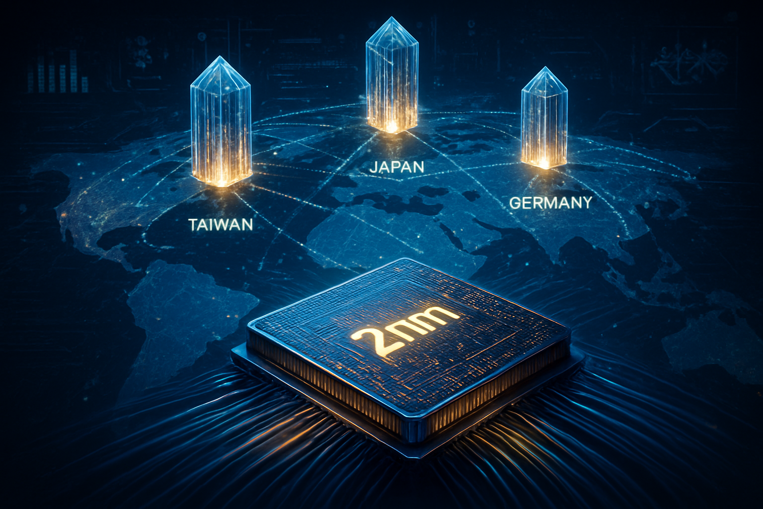
    The rise of GCT Semiconductor reflects a broader shift in market positioning. While Taiwan Semiconductor Manufacturing Company (NYSE: TSM) and Arm Holdings (NASDAQ: ARM) remain the foundational pillars of the industry, smaller, more agile players like GCT are finding strategic advantages in specific verticals. GCT’s successful reduction of its debt by nearly 50% in late 2024, combined with strategic partnerships with Samsung and Aramco Digital, has allowed it to weather the "trough of disillusionment" that followed its 2024 public listing.

    For tech giants, the success of GCT signals a growing fragmentation of the AI hardware market. Major AI labs are no longer just looking for raw compute; they are looking for specialized connectivity that can bridge the gap between centralized AI models and remote edge devices. This has created a competitive vacuum that GCT is aggressively filling. Furthermore, the disruption to existing products is evident as GCT’s 5G modules begin to replace older, less efficient 4G platforms in global markets, particularly in Saudi Arabia’s expanding 5G ecosystem.

    The strategic advantage for GCT lies in its "fabless" model, which allows it to pivot quickly to new standards like 6G research and Non-Terrestrial Networks (NTN). By integrating Iridium NTN Direct service into their chipsets, GCT has enabled seamless satellite-to-cellular connectivity—a feature that has become a major selling point for millennial investors who prioritize "future-proof" technology in their portfolios.

    The Retail Revolution 2.0: AI-Driven Investment Strategies

    The wider significance of GCT’s popularity among younger investors cannot be overstated. As of late 2025, nearly 21% of Millennials and 22% of Gen Z investors are holding AI-specific semiconductor stocks. This demographic is not just buying shares; they are using AI to do it. Retail adoption of AI-driven trading tools has surged by 46% over the last year, with platforms like Robinhood (NASDAQ: HOOD) and Webull now offering AI-curated "thematic buckets" that allow users to invest in 5G infrastructure or edge computing with a single tap.

    These AI tools perform real-time sentiment analysis, scanning social media platforms like TikTok and YouTube—where 86% of Gen Z now get their financial news—to gauge the "social buzz" around new chip launches. This "Retail Revolution 2.0" has turned semiconductor investing into a high-frequency, data-driven endeavor. For these investors, GCT Semiconductor represents the ultimate "hidden gem": a company with a low entry price (recovering from a 2025 low of $0.90) but high technical potential.

    However, this trend also raises concerns about market volatility. The "Nvidia Effect" has created a high-risk appetite among younger traders, who are three times more likely to hold speculative semiconductor stocks than Baby Boomers. While AI tools can help identify growth opportunities, they can also exacerbate "meme-stock" dynamics, where technical fundamentals are occasionally overshadowed by algorithmic social momentum.

    Future Horizons: From 5G to 6G and Pervasive AI

    Looking ahead to 2026 and beyond, the semiconductor sector is poised for further transformation. Near-term developments will likely focus on the full-scale rollout of 5G Rel 17 and the initial commercialization of 6G research. GCT Semiconductor is already laying the groundwork for this transition, with its NTN and massive IoT solutions serving as the technical foundation for future 6G standards expected by 2030.

    Potential applications on the horizon include pervasive AI, where every connected device—from smart city sensors to wearable health monitors—possesses onboard AI capabilities. Experts predict that the next challenge for the industry will be managing the energy efficiency of these billions of AI-enabled devices. GCT’s focus on low-power, high-efficiency silicon positions them well for this upcoming hurdle.

    The long-term trajectory suggests a world where connectivity and intelligence are inseparable. As AI becomes more decentralized, the demand for specialized SoCs like those produced by GCT will only increase. Analysts expect that the next two years will see a wave of consolidation in the sector, as larger tech companies look to acquire the specialized IP developed by smaller innovators.

    Conclusion: A New Era of Silicon Sovereignty

    The growing interest of millennial investors in GCT Semiconductor and the broader chip sector marks a turning point in the history of AI. We have moved past the era of "AI as a service" and into the era of "AI as infrastructure." The key takeaways from 2025 are clear: retail investors have become a sophisticated force in the market, AI tools have democratized complex technical analysis, and companies like GCT are proving that there is significant value to be found at the edge of the network.

    This development’s significance in AI history lies in the shift of focus from the "brain" (the data center) to the "nervous system" (the connectivity). As we look toward 2026, the market will be watching for GCT’s volume 5G shipments and the continued evolution of retail trading bots. For the first time, the "silicon ceiling" has been broken, allowing a new generation of investors to participate in the foundational growth of the digital age.


    This content is intended for informational purposes only and represents analysis of current AI developments.

    TokenRing AI delivers enterprise-grade solutions for multi-agent AI workflow orchestration, AI-powered development tools, and seamless remote collaboration platforms.
    For more information, visit https://www.tokenring.ai/.

  • Silicon Silk Road: India and the Netherlands Forge Strategic Alliance to Redefine Global Semiconductor Manufacturing

    Silicon Silk Road: India and the Netherlands Forge Strategic Alliance to Redefine Global Semiconductor Manufacturing

    In a move that signals a tectonic shift in the global technology landscape, India and the Netherlands have officially entered into a series of landmark agreements aimed at transforming India into a premier semiconductor powerhouse. Signed on December 19, 2025, during a high-level diplomatic visit to New Delhi, these Memoranda of Understanding (MoUs) establish a comprehensive framework for cooperation in advanced chip manufacturing, research and development, and digital security. The alliance effectively bridges the gap between Europe’s leading semiconductor equipment expertise and India’s rapidly scaling manufacturing ambitions, marking a pivotal moment in the quest for a more resilient and diversified global supply chain.

    The timing of this partnership is critical, as it coincides with the rollout of the first "Made in India" packaged semiconductor chips and the launch of the ambitious India Semiconductor Mission (ISM) 2.0. By aligning with the Netherlands—home to the world’s most advanced lithography technology—India is positioning itself not just as a consumer of technology, but as a sophisticated hub for high-end electronic hardware. This collaboration is set to accelerate India’s transition from a software-centric economy to a dual-threat powerhouse capable of designing and fabricating the hardware that powers the next generation of artificial intelligence and automotive systems.

    The core of the new alliance is the "Partnership in Semiconductors and Related Emerging Technologies," a structured framework designed to facilitate long-term cooperation in supply chain resilience. Central to this technical cooperation is the involvement of ASML (NASDAQ: ASML), the world's sole provider of Extreme Ultraviolet (EUV) lithography machines. Under the new agreements, ASML is moving beyond a sales relationship to establish specialized maintenance labs and technology-sharing initiatives within India. This is a significant technical leap, as it provides Indian fabrication units with the "holistic lithography" solutions required to produce advanced nodes, moving closer to the cutting-edge 5nm and 3nm processes essential for high-performance AI accelerators.

    In addition to hardware, the agreements include a "Joint Declaration of Intent on Enhancing Cooperation in the Digital and Cyberspace Domain." This pact focuses on the security protocols necessary for modern chip manufacturing, where digital security is as critical as physical precision. The cooperation aims to develop robust defenses against state-sponsored cyberattacks on critical digital infrastructure and to co-develop secure-by-design hardware architectures. This technical focus on "trusted hardware" distinguishes the Indo-Dutch partnership from previous bilateral agreements, which often focused solely on trade volume rather than the fundamental security of the silicon itself.

    Industry experts have reacted with notable optimism, highlighting that the "Indo-Dutch Semiconductor Partnership for Talent" is perhaps the most technically significant long-term component. The initiative aims to train 85,000 semiconductor professionals over the next five years through direct institutional linkages between the Indian Institutes of Technology (IITs) and Dutch technical universities. This massive infusion of specialized human capital is intended to address the global talent shortage in VLSI (Very Large Scale Integration) design and advanced wafer fabrication, providing the technical backbone for India's burgeoning fab ecosystem.

    The implications for the corporate sector are profound, with several tech giants already positioning themselves to capitalize on the new framework. NXP Semiconductors (NASDAQ: NXPI) has announced a massive $1 billion expansion in India, including the acquisition of land for a second R&D hub in the Greater Noida Semiconductor Park. This facility will focus specifically on 5nm automotive chips and AI-integrated hardware, aiming to double NXP's Indian engineering workforce to over 6,000 by 2026. For NXP, the MoU provides a stable regulatory environment and a direct pipeline to the emerging Indian EV market, which is hungry for high-end silicon.

    For major AI labs and tech companies, this development offers a critical alternative to the current manufacturing concentration in East Asia. Companies like Micron Technology (NASDAQ: MU) are already seeing the benefits of India's aggressive policy push; Micron’s Sanand plant is among the first to roll out packaged chips this month. The entry of Dutch expertise into the Indian market creates a competitive environment that challenges the dominance of established hubs. This shift is likely to disrupt existing product timelines as companies begin to integrate "India-sourced" components into their global portfolios to mitigate geopolitical risks.

    Furthermore, Indian conglomerates are stepping up to the plate. Tata Electronics, a subsidiary of the Tata Group—which includes publicly traded entities like Tata Motors (NYSE: TTM)—is heavily invested in building out OSAT (Outsourced Semiconductor Assembly and Test) facilities and full-scale fabs. The partnership with the Netherlands provides these domestic players with a shortcut to world-class manufacturing standards. By leveraging Dutch lithography and security expertise, Indian firms can offer global tech giants a "China+1" manufacturing strategy that does not sacrifice technical sophistication for geographic diversity.

    The broader significance of this alliance cannot be overstated. It represents the formalization of the "Silicon Silk Road," a strategic trade corridor that connects European high-tech equipment with Indian industrial scale. In the current global landscape, where semiconductor sovereignty has become a matter of national security, this partnership serves as a blueprint for middle-power collaboration. It fits into a wider trend of "friend-shoring," where democratic nations align their supply chains to ensure that the hardware powering AI and critical infrastructure is built within a trusted ecosystem.

    However, the rapid expansion of India's semiconductor footprint is not without its concerns. Critics point to the immense environmental cost of chip manufacturing, particularly regarding water consumption and chemical waste. As India scales its production, the challenge will be to implement the "green manufacturing" standards that the Netherlands has pioneered. Furthermore, the global semiconductor market is notoriously cyclical; by the time India’s major fabs are fully operational in the late 2020s, the industry may face a different set of oversupply or demand challenges compared to the shortages of the early 2020s.

    When compared to previous milestones, such as the initial launch of the India Semiconductor Mission in 2021, the 2025 MoUs represent a shift from aspiration to execution. While the first phase of ISM focused on attracting investment, "ISM 2.0"—with its proposed $20 billion outlay—is focused on advanced nodes and specialized materials like Silicon Carbide (SiC). This evolution mirrors the trajectory of other successful semiconductor hubs, but at a significantly accelerated pace, driven by the urgent global need for supply chain resilience.

    Looking ahead, the next 24 to 36 months will be a period of intense construction and calibration. The near-term focus will be on the successful rollout of commercial-grade chips from the 10 major approved projects currently underway across states like Gujarat, Assam, and Uttar Pradesh. We can expect to see the first Indian-made AI accelerators and automotive sensors hitting the market by 2027. These will likely find immediate use cases in India's massive domestic automotive sector and its burgeoning fleet of AI-powered public service platforms.

    The long-term challenge remains the development of a self-sustaining R&D ecosystem. While the MoUs provide the framework for talent development, the ultimate goal is for India to move from "assembling and testing" to "innovating and leading." Experts predict that the next frontier for the Indo-Dutch partnership will be in the realm of Quantum Computing and Photonic chips, where the Netherlands already holds a significant lead. If India can successfully integrate these future-gen technologies into its manufacturing roadmap, it could leapfrog traditional silicon technologies entirely.

    The signing of the India-Netherlands MoUs on December 19, 2025, marks a definitive chapter in the history of the semiconductor industry. By combining Dutch technical mastery in lithography and digital security with India's massive scale, talent pool, and government backing, the two nations have created a formidable alliance. The key takeaways are clear: India is no longer just a potential player in the chip game; it is an active, strategic hub that is successfully attracting the world's most sophisticated technology partners.

    This development will be remembered as the moment when the global semiconductor map was permanently redrawn. The immediate significance lies in the diversification of the supply chain, but the long-term impact will be felt in the democratization of high-tech manufacturing. In the coming weeks and months, the industry will be watching for the formal approval of ISM 2.0 and the first performance benchmarks of the chips rolling out from Indian facilities. For the global tech industry, the message is clear: the future of silicon is increasingly taking root in Indian soil.


    This content is intended for informational purposes only and represents analysis of current AI and semiconductor developments as of December 19, 2025.

    TokenRing AI delivers enterprise-grade solutions for multi-agent AI workflow orchestration, AI-powered development tools, and seamless remote collaboration platforms. For more information, visit https://www.tokenring.ai/.

  • The Silicon Architect: How Lam Research’s AI-Driven 127% Surge Defined the 2025 Semiconductor Landscape

    The Silicon Architect: How Lam Research’s AI-Driven 127% Surge Defined the 2025 Semiconductor Landscape

    As 2025 draws to a close, the semiconductor industry is reflecting on a year of unprecedented growth, and no company has captured the market's imagination—or capital—quite like Lam Research (NASDAQ: LRCX). With a staggering 127% year-to-date surge as of December 19, 2025, the California-based equipment giant has officially transitioned from a cyclical hardware supplier to the primary architect of the AI infrastructure era. This rally, which has seen Lam Research significantly outperform its primary rival Applied Materials (NASDAQ: AMAT), marks a historic shift in how Wall Street values the "picks and shovels" of the artificial intelligence boom.

    The significance of this surge lies in Lam's specialized dominance over the most critical bottlenecks in AI chip production: High Bandwidth Memory (HBM) and next-generation transistor architectures. As the industry grapples with the "memory wall"—the growing performance gap between fast processors and slower memory—Lam Research has positioned itself as the indispensable provider of the etching and deposition tools required to build the complex 3D structures that define modern AI hardware.

    Engineering the 2nm Era: The Akara and Cryo Breakthroughs

    The technical backbone of Lam’s 2025 performance is a suite of revolutionary tools that have redefined precision at the atomic scale. At the forefront is the Lam Cryo™ 3.0, a cryogenic etching platform that operates at -80°C. This technology has become the industry standard for producing Through-Silicon Vias (TSVs) in HBM4 memory. By utilizing ultra-low temperatures, the tool achieves vertical etch profiles at 2.5 times the speed of traditional methods, a capability that has been hailed by the research community as the "holy grail" for mass-producing the dense memory stacks required for NVIDIA (NASDAQ: NVDA) and AMD (NASDAQ: AMD) accelerators.

    Further driving this growth is the Akara® Conductor Etch platform, the industry’s first solid-state plasma source etcher. Introduced in early 2025, Akara provides the sub-angstrom precision necessary for shaping Gate-All-Around (GAA) transistors, which are replacing the aging FinFET architecture as the industry moves toward 2nm and 1.8nm nodes. With 100 times faster responsiveness than previous generations, Akara has allowed Lam to capture an estimated 80% market share in the sub-3nm etch segment. Additionally, the company’s introduction of ALTUS® Halo, a tool capable of mass-producing Molybdenum layers to replace Tungsten, has been described as a paradigm shift. Molybdenum reduces electrical resistance by over 50%, enabling the power-efficient scaling that is mandatory for the next generation of data center CPUs and GPUs.

    A Competitive Re-Alignment in the WFE Market

    Lam Research’s 127% rise has sent ripples through the Wafer Fabrication Equipment (WFE) market, forcing competitors and customers to re-evaluate their strategic positions. While Applied Materials remains a powerhouse in materials engineering, Lam’s concentrated focus on "etch-heavy" processes has given it a distinct advantage as chips become increasingly three-dimensional. In 2025, Lam’s gross margins consistently exceeded the 50% threshold for the first time in over a decade, a feat attributed to its high-value proprietary technology in the HBM and GAA sectors.

    This dominance has created a symbiotic relationship with leading chipmakers like Taiwan Semiconductor Manufacturing Company (NYSE: TSM), Samsung Electronics (KRX: 005930), and SK Hynix (KRX: 000660). As these giants race to build the world’s first 1.8nm production lines, they have become increasingly dependent on Lam’s specialized tools. For startups and smaller AI labs, the high cost of this equipment has further raised the barrier to entry for custom silicon, reinforcing the dominance of established tech giants who can afford the billions in capital expenditure required to outfit a modern fab with Lam’s latest platforms.

    The Silicon Renaissance and the End of the "Memory Wall"

    The broader significance of Lam’s 2025 performance cannot be overstated. It signals the arrival of the "Silicon Renaissance," where the focus of AI development has shifted from software algorithms to the physical limitations of hardware. For years, the industry feared a stagnation in Moore’s Law, but Lam’s breakthroughs in 3D stacking and materials science have provided a new roadmap for growth. By solving the "memory wall" through advanced HBM4 production tools, Lam has effectively extended the runway for the entire AI industry.

    However, this growth has not been without its complexities. The year 2025 also saw a significant recalibration of the global supply chain. Lam Research’s revenue exposure to China, which peaked at over 40% in previous years, began to shift as U.S. export controls tightened. This geopolitical friction has been offset by the massive influx of investment driven by the U.S. CHIPS Act. As Lam navigates these regulatory waters, its performance serves as a barometer for the broader "tech cold war," where control over semiconductor manufacturing equipment is increasingly viewed as a matter of national security.

    Looking Toward 2026: The $1 Trillion Milestone

    Heading into 2026, the outlook for Lam Research remains bullish, though tempered by potential cyclical normalization. Analysts at major firms like Goldman Sachs (NYSE: GS) and JPMorgan (NYSE: JPM) have set price targets ranging from $160 to $200, citing the continued "wafer intensity" of AI chips. The industry is currently on a trajectory to reach $1 trillion in total semiconductor revenue by 2030, and 2026 is expected to be a pivotal year as the first 2nm-capable fabs in the United States, including TSMC’s Arizona Fab 2 and Intel’s (NASDAQ: INTC) Ohio facilities, begin their major equipment move-in phases.

    The near-term focus will be on the ramp-up of Backside Power Delivery, a new chip architecture that moves power routing to the bottom of the wafer to improve efficiency. Lam is expected to be a primary beneficiary of this transition, as it requires specialized etching steps that play directly into the company’s core strengths. Challenges remain, particularly regarding the potential for "digestion" in the NAND market if capacity overshoots demand, but the structural need for AI-optimized memory suggests that any downturn may be shallower than in previous cycles.

    A Historic Year for AI Infrastructure

    In summary, Lam Research’s 127% surge in 2025 is more than just a stock market success story; it is a testament to the critical role of materials science in the AI revolution. By mastering the atomic-level manipulation of silicon and new materials like Molybdenum, Lam has become the gatekeeper of the next generation of computing. The company’s ability to innovate at the physical limits of nature has allowed it to outperform the broader market and cement its place as a cornerstone of the global technology ecosystem.

    As we move into 2026, investors and industry observers should watch for the continued expansion of domestic manufacturing in the U.S. and Europe, as well as the initial production yields of 1.8nm chips. While geopolitical tensions and cyclical risks persist, Lam Research has proven that in the gold rush of artificial intelligence, the most valuable players are those providing the tools to dig deeper, stack higher, and process faster than ever before.


    This content is intended for informational purposes only and represents analysis of current AI developments.

    TokenRing AI delivers enterprise-grade solutions for multi-agent AI workflow orchestration, AI-powered development tools, and seamless remote collaboration platforms.
    For more information, visit https://www.tokenring.ai/.

  • The Backbone of Intelligence: Micron’s Q1 Surge Signals No End to the AI Memory Supercycle

    The Backbone of Intelligence: Micron’s Q1 Surge Signals No End to the AI Memory Supercycle

    The artificial intelligence revolution has found its latest champion not in the form of a new large language model, but in the silicon architecture that feeds them. Micron Technology (NASDAQ: MU) reported its fiscal first-quarter 2026 earnings on December 17, 2025, delivering a performance that shattered Wall Street expectations and underscored a fundamental shift in the tech landscape. The company’s revenue soared to $13.64 billion—a staggering 57% year-over-year increase—driven almost entirely by the insatiable demand for High Bandwidth Memory (HBM) in AI data centers.

    This "earnings beat" is more than just a financial milestone; it is a signal that the "AI Memory Supercycle" is entering a new, more aggressive phase. Micron CEO Sanjay Mehrotra revealed that the company’s entire HBM production capacity is effectively sold out through the end of the 2026 calendar year. As AI models grow in complexity, the industry’s focus has shifted from raw processing power to the "memory wall"—the critical bottleneck where data transfer speeds cannot keep pace with GPU calculations. Micron’s results suggest that for the foreseeable future, the companies that control the memory will control the pace of AI development.

    The Technical Frontier: HBM3E and the HBM4 Roadmap

    At the heart of Micron’s dominance is its leadership in HBM3E (High Bandwidth Memory 3 Extended), which is currently in high-volume production. Unlike traditional DRAM, HBM stacks memory chips vertically, utilizing Through-Silicon Vias (TSVs) to create a massive data highway directly adjacent to the AI processor. Micron’s HBM3E has gained significant traction because it is roughly 30% more power-efficient than competing offerings from rivals like SK Hynix (KRX: 000660). In an era where data center power consumption is a primary constraint for hyperscalers, this efficiency is a major competitive advantage.

    Looking ahead, the technical specifications for the next generation, HBM4, are already defining the 2026 roadmap. Micron plans to begin sampling HBM4 by mid-2026, with a full production ramp scheduled for the second quarter of that year. These new modules are expected to feature industry-leading speeds exceeding 11 Gbps and move toward a 12-layer and 16-layer stacking architecture. This transition is technically challenging, requiring precision at the nanometer scale to manage heat dissipation and signal integrity across the vertical stacks.

    The AI research community has noted that the shift to HBM4 will likely involve a move toward "custom HBM," where the base logic die of the memory stack is manufactured on advanced logic processes (like TSMC’s 5nm or 3nm). This differs significantly from previous approaches where memory was a standardized commodity. By integrating more logic directly into the memory stack, Micron and its partners aim to reduce latency even further, effectively blurring the line between where "thinking" happens and where "memory" resides.

    Market Dynamics: A Three-Way Battle for Supremacy

    Micron’s stellar quarter has profound implications for the competitive landscape of the semiconductor industry. While SK Hynix remains the market leader with approximately 62% of the HBM market share, Micron has solidified its second-place position at 21%, successfully leapfrogging Samsung (KRX: 005930), which currently holds 17%. The market is no longer a race to the bottom on price, but a race to the top on yield and reliability. Micron’s decision in late 2025 to exit its "Crucial" consumer-facing business to focus exclusively on AI and data center products highlights the strategic pivot toward high-margin enterprise silicon.

    The primary beneficiaries of Micron’s success are the GPU giants, Nvidia (NASDAQ: NVDA) and Advanced Micro Devices (NASDAQ: AMD). Micron is a critical supplier for Nvidia’s Blackwell (GB200) architecture and the upcoming Vera Rubin platform. For AMD, Micron’s HBM3E is a vital component of the Instinct MI350 accelerators. However, the "sold out" status of these memory chips creates a strategic dilemma: major AI labs and cloud providers are now competing not just for GPUs, but for the memory allocated to those GPUs. This scarcity gives Micron immense pricing power, reflected in its gross margin expansion to 56.8%.

    The competitive pressure is forcing rivals to take drastic measures. Samsung has recently announced a partnership with TSMC for HBM4 packaging, an unprecedented move for the vertically integrated giant, in an attempt to regain its footing. Meanwhile, the tight supply has turned memory into a geopolitical asset. Micron’s expansion of manufacturing facilities in Idaho and New York, supported by the CHIPS Act, provides a "Western" supply chain alternative that is increasingly attractive to U.S.-based tech giants looking to de-risk their infrastructure from East Asian dependencies.

    The Wider Significance: Breaking the Memory Wall

    The AI memory boom represents a pivot point in the history of computing. For decades, the industry followed Moore’s Law, focusing on doubling transistor density. But the rise of Generative AI has exposed the "Memory Wall"—the reality that even the fastest processors are useless if they are "starved" for data. This has elevated memory from a background commodity to a strategic infrastructure component on par with the processors themselves. Analysts now describe Micron’s revenue potential as "second only to Nvidia" in the AI ecosystem.

    However, this boom is not without concerns. The massive capital expenditure required to stay competitive—Micron raised its FY2026 CapEx to $20 billion—creates a high-stakes environment where any yield issue or technological delay could be catastrophic. Furthermore, the energy consumption of these high-performance memory stacks is contributing to the broader environmental challenge of AI. While Micron’s 30% efficiency gain is a step in the right direction, the sheer scale of the projected $100 billion HBM market by 2028 suggests that memory will remain a significant portion of the global data center power footprint.

    Comparing this to previous milestones, such as the mobile internet explosion or the shift to cloud computing, the AI memory surge is unique in its velocity. We are seeing a total restructuring of how hardware is designed. The "Memory-First" architecture is becoming the standard for the next generation of supercomputers, moving away from the von Neumann architecture that has dominated computing for over half a century.

    Future Horizons: Custom Silicon and the Vera Rubin Era

    As we look toward 2026 and beyond, the integration of memory and logic will only deepen. The upcoming Nvidia Vera Rubin platform, expected in the second half of 2026, is being designed from the ground up to utilize HBM4. This will likely enable models with tens of trillions of parameters to run with significantly lower latency. We can also expect to see the rise of CXL (Compute Express Link) technologies, which will allow for memory pooling across entire data center racks, further breaking down the barriers between individual servers.

    The next major challenge for Micron and its peers will be the transition to "hybrid bonding" for HBM4 and HBM5. This technique eliminates the need for traditional solder bumps between chips, allowing for even denser stacks and better thermal performance. Experts predict that the first company to master hybrid bonding at scale will likely capture the lion’s share of the HBM4 market, as it will be essential for the 16-layer stacks required by the next generation of AI training clusters.

    Conclusion: A New Era of Hardware-Software Co-Design

    Micron’s Q1 FY2026 earnings report is a watershed moment that confirms the AI memory boom is a structural shift, not a temporary spike. By exceeding revenue targets and selling out capacity through 2026, Micron has proven that memory is the indispensable fuel of the AI era. The company’s strategic pivot toward high-efficiency HBM and its aggressive roadmap for HBM4 position it as a foundational pillar of the global AI infrastructure.

    In the coming weeks and months, investors and industry watchers should keep a close eye on the HBM4 sampling process and the progress of Micron’s U.S.-based fabrication plants. As the "Memory Wall" continues to be the defining challenge of AI scaling, the collaboration between memory makers like Micron and logic designers like Nvidia will become the most critical relationship in technology. The era of the commodity memory chip is over; the era of the intelligent, high-bandwidth foundation has begun.


    This content is intended for informational purposes only and represents analysis of current AI developments.

    TokenRing AI delivers enterprise-grade solutions for multi-agent AI workflow orchestration, AI-powered development tools, and seamless remote collaboration platforms.
    For more information, visit https://www.tokenring.ai/.

  • The Green Paradox: Can the AI Boom Survive the Semiconductor Industry’s Rising Resource Demands?

    The Green Paradox: Can the AI Boom Survive the Semiconductor Industry’s Rising Resource Demands?

    As of December 19, 2025, the global technology sector is grappling with a profound "green paradox." While artificial intelligence is being hailed as a critical tool for solving climate change, the physical manufacturing of the chips that power it—such as Nvidia’s Blackwell and Blackwell Ultra architectures—has pushed the semiconductor industry’s energy and water consumption to unprecedented levels. This week, industry leaders and environmental regulators have signaled a major pivot toward "Sustainable Silicon," as the resource-heavy requirements of 3nm and 2nm fabrication nodes begin to clash with global net-zero commitments.

    The immediate significance of this shift cannot be overstated. With the AI chip market continuing its meteoric rise, the environmental footprint of a single leading-edge wafer has nearly tripled compared to a decade ago. This has forced the world's largest chipmakers to adopt radical new technologies, from AI-driven "Digital Twin" factories to closed-loop water recycling systems, in an effort to decouple industrial growth from environmental degradation.

    Engineering the Closed-Loop Fab: Technical Breakthroughs in 2025

    The technical challenge of modern chip fabrication lies in the extreme complexity of the latest manufacturing nodes. As companies like TSMC (NYSE: TSM) and Samsung (KRX: 005930) move toward 2nm production, the number of mask layers and chemical processing steps has increased significantly. To combat the resulting resource drain, the industry has turned to "Counterflow Reverse Osmosis," a breakthrough in Ultra Pure Water (UPW) management. This technology now allows fabs to recycle up to 90% of their wastewater directly back into the sensitive wafer-rinsing stages—a feat previously thought impossible due to the risk of microscopic contamination.

    Energy consumption remains the industry's largest hurdle, primarily driven by Extreme Ultraviolet (EUV) lithography tools manufactured by ASML (NASDAQ: ASML). These machines, which are essential for printing the world's most advanced transistors, consume roughly 1.4 megawatts of power each. To mitigate this, TSMC has fully deployed its "EUV Dynamic Power Saving" program this year. By using real-time AI to pulse the EUV light source only when necessary, the system has successfully reduced tool-level energy consumption by 8% without sacrificing throughput.

    Furthermore, the industry is seeing a surge in AI-driven yield optimization. By utilizing deep learning for defect detection, manufacturers have reported a 40% reduction in defect rates on 3nm lines. This efficiency is a sustainability win: by catching errors early, fabs prevent the "waste" of thousands of gallons of UPW and hundreds of kilowatts of energy that would otherwise be spent processing a defective wafer. Industry experts have praised these advancements, noting that the "Intelligence-to-Efficiency" loop is finally closing, where AI chips are being used to optimize the very factories that produce them.

    The Competitive Landscape: Tech Giants Race for 'Green' Dominance

    The push for sustainability is rapidly becoming a competitive differentiator for the world's leading foundries and integrated device manufacturers. Intel (NASDAQ: INTC) has emerged as an early leader in renewable energy adoption, announcing this month that it has achieved 98% global renewable electricity usage. Intel’s "Net Positive Water" goal is also ahead of schedule, with its facilities in the United States and India already restoring more water to local ecosystems than they consume. This positioning is a strategic advantage as cloud providers seek to lower their Scope 3 emissions.

    For Nvidia (NASDAQ: NVDA), the sustainability of the fabrication process is now a core component of its market positioning. As the primary customer for TSMC’s most advanced nodes, Nvidia is under pressure from its own enterprise clients to provide "Green AI" solutions. The massive die size of Nvidia's Blackwell GPUs means fewer chips can be harvested from a single wafer, making each chip more "resource-expensive" than a standard mobile processor. In response, Nvidia has partnered with Samsung to develop Digital Twins of entire fabrication plants, using over 50,000 GPUs to simulate and optimize airflow and power loads, improving overall operational efficiency by an estimated 20%.

    This shift is also disrupting the supply chain for equipment manufacturers like Applied Materials (NASDAQ: AMAT) and Lam Research (NASDAQ: LRCX). There is a growing demand for "dry" lithography and etching solutions that eliminate the need for water-intensive processes. Startups focusing on sustainable chemistry are also finding new opportunities as the industry moves away from "forever chemicals" (PFAS) in response to tightening global regulations.

    The Regulatory Hammer and the Broader AI Landscape

    The broader significance of these developments is underscored by a new wave of international regulations. As of November 2024, the Global Electronics Council introduced stricter EPEAT criteria for semiconductors, and in 2025, the European Union's "Digital Product Passport" (DPP) became a mandatory requirement for chips sold in the region. This regulation forces manufacturers to provide a transparent "cradle-to-gate" account of the carbon and water footprint for every chip, effectively making sustainability a prerequisite for market access in Europe.

    This regulatory environment marks a departure from previous AI milestones, where the focus was almost entirely on performance and "flops per watt." Today, the conversation has shifted to the "embedded" environmental cost of the hardware itself. Concerns are mounting that the resource intensity of AI could lead to localized water shortages or energy grid instability in semiconductor hubs like Arizona, Taiwan, and South Korea. This has led to a comparison with the early days of data center expansion, but at a much more concentrated and resource-intensive scale.

    The Semiconductor Climate Consortium (SCC) has also launched a standardized Scope 3 reporting framework this year. This compels fabs to account for the carbon footprint of their entire supply chain, from raw silicon mining to the production of specialty gases. By standardizing these metrics, the industry is moving toward a future where "green silicon" could eventually command a price premium over traditionally manufactured chips.

    Looking Ahead: The Road to 2nm and Circularity

    In the near term, the industry is bracing for the transition to 2nm nodes, which is expected to begin in earnest in late 2026. While these nodes promise greater energy efficiency for the end-user, the fabrication process will be the most resource-intensive in history. Experts predict that the next major breakthrough will involve a move toward a "circular economy" for semiconductors, where rare-earth metals and silicon are reclaimed from decommissioned AI servers and fed back into the manufacturing loop.

    Potential applications on the horizon include the integration of small-scale modular nuclear reactors (SMRs) directly into fab campuses to provide a stable, carbon-free baseload of energy. Challenges remain, particularly in the elimination of PFAS, as many of the chemical substitutes currently under testing have yet to match the precision required for leading-edge nodes. However, the trajectory is clear: the semiconductor industry is moving toward a "Zero-Waste" model that treats water and energy as finite, precious resources rather than cheap industrial inputs.

    A New Era for Sustainable Computing

    The push for sustainability in semiconductor manufacturing represents a pivotal moment in the history of computing. The key takeaway from 2025 is that the AI revolution cannot be sustained by 20th-century industrial practices. The industry’s ability to innovate its way out of the "green paradox"—using AI to optimize the fabrication of AI—will determine the long-term viability of the current technological boom.

    As we look toward 2026, the industry's success will be measured not just by transistor density or clock speeds, but by gallons of water saved and carbon tons avoided. The shift toward transparent reporting and closed-loop manufacturing is a necessary evolution for a sector that has become the backbone of the global economy. Investors and consumers alike should watch for the first "Water-Positive" fab certifications and the potential for a "Green Silicon" labeling system to emerge in the coming months.


    This content is intended for informational purposes only and represents analysis of current AI developments.

    TokenRing AI delivers enterprise-grade solutions for multi-agent AI workflow orchestration, AI-powered development tools, and seamless remote collaboration platforms.
    For more information, visit https://www.tokenring.ai/.

  • The Intelligence Revolution Moves Inward: How Edge AI Silicon is Reclaiming Privacy and Performance

    The Intelligence Revolution Moves Inward: How Edge AI Silicon is Reclaiming Privacy and Performance

    As we close out 2025, the center of gravity for artificial intelligence has undergone a seismic shift. For years, the narrative of AI progress was defined by massive, power-hungry data centers and the "cloud-first" approach that required every query to travel hundreds of miles to a server rack. However, the final quarter of 2025 has solidified a new era: the era of Edge AI. Driven by a new generation of specialized semiconductors, high-performance AI is no longer a remote service—it is a local utility living inside our smartphones, IoT sensors, and wearable devices.

    This transition represents more than just a technical milestone; it is a fundamental restructuring of the digital ecosystem. By moving the "brain" of the AI directly onto the device, manufacturers are solving the three greatest hurdles of the generative AI era: latency, privacy, and cost. With the recent launches of flagship silicon from industry titans and a regulatory environment increasingly favoring "privacy-by-design," the rise of Edge AI silicon is the defining tech story of the year.

    The Architecture of Autonomy: Inside the 2025 Silicon Breakthroughs

    The technical landscape of late 2025 is dominated by a new class of Neural Processing Units (NPUs) that have finally bridged the gap between mobile efficiency and server-grade performance. At the heart of this revolution is the Apple Inc. (NASDAQ: AAPL) A19 Pro chip, which debuted in the iPhone 17 Pro this past September. Unlike previous iterations, the A19 Pro features a 16-core Neural Engine and, for the first time, integrated neural accelerators within the GPU cores themselves. This "hybrid compute" architecture allows the device to run 8-billion-parameter models like Llama-3 with sub-second response times, enabling real-time "Visual Intelligence" that can analyze everything the camera sees without ever uploading a single frame to the cloud.

    Not to be outdone, Qualcomm Inc. (NASDAQ: QCOM) recently unveiled the Snapdragon 8 Elite Gen 5, a powerhouse that delivers an unprecedented 80 TOPS (Tera Operations Per Second) of AI performance. The chip’s second-generation Oryon CPU cores are specifically optimized for "agentic AI"—software that doesn't just answer questions but performs multi-step tasks across different apps locally. Meanwhile, MediaTek Inc. (TPE: 2454) has disrupted the mid-range market with its Dimensity 9500, the first mobile SoC to natively support BitNet 1.58-bit (ternary) model processing. This mathematical breakthrough allows for a 40% acceleration in model loading while reducing power consumption by a third, making high-end AI accessible on more affordable hardware.

    These advancements differ from previous approaches by moving away from general-purpose computing toward "Physical AI." While older chips treated AI as a secondary task, 2025’s silicon is built from the ground up to handle transformer-based networks and vision-language models (VLMs). Initial reactions from the research community, including experts at the AI Infra Summit in Santa Clara, suggest that the "pre-fill" speeds—the time it takes for an AI to understand a prompt—have improved by nearly 300% year-over-year, effectively killing the "loading" spinner that once plagued mobile AI.

    Strategic Realignment: The Battle for the Edge

    The rise of specialized Edge silicon is forcing a massive strategic pivot among tech giants. For NVIDIA Corporation (NASDAQ: NVDA), the focus has expanded from the data center to the "personal supercomputer." Their new Project Digits platform, powered by the Blackwell-based GB10 Grace Blackwell Superchip, allows developers to run 200-billion-parameter models locally. By providing the hardware for "Sovereign AI," NVIDIA is positioning itself as the infrastructure provider for enterprises that are too privacy-conscious to use public clouds.

    The competitive implications are stark. Traditional cloud providers like Alphabet Inc. (NASDAQ: GOOGL) and Microsoft Corporation (NASDAQ: MSFT) are now in a race to vertically integrate. Google’s Tensor G5, manufactured by Taiwan Semiconductor Manufacturing Company (NYSE: TSM) on its refined 3nm process, is a direct attempt to decouple Pixel's AI features from the Google Cloud, ensuring that Gemini Nano can function in "Airplane Mode." This shift threatens the traditional SaaS (Software as a Service) model; if the device in your pocket can handle the compute, the need for expensive monthly AI subscriptions may begin to evaporate, forcing companies to find new ways to monetize the "intelligence" they provide.

    Startups are also finding fertile ground in this new hardware reality. Companies like Hailo and Tenstorrent (led by legendary architect Jim Keller) are licensing RISC-V based AI IP, allowing niche manufacturers to build custom silicon for everything from smart mirrors to industrial robots. This democratization of high-performance silicon is breaking the duopoly of ARM and x86, leading to a more fragmented but highly specialized hardware market.

    Privacy, Policy, and the Death of Latency

    The broader significance of Edge AI lies in its ability to resolve the "Privacy Paradox." Until now, users had to choose between the power of large-scale AI and the security of their personal data. With the 2025 shift, "Local RAG" (Retrieval-Augmented Generation) has become the standard. This allows a device to index a user’s entire digital life—emails, photos, and health data—locally, providing a hyper-personalized AI experience that never leaves the device.

    This hardware-led privacy has caught the eye of regulators. On December 11, 2025, the US administration issued a landmark Executive Order on National AI Policy, which explicitly encourages "privacy-by-design" through on-device processing. Similarly, the European Union's recent "Digital Omnibus" package has shown a willingness to loosen certain data-sharing restrictions for companies that utilize local inference, recognizing it as a superior method for protecting citizen data. This alignment of hardware capability and government policy is accelerating the adoption of AI in sensitive sectors like healthcare and defense.

    Comparatively, this milestone is being viewed as the "Broadband Moment" for AI. Just as the transition from dial-up to broadband enabled the modern web, the transition from cloud-AI to Edge-AI is enabling "ambient intelligence." We are moving away from a world where we "use" AI to a world where AI is a constant, invisible layer of our physical environment, operating with sub-50ms latency that feels instantaneous to the human brain.

    The Horizon: From Smartphones to Humanoids

    Looking ahead to 2026, the trajectory of Edge AI silicon points toward even deeper integration into the physical world. We are already seeing the first wave of "AI-enabled sensors" from Sony Group Corporation (NYSE: SONY) and STMicroelectronics N.V. (NYSE: STM). These sensors don't just capture images or motion; they perform inference within the sensor housing itself, outputting only metadata. This "intelligence at the source" will be critical for the next generation of AR glasses, which require extreme power efficiency to maintain a lightweight form factor.

    Furthermore, the "Physical AI" tier is set to explode. NVIDIA's Jetson AGX Thor, designed for humanoid robots, is now entering mass production. Experts predict that the lessons learned from mobile NPU efficiency will directly translate to more capable, longer-lasting autonomous robots. The challenge remains in the "memory wall"—the difficulty of moving data fast enough between memory and the processor—but advancements in HBM4 (High Bandwidth Memory) and analog-in-memory computing from startups like Syntiant are expected to address these bottlenecks by late 2026.

    A New Chapter in the Silicon Sagas

    The rise of Edge AI silicon in 2025 marks the end of the "Cloud-Only" era of artificial intelligence. By successfully shrinking the immense power of LLMs into pocket-sized form factors, the semiconductor industry has delivered on the promise of truly personal, private, and portable intelligence. The key takeaways are clear: hardware is once again the primary driver of software innovation, and privacy is becoming a feature of the silicon itself, rather than just a policy on a website.

    As we move into 2026, the industry will be watching for the first "Edge-native" applications that can do things cloud AI never could—such as real-time, offline translation of complex technical jargon or autonomous drone navigation in GPS-denied environments. The intelligence revolution has moved inward, and the devices we carry are no longer just windows into a digital world; they are the architects of it.


    This content is intended for informational purposes only and represents analysis of current AI developments.

    TokenRing AI delivers enterprise-grade solutions for multi-agent AI workflow orchestration, AI-powered development tools, and seamless remote collaboration platforms.
    For more information, visit https://www.tokenring.ai/.

  • Silicon Diplomacy: How TSMC’s Global Triad is Redrawing the Map of AI Power

    Silicon Diplomacy: How TSMC’s Global Triad is Redrawing the Map of AI Power

    As of December 19, 2025, the global semiconductor landscape has undergone its most radical transformation since the invention of the integrated circuit. Taiwan Semiconductor Manufacturing Company (NYSE:TSM), long the sole guardian of the world’s most advanced "Silicon Shield," has successfully metastasized into a global triad of manufacturing power. With its massive facilities in Arizona, Japan, and Germany now either fully operational or nearing completion, the company has effectively decentralized the production of the world’s most critical resource: the high-performance AI chips that fuel everything from generative large language models to autonomous defense systems.

    This expansion marks a pivot from "efficiency-first" to "resilience-first" economics. The immediate significance of TSMC’s international footprint is twofold: it provides a geographical hedge against geopolitical tensions in the Taiwan Strait and creates a localized supply chain for the world's most valuable tech giants. By late 2025, the "Made in USA" and "Made in Japan" labels on high-end silicon are no longer aspirations—they are a reality that is fundamentally reshaping how AI companies calculate risk and roadmap their future hardware.

    The Yield Surprise: Arizona and the New Technical Standard

    The most significant technical milestone of 2025 has been the performance of TSMC’s Fab 1 in Phoenix, Arizona. Initially plagued by labor disputes and cultural friction during its construction phase, the facility has silenced critics by achieving 4nm and 5nm yield rates that are approximately 4 percentage points higher than equivalent fabs in Taiwan, reaching a staggering 92%. This technical feat is largely attributed to the implementation of "Digital Twin" manufacturing technology, where every process in the Arizona fab is mirrored and optimized in a virtual environment before execution, combined with a highly automated workforce model that mitigated early staffing challenges.

    While Arizona focuses on the cutting-edge 4nm and 3nm nodes (with 2nm production accelerated for 2027), the Japanese and German expansions serve different but equally vital technical roles. In Kumamoto, Japan, the JASM (Japan Advanced Semiconductor Manufacturing) facility has successfully ramped up 12nm to 28nm production, providing the specialized logic required for image sensors and automotive AI. Meanwhile, the ESMC (European Semiconductor Manufacturing Company) in Dresden, Germany, has broken ground on a facility dedicated to 16nm and 28nm "specialty" nodes. These are not the flashy chips that power ChatGPT, but they are the essential "glue" for the industrial and automotive AI sectors that keep Europe’s economy moving.

    Perhaps the most critical technical development of late 2025 is the expansion of advanced packaging. AI chips like NVIDIA’s (NASDAQ:NVDA) Blackwell and upcoming Rubin platforms rely on CoWoS (Chip-on-Wafer-on-Substrate) packaging to function. To support its international fabs, TSMC has entered a landmark partnership with Amkor Technology (NASDAQ:AMKR) in Peoria, Arizona, to provide "turnkey" advanced packaging services. This ensures that a chip can be fabricated, packaged, and tested entirely on U.S. soil—a first for the high-end AI industry.

    Initial reactions from the AI research and engineering communities have been overwhelmingly positive. Hardware architects at major labs note that the proximity of these fabs to U.S.-based design centers allows for faster "tape-out" cycles and reduced latency in the prototyping phase. The technical success of the Arizona site, in particular, has validated the theory that leading-edge manufacturing can indeed be successfully exported from Taiwan if supported by sufficient capital and automation.

    The AI Titans and the "US-Made" Premium

    The primary beneficiaries of TSMC’s global expansion are the "Big Three" of AI hardware: Apple (NASDAQ:AAPL), NVIDIA, and AMD (NASDAQ:AMD). For these companies, the international fabs represent more than just extra capacity; they offer a strategic advantage in a world where "sovereign AI" is becoming a requirement for government contracts. Apple, as TSMC’s anchor customer in Arizona, has already transitioned its A16 Bionic and M-series chips to the Phoenix site, ensuring that the hardware powering the next generation of iPhones and Macs is shielded from Pacific supply chain shocks.

    NVIDIA has similarly embraced the shift, with CEO Jensen Huang confirming that the company is willing to pay a "fair price" for Arizona-made wafers, despite a reported 20–30% markup over Taiwan-based production. This price premium is being treated as an insurance policy. By securing 3nm and 2nm capacity in the U.S. for its future "Rubin" GPU architecture, NVIDIA is positioning itself as the only AI chip provider capable of meeting the strict domestic-sourcing requirements of the U.S. Department of Defense and major federal agencies.

    However, this expansion also creates a new competitive divide. Startups and smaller AI labs may find themselves priced out of the "local" silicon market, forced to rely on older nodes or Taiwan-based production while the giants monopolize the secure, domestic capacity. This could lead to a two-tier AI ecosystem: one where "Premium AI" is powered by domestically-produced, secure silicon, and "Standard AI" relies on the traditional, more vulnerable global supply chain.

    Intel (NASDAQ:INTC) also faces a complicated landscape. While TSMC’s expansion validates the importance of U.S. manufacturing, it also introduces a formidable competitor on Intel’s home turf. As TSMC moves toward 2nm production in Arizona by 2027, the pressure on Intel Foundry to deliver on its 18A process node has never been higher. The market positioning has shifted: TSMC is no longer just a foreign supplier; it is a domestic powerhouse competing for the same CHIPS Act subsidies and talent pool as American-born firms.

    Silicon Shield 2.0: The Geopolitics of Redundancy

    The wider significance of TSMC’s global footprint lies in the evolution of the "Silicon Shield." For decades, the world’s dependence on Taiwan for advanced chips was seen as a deterrent against conflict. In late 2025, that shield is being replaced by "Geographic Redundancy." This shift is heavily incentivized by government intervention, including the $6.6 billion in grants awarded to TSMC under the U.S. CHIPS Act and the €5 billion in German state aid approved under the EU Chips Act.

    This "Silicon Diplomacy" has not been without its friction. The "Trump Factor" remains a significant variable in late 2025, with potential tariffs on Taiwanese-designed chips and a more transactional approach to defense treaties causing TSMC to accelerate its U.S. investments as a form of political appeasement. By building three fabs in Arizona instead of the originally planned two, TSMC is effectively buying political goodwill and ensuring its survival regardless of the administration in Washington.

    In Japan, the expansion has been dubbed the "Kumamoto Miracle." Unlike the labor struggles seen in the U.S., the Japanese government, along with partners like Sony (NYSE:SONY) and Toyota, has created a seamless integration of TSMC into the local economy. This has sparked a "semiconductor renaissance" in Japan, with the country once again becoming a hub for high-tech manufacturing. The geopolitical impact is clear: a new "democratic chip alliance" is forming between the U.S., Japan, and the EU, designed to isolate and outpace rival technological spheres.

    Comparisons to previous milestones, such as the rise of the Japanese memory chip industry in the 1980s, fall short of the current scale. We are witnessing the first time in history that the most advanced manufacturing technology is being distributed globally in real-time, rather than trickling down over decades. This ensures that even in the event of a regional crisis, the global AI engine—the most important economic driver of the 21st century—will not grind to a halt.

    The Road to 2nm and Beyond

    Looking ahead, the next 24 to 36 months will be defined by the race to 2nm and the integration of "A16" (1.6nm) angstrom-class nodes. TSMC has already signaled that its third Arizona fab, scheduled for the end of the decade, will likely be the first outside Taiwan to house these sub-2nm technologies. This suggests that the "technology gap" between Taiwan and its international satellites is rapidly closing, with the U.S. and Japan potentially reaching parity with Taiwan’s leading edge by 2028.

    We also expect to see a surge in "Silicon-as-a-Service" models, where TSMC’s regional hubs provide specialized, low-volume runs for local AI startups, particularly in the robotics and edge-computing sectors. The challenge will be the continued scarcity of specialized talent. While automation has solved some labor issues, the demand for PhD-level semiconductor engineers in Phoenix and Dresden is expected to outstrip supply for the foreseeable future, potentially leading to a "talent war" between TSMC, Intel, and Samsung.

    Experts predict that the next phase of expansion will move toward the "Global South," with preliminary discussions already underway for assembly and testing facilities in India and Vietnam. However, for the high-end AI chips that define the current era, the "Triad" of the U.S., Japan, and Germany will remain the dominant centers of power outside of Taiwan.

    A New Era for the AI Supply Chain

    The global expansion of TSMC is more than a corporate growth strategy; it is the fundamental re-architecting of the digital world's foundation. By late 2025, the company has successfully transitioned from a Taiwanese national champion to a global utility. The key takeaways are clear: yield rates in international fabs can match or exceed those in Taiwan, the AI industry is willing to pay a premium for localized security, and the "Silicon Shield" has been successfully decentralized.

    This development marks a definitive end to the "Taiwan-only" era of advanced computing. While Taiwan remains the R&D heart of TSMC, the muscle of the company is now distributed across the globe, providing a level of supply chain stability that was unthinkable just five years ago. This stability is the "hidden fuel" that will allow the AI revolution to continue its exponential growth, regardless of the geopolitical storms that may gather.

    In the coming months, watch for the first 3nm trial runs in Arizona and the potential announcement of a "Fab 3" in Japan. These will be the markers of a world where silicon is no longer a distant resource, but a local, strategic asset available to the architects of the AI future.


    This content is intended for informational purposes only and represents analysis of current AI and semiconductor developments as of December 2025.

    TokenRing AI delivers enterprise-grade solutions for multi-agent AI workflow orchestration, AI-powered development tools, and seamless remote collaboration platforms. For more information, visit https://www.tokenring.ai/.

  • Intel’s 18A Era: The Billion-Dollar Bet to Reclaim the Silicon Throne

    Intel’s 18A Era: The Billion-Dollar Bet to Reclaim the Silicon Throne

    As of December 19, 2025, the semiconductor landscape has reached a historic turning point. Intel (NASDAQ: INTC) has officially entered high-volume manufacturing (HVM) for its 18A process node, the 1.8nm-class technology that serves as the cornerstone of its "IDM 2.0" strategy. After years of trailing behind Asian rivals, the launch of 18A marks the completion of the ambitious "five nodes in four years" roadmap, signaling Intel’s return to the leading edge of transistor density and power efficiency. This milestone is not just a technical victory; it is a geopolitical statement, as the first major 2nm-class node to be manufactured on American soil begins to power the next generation of artificial intelligence and high-performance computing.

    The immediate significance of 18A lies in its role as the engine for Intel’s Foundry Services (IFS). By securing high-profile "anchor" customers like Microsoft (NASDAQ: MSFT) and Amazon (NASDAQ: AMZN), Intel has demonstrated that its manufacturing arm can compete for the world’s most demanding silicon designs. With the U.S. government now holding a 9.9% equity stake in the company via the CHIPS Act’s "Secure Enclave" program, 18A has become the de facto standard for domestic, secure microelectronics. As the industry watches the first 18A-powered "Panther Lake" laptops hit retail shelves this month, the question is no longer whether Intel can catch up, but whether it can sustain this lead against a fierce counter-offensive from TSMC and Samsung.

    The Technical "One-Two Punch": RibbonFET and PowerVia

    The 18A node represents the most significant architectural shift in Intel’s history since the introduction of FinFET over a decade ago. At its core are two revolutionary technologies: RibbonFET and PowerVia. RibbonFET is Intel’s implementation of Gate-All-Around (GAA) transistors, which replace the traditional fin-shaped channel with vertically stacked ribbons. This allows for precise control over the electrical current, drastically reducing leakage and enabling higher performance at lower voltages. While competitors like Samsung (KRX: 005930) have experimented with GAA earlier, Intel’s 18A implementation is optimized for the high-clock-speed demands of data center and enthusiast-grade processors.

    Complementing RibbonFET is PowerVia, an industry-first backside power delivery system. Traditionally, power and signal lines are bundled together on the front of the silicon wafer, leading to "routing congestion" that limits performance. PowerVia moves the power delivery to the back of the wafer, separating it from the signal lines. This technical decoupling has yielded a 15–18% improvement in performance-per-watt and a 30% increase in logic density. Crucially, Intel has successfully deployed PowerVia ahead of TSMC (NYSE: TSM), whose N2 process—while highly efficient—will not feature backside power until the subsequent A16 node.

    Initial reactions from the semiconductor research community have been cautiously optimistic. Analysts note that while Intel has achieved a "feature lead" by shipping backside power first, the ultimate test remains yield consistency. Early reports from Fab 52 in Arizona suggest that 18A yields are stabilizing, though they still trail the legendary maturity of TSMC’s N3 and N2 lines. However, the technical specifications of 18A—particularly its ability to drive high-current AI workloads with minimal heat soak—have positioned it as a formidable challenger to the status quo.

    A New Power Dynamic in the Foundry Market

    The successful ramp of 18A has sent shockwaves through the foundry ecosystem, directly challenging the dominance of TSMC. For the first time in years, major fabless companies have a viable "Plan B" for leading-edge manufacturing. Microsoft has already confirmed that its Maia 2 AI accelerators are being built on the 18A-P variant, seeking to insulate its Azure AI infrastructure from geopolitical volatility in the Taiwan Strait. Similarly, Amazon Web Services (AWS) is utilizing 18A for a custom AI fabric chip, highlighting a shift where tech giants are increasingly diversifying their supply chains away from a single-source model.

    This development places immense pressure on NVIDIA (NASDAQ: NVDA) and Apple (NASDAQ: AAPL). While Apple remains TSMC’s most pampered customer, the availability of a high-performance 1.8nm node in the United States offers a strategic hedge that was previously non-existent. For NVIDIA, which is currently grappling with insatiable demand for its Blackwell and upcoming Rubin architectures, Intel’s 18A represents a potential future manufacturing partner that could alleviate the persistent supply constraints at TSMC. The competitive implications are clear: TSMC can no longer dictate terms and pricing with the same absolute authority it held during the 5nm and 3nm eras.

    Furthermore, the emergence of 18A disrupts the mid-tier foundry market. As Intel migrates its internal high-volume products to 18A, it frees up capacity on its Intel 3 and Intel 4 nodes for "value-tier" foundry customers. This creates a cascading effect where older, but still advanced, nodes become more accessible to startups and automotive chipmakers. Samsung, meanwhile, has found itself squeezed between Intel’s technical aggression and TSMC’s yield reliability, forcing the South Korean giant to pivot toward specialized AI and automotive ASICs to maintain its market share.

    Geopolitics and the AI Infrastructure Race

    Beyond the balance sheets, 18A is a linchpin in the broader global trend of "silicon nationalism." As AI becomes the defining technology of the decade, the ability to manufacture the chips that power it has become a matter of national security. The U.S. government’s $8.9 billion equity stake in Intel, finalized in August 2025, underscores the belief that a leading-edge domestic foundry is essential. 18A is the first node to meet the "Secure Enclave" requirements, ensuring that sensitive defense and intelligence AI models are running on hardware that is both cutting-edge and domestically produced.

    The timing of the 18A rollout coincides with a massive expansion in AI data center construction. The node’s PowerVia technology is particularly well-suited for the "power wall" problem facing modern AI clusters. By delivering power more efficiently to the transistor level, 18A-based chips can theoretically run at higher sustained frequencies without the thermal throttling that plagues current-generation AI hardware. This makes 18A a critical component of the global AI landscape, potentially lowering the total cost of ownership for the massive LLM (Large Language Model) training runs that define the current era.

    However, this transition is not without concerns. The departure of long-time CEO Pat Gelsinger in early 2025 and the subsequent appointment of Lip-Bu Tan brought a shift in focus toward "profitability over pride." While 18A is a technical triumph, the market remains wary of Intel’s ability to transition from a "product-first" company to a "service-first" foundry. The complexity of 18A also requires advanced packaging techniques like Foveros Direct, which remain a bottleneck in the supply chain. If Intel cannot scale its packaging capacity as quickly as its wafer starts, the 18A advantage may be blunted by back-end delays.

    The Road to 14A and High-NA EUV

    Looking ahead, the 18A node is merely a stepping stone to Intel’s next major frontier: the 14A process. Scheduled for 2026–2027, 14A will be the first node to fully utilize High-NA (Numerical Aperture) EUV lithography machines from ASML (NASDAQ: ASML). Intel has already taken delivery of the first of these $380 million machines, giving it a head start in learning the complexities of next-generation patterning. The goal for 14A is to further refine the RibbonFET architecture and introduce even more aggressive scaling, potentially reclaiming the title of "unquestioned density leader" from TSMC.

    In the near term, the industry is watching the rollout of "Clearwater Forest," Intel’s 18A-based Xeon processor. Expected to ship in volume in the first half of 2026, Clearwater Forest will be the ultimate test of 18A’s viability in the lucrative server market. If it can outperform AMD (NASDAQ: AMD) in energy efficiency—a metric where Intel has struggled for years—it will signal a true renaissance for the company’s data center business. Additionally, we expect to see the first "Foundry-only" chips from smaller AI labs emerge on 18A by late 2026, as Intel’s design kits become more mature and accessible.

    The challenges remain formidable. Retooling a global giant while spinning off the foundry business into an independent subsidiary is a "change-the-engines-while-flying" maneuver. Experts predict that the next 18 months will be defined by "yield wars," where Intel must prove it can match TSMC’s 90%+ defect-free rates on mature nodes. If Intel hits its yield targets, 18A will be remembered as the moment the semiconductor world returned to a multi-polar reality.

    A New Chapter for Silicon

    In summary, the arrival of Intel 18A in late 2025 is more than just a successful product launch; it is the culmination of a decade-long struggle to fix a broken manufacturing engine. By delivering RibbonFET and PowerVia ahead of its primary competitors, Intel has regained the technical initiative. The "5 nodes in 4 years" journey has ended, and the era of "Intel Foundry" has truly begun. The strategic partnerships with Microsoft and the U.S. government provide a stable foundation, but the long-term success of the node will depend on its ability to attract a broader range of customers who have historically defaulted to TSMC.

    As we look toward 2026, the significance of 18A in AI history is clear. It provides the physical infrastructure necessary to sustain the current pace of AI innovation while offering a geographically diverse supply chain that mitigates global risk. For investors and tech enthusiasts alike, the coming months will be a period of intense scrutiny. Watch for the first third-party benchmarks of Panther Lake and the initial yield disclosures in Intel’s Q1 2026 earnings report. The silicon throne is currently contested, and for the first time in a long time, the outcome is anything but certain.


    This content is intended for informational purposes only and represents analysis of current semiconductor and AI developments.

    TokenRing AI delivers enterprise-grade solutions for multi-agent AI workflow orchestration, AI-powered development tools, and seamless remote collaboration platforms.
    For more information, visit https://www.tokenring.ai/.

  • Powering the Future: onsemi Navigates a Pivotal Shift in the EV and Industrial Semiconductor Landscape

    Powering the Future: onsemi Navigates a Pivotal Shift in the EV and Industrial Semiconductor Landscape

    As of December 19, 2025, ON Semiconductor (NASDAQ: ON), commonly known as onsemi, finds itself at a critical juncture in the global semiconductor market. After navigating a challenging 2024 and a transitional 2025, the company is emerging as a stabilizing leader in the power semiconductor space. While the broader automotive and industrial sectors have faced a prolonged "inventory digestion" phase, onsemi's strategic pivot toward high-growth AI data center power solutions and its aggressive vertical integration in Silicon Carbide (SiC) have caught the attention of Wall Street analysts.

    The immediate significance of onsemi’s current position lies in its resilience. Despite a cyclical downturn that saw revenue contract year-over-year, the company has maintained steady gross margins in the high 30% range and recently authorized a massive $6 billion share repurchase program. This move, combined with a flurry of analyst price target adjustments, signals a growing confidence that the company has reached its "trough" and is poised for a significant recovery as it scales its next-generation 200mm SiC manufacturing capabilities.

    Technical Milestones and the 200mm SiC Transition

    The technical narrative for onsemi in late 2025 is dominated by the transition from 150mm to 200mm (8-inch) Silicon Carbide wafers. This shift is not merely a change in size but a fundamental leap in manufacturing efficiency and cost-competitiveness. By moving to larger wafers, onsemi expects to significantly increase the number of chips per wafer, effectively lowering the cost of high-voltage power semiconductors essential for 800V electric vehicle (EV) architectures. The company has confirmed it is on track to begin generating meaningful revenue from 200mm production in early 2026, a milestone that industry experts view as a prerequisite for maintaining its roughly 24% share of the global SiC market.

    In addition to SiC, onsemi has made significant strides in its Field Stop 7 (FS7) IGBT technology. These devices are designed for high-power industrial applications, including solar inverters and energy storage systems. The FS7 platform offers lower switching losses and higher power density compared to previous generations, allowing for more compact and efficient energy infrastructure. Initial reactions from the industrial research community have been positive, noting that these advancements are crucial for the global transition toward renewable energy grids that require robust, high-efficiency power management.

    Furthermore, onsemi’s "Fab Right" strategy—a multi-year effort to consolidate manufacturing into fewer, more efficient, vertically integrated sites—is beginning to pay technical dividends. By controlling the entire supply chain from substrate growth to final module assembly, the company has achieved a level of quality control and supply assurance that few competitors can match. This vertical integration is particularly critical in the SiC market, where material scarcity and processing complexity have historically been major bottlenecks.

    Competitive Dynamics and the AI Data Center Pivot

    While the EV market has seen a slower-than-expected recovery in North America and Europe throughout 2025, onsemi has successfully offset this weakness by aggressively entering the AI data center market. In a landmark collaboration announced earlier this year with NVIDIA (NASDAQ: NVDA), onsemi is now supporting 800VDC power architectures for next-generation AI server racks. These high-voltage systems are designed to minimize energy loss as power moves from the grid to the GPU, a critical factor for data centers that are increasingly constrained by power availability and cooling costs.

    This pivot has placed onsemi in direct competition with other power giants like STMicroelectronics (NYSE: STM) and Infineon Technologies (OTCMKTS: IFNNY). While STMicroelectronics currently leads the SiC market by a small margin, onsemi’s recent deal with GlobalFoundries (NASDAQ: GFS) to develop 650V Gallium Nitride (GaN) power devices suggests a broadening of its portfolio. GaN technology is particularly suited for the ultra-compact power supply units (PSUs) used in AI servers, providing a complementary offering to its high-voltage SiC products.

    The competitive landscape is also being reshaped by onsemi’s focus on the Chinese EV market. Despite geopolitical tensions, onsemi has secured several major design wins with leading Chinese OEMs who are leading the charge in 800V vehicle adoption. By positioning itself as a key supplier for the most technologically advanced vehicles, onsemi is creating a strategic moat that protects its market share against lower-cost competitors who lack the high-voltage expertise and integrated supply chain of the Arizona-based firm.

    Wider Significance for the AI and Energy Landscape

    The evolution of onsemi reflects a broader trend in the technology sector: the convergence of AI and energy efficiency. As AI models become more computationally intensive, the demand for sophisticated power management has shifted from a niche industrial concern to a primary driver of the semiconductor industry. onsemi’s ability to double its AI-related revenue year-over-year in 2025 highlights how critical power semiconductors have become to the "AI Gold Rush." Without the efficiency gains provided by SiC and GaN, the energy requirements of modern data centers would be unsustainable.

    This development also underscores the changing nature of the EV market. The "hype phase" of 2021-2023 has given way to a more mature, performance-oriented market where efficiency is the primary differentiator. onsemi’s focus on 800V systems aligns with the industry’s shift toward faster charging and longer range, proving that the underlying technology is still advancing even if consumer adoption rates have hit a temporary plateau.

    However, the path forward is not without concerns. Analysts have pointed to the risks of overcapacity as onsemi, Wolfspeed (NYSE: WOLF), and others all race to bring massive SiC manufacturing hubs online. The Czech Republic hub and the expansion in Korea represent multi-billion-dollar bets that demand will eventually catch up with supply. If the EV recovery stalls further or if AI power needs are met by alternative technologies, these capital-intensive investments could pressure the company’s balance sheet in the late 2020s.

    Future Developments and Market Outlook

    Looking ahead to 2026 and beyond, the primary catalyst for onsemi will be the full-scale ramp of its 200mm SiC production. This transition is expected to unlock a new level of profitability, allowing the company to compete more aggressively on price while maintaining its premium margins. Experts predict that as the cost of SiC modules drops, we will see a "trickle-down" effect where high-efficiency power electronics move from luxury EVs and high-end AI servers into mid-range consumer vehicles and broader industrial automation.

    Another area to watch is the expansion of the onsemi-GlobalFoundries partnership. The integration of GaN technology into onsemi’s "EliteSiC" ecosystem could create a "one-stop shop" for power management, covering everything from low-power consumer electronics to megawatt-scale industrial grids. Challenges remain, particularly in the yield rates of 200mm SiC and the continued geopolitical complexities of the semiconductor supply chain, but onsemi’s diversified approach across AI, automotive, and industrial sectors provides a robust buffer.

    In the near term, the market will be closely watching onsemi’s Q4 2025 earnings report and its initial guidance for 2026. If the company can demonstrate that its AI revenue continues to scale while its automotive business stabilizes, the consensus price target of $59.00 may prove to be conservative. Many analysts believe that as the "inventory digestion" cycle ends, onsemi could see a rapid re-rating of its stock price, potentially reaching the $80-$85 range as investors price in the 2026 recovery.

    Summary of the Power Semiconductor Landscape

    In conclusion, ON Semiconductor has successfully navigated one of the most volatile periods in recent semiconductor history. By maintaining financial discipline through its $6 billion buyback program and "Fab Right" strategy, the company has prepared itself for the next leg of growth. The shift from a purely automotive-focused story to a diversified power leader serving the AI data center market is a significant milestone that redefines onsemi’s role in the tech ecosystem.

    As we move into 2026, the key takeaways for investors and industry observers are the company’s technical leadership in the 200mm SiC transition and its critical role in enabling the energy-efficient AI infrastructure of the future. While risks regarding global demand and manufacturing yields persist, onsemi’s strategic positioning makes it a bellwether for the broader health of the power semiconductor market. In the coming weeks, all eyes will be on the company’s execution of its manufacturing roadmap, which will ultimately determine its ability to lead the next generation of energy-efficient technology.


    This content is intended for informational purposes only and represents analysis of current AI and semiconductor developments.

    TokenRing AI delivers enterprise-grade solutions for multi-agent AI workflow orchestration, AI-powered development tools, and seamless remote collaboration platforms.
    For more information, visit https://www.tokenring.ai/.

  • Solstice Advanced Materials Breaks Ground on $200 Million Spokane Expansion to Fuel the AI Hardware Revolution

    Solstice Advanced Materials Breaks Ground on $200 Million Spokane Expansion to Fuel the AI Hardware Revolution

    As the global race for artificial intelligence supremacy shifts from software algorithms to the physical silicon that powers them, Solstice Advanced Materials (NASDAQ: SOLS) has announced a landmark $200 million expansion of its manufacturing facility in Spokane Valley, Washington. This strategic investment, coming just months after the company’s high-profile spinoff from Honeywell International Inc. (NASDAQ: HON), marks a pivotal moment in the domestic semiconductor supply chain. By doubling its production capacity for critical electronic materials, Solstice is positioning itself as a foundational pillar for the next generation of AI processors and high-performance computing (HPC) systems.

    The expansion is more than just a local economic boost; it is a significant case study in the broader trend of semiconductor "onshoring"—the movement to bring critical manufacturing back to United States soil. As the demand for AI-capable chips from industry giants like NVIDIA Corporation (NASDAQ: NVDA) and Advanced Micro Devices, Inc. (NASDAQ: AMD) continues to outpace supply, the Spokane facility will serve as a vital source of sputtering targets, the high-purity materials essential for creating the microscopic interconnects within advanced semiconductors. This move underscores the reality that the AI revolution is as much a triumph of material science as it is of computer science.

    Precision Engineering for the Nanoscale Era

    The $200 million project involves a 110,000-square-foot expansion of the existing Spokane Valley site, specifically designed to meet the rigorous standards of sub-5nm chip fabrication. At the heart of this expansion is the production of sputtering targets—discs of ultra-pure metals and alloys used in Physical Vapor Deposition (PVD) processes. These materials are "sputtered" onto silicon wafers to form the conductive pathways that allow transistors to communicate. As AI chips become increasingly complex, requiring denser interconnects and higher thermal efficiency, the purity and consistency of these targets have become a primary bottleneck in chip yields.

    Technically, the new facility distinguishes itself through a "Digital Twin" manufacturing approach. Solstice is integrating real-time IoT monitoring and AI-driven predictive maintenance across its production lines to ensure that every target meets atomic-level specifications. Furthermore, the expansion introduces 100% laser-vision quality inspection systems, which replace traditional sampling methods. This shift allows for unprecedented traceability, ensuring that a chipmaker in Arizona or Ohio can trace the specific metallurgical profile of the material used in their most sensitive logic gates back to the Spokane floor.

    Initial reactions from the semiconductor research community have been overwhelmingly positive. Materials scientists note that Solstice’s focus on "circular production"—a system designed to reclaim and refine precious metals from spent targets—is a technical breakthrough in sustainability. By recycling used materials directly into the production loop, Solstice aims to reduce the carbon footprint of its Spokane operations by over 300 metric tons of CO2 annually, a move that aligns with the "Green Silicon" initiatives currently trending among major tech firms.

    Shifting the Competitive Landscape of Silicon

    The strategic implications of this expansion ripple across the entire tech sector. For major chip fabricators like Intel Corporation (NASDAQ: INTC) and Taiwan Semiconductor Manufacturing Company (NYSE: TSM), a robust domestic supply of sputtering targets reduces lead times and mitigates the risks associated with trans-Pacific logistics. In an era where geopolitical tensions can disrupt supply chains overnight, having a "Tier 1" materials supplier within the Pacific Northwest’s "Silicon Forest" provides a significant competitive advantage for U.S.-based manufacturing hubs.

    Solstice’s move also puts pressure on international competitors, particularly those based in Asia and Europe. By modernizing its Spokane facility with advanced automation, Solstice is effectively lowering the cost-per-unit while increasing quality, challenging the traditional dominance of overseas suppliers who have historically relied on lower labor costs. For AI startups and specialized chip designers, this expansion means more predictable access to the high-end materials needed for custom AI accelerators, potentially lowering the barrier to entry for hardware innovation.

    Furthermore, the spinoff of Solstice from Honeywell has allowed the entity to operate with the agility of a pure-play materials company. This focus is already paying dividends; the company has reportedly secured long-term supply agreements with several "Magnificent Seven" tech companies that are increasingly designing their own in-house AI silicon. By positioning itself as a neutral, high-capacity provider, Solstice is becoming the "arms dealer" for the AI hardware wars.

    A Blueprint for Regional Tech Ecosystems

    The Spokane expansion is a microcosm of the national effort to rebuild the American industrial base through the lens of high technology. Following the momentum of the CHIPS and Science Act, this project demonstrates how mid-sized cities can become integral nodes in the global AI economy. Spokane’s transformation from a traditional manufacturing town to a high-tech materials hub provides a blueprint for other regions looking to capitalize on the onshoring trend. The injection of $80 million into local Washington-based suppliers alone is expected to create a "multiplier effect," fostering a cluster of specialized logistics, maintenance, and engineering firms around the Solstice campus.

    However, the rapid growth of such facilities also brings potential concerns, primarily regarding the "war for talent." With the expansion expected to create over 80 high-tech roles and hundreds of support positions, the local educational infrastructure—including Washington State University and Eastern Washington University—is under pressure to accelerate its semiconductor engineering programs. There are also broader concerns about the environmental impact of chemical processing, though Solstice’s commitment to circular manufacturing and water reclamation has so far mitigated local opposition.

    Comparatively, this expansion mirrors the "Gigafactory" model seen in the electric vehicle industry, where vertical integration and local supply chains are prioritized to ensure stability. Just as battery materials were the focus of the 2010s, semiconductor materials are becoming the strategic frontier of the 2020s. The Spokane facility is a clear signal that the U.S. is no longer content to simply design chips; it intends to master the physical substances that make them possible.

    The Road to 2029 and Beyond

    Looking ahead, the Spokane facility is scheduled to reach full operational capacity by 2029. In the near term, the industry can expect a series of incremental rollouts as new automated lines come online. One of the most anticipated developments is the production of specialized targets for "3D-stacked" memory and logic, a technology essential for the massive bandwidth requirements of Large Language Models (LLMs). As AI models grow in size, the hardware must evolve to include more vertical layers, and Solstice’s new facility is specifically geared toward the materials required for these complex architectures.

    Experts predict that Solstice’s success in Spokane will trigger a wave of similar investments across the Inland Northwest. We may soon see a "clustering effect" where chemical suppliers and wafer testing facilities co-locate near Solstice to further minimize transit times. The ultimate challenge will be maintaining this momentum as global economic conditions fluctuate. However, given the seemingly insatiable demand for AI compute, the long-term outlook for the Spokane site remains exceptionally strong.

    A New Chapter for the Silicon Forest

    The $200 million expansion by Solstice Advanced Materials represents a definitive stake in the ground for American semiconductor independence. By bridging the gap between raw metallurgy and advanced AI logic, the Spokane facility is securing its place in the history of the current technological epoch. It is a reminder that while the "cloud" may feel ethereal, it is built on a foundation of precisely engineered physical matter.

    As we move into 2026, the industry will be watching Solstice closely to see if it can meet its ambitious production timelines and if its circular manufacturing model can truly set a new standard for the industry. For Spokane, the message is clear: the city is no longer on the periphery of the tech world; it is at the very center of the hardware that will define the next decade of human innovation.


    This content is intended for informational purposes only and represents analysis of current AI developments.

    TokenRing AI delivers enterprise-grade solutions for multi-agent AI workflow orchestration, AI-powered development tools, and seamless remote collaboration platforms.
    For more information, visit https://www.tokenring.ai/.