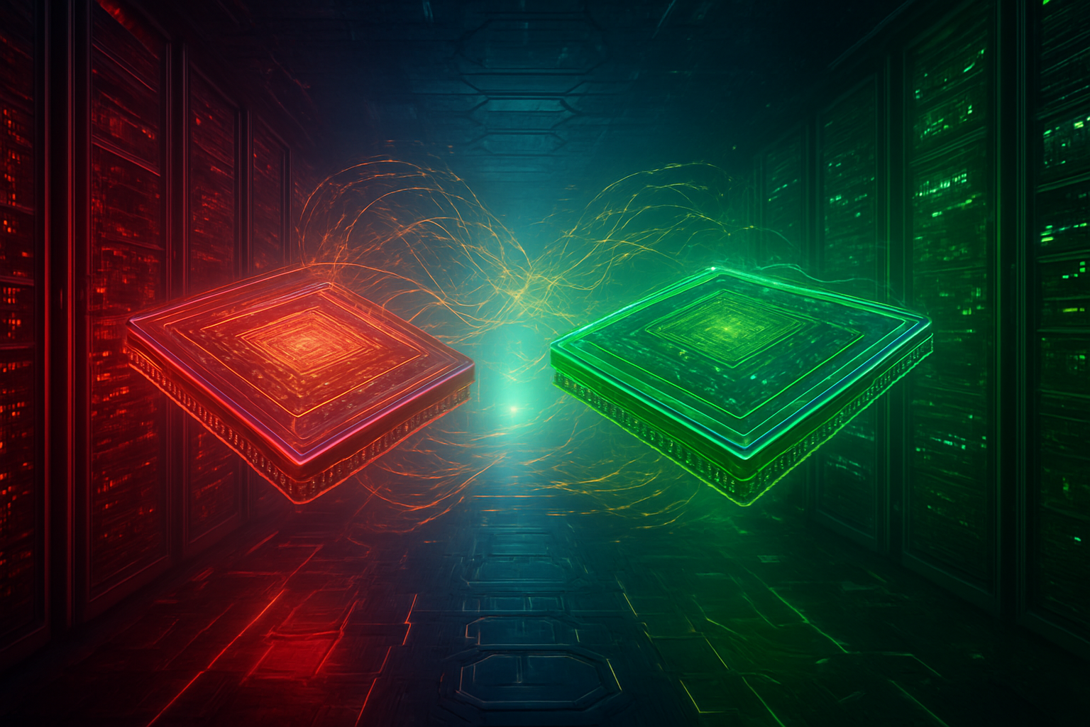
As the artificial intelligence industry moves into its "Industrialization Phase" in late 2025, the focus has shifted from high-level model architectures to the fundamental physical constraints of computing. The announcement of a comprehensive new resource from Stanford Advanced Materials (SAM), titled "Silicon Wafer Technology and Supplier Selection," marks a pivotal moment for hardware engineers and procurement teams. This guide arrives at a critical juncture where the success of next-generation AI accelerators, such as the upcoming Rubin architecture from NVIDIA (NASDAQ: NVDA), depends entirely on the microscopic perfection of the silicon substrates beneath them.
The immediate significance of this development lies in the industry's transition to 2nm and 1.4nm process nodes. At these infinitesimal scales, the silicon wafer is no longer a passive carrier but a complex, engineered component that dictates power efficiency, thermal management, and—most importantly—manufacturing yield. As AI labs demand millions of high-performance chips, the ability to source ultra-pure, perfectly flat wafers has become the ultimate competitive moat, separating the leaders of the silicon age from those struggling with supply chain bottlenecks.
The Technical Frontier: 11N Purity and Backside Power Delivery
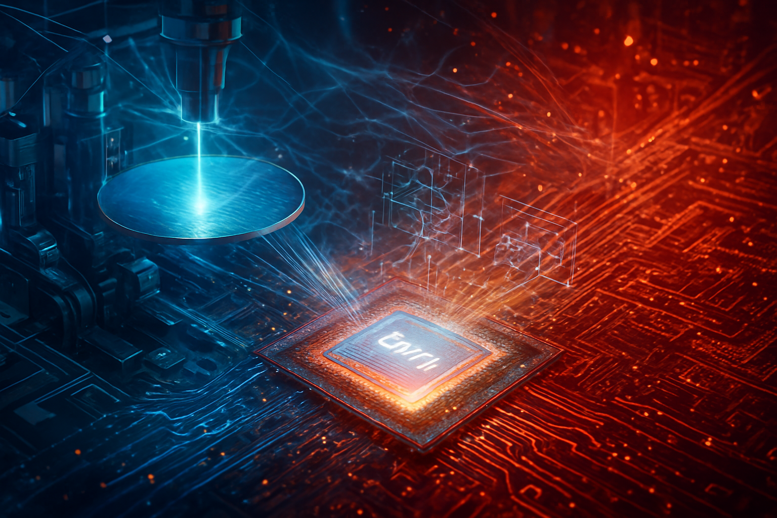
The technical specifications for silicon wafers in late 2025 have reached levels of precision previously thought impossible. According to the new SAM resources, the industry benchmark for advanced logic nodes has officially moved to 11N purity (99.999999999%). This level of decontamination is essential for the Gate-All-Around (GAA) transistor architectures used by Taiwan Semiconductor Manufacturing Company (NYSE: TSM) and Samsung Electronics (KRX: 005930). At this scale, even a single foreign atom can cause a catastrophic failure in the ultra-fine circuitry of an AI processor.
Beyond purity, the SAM guide highlights the rise of specialized substrates like Epitaxial (Epi) wafers and Fully Depleted Silicon-on-Insulator (FD-SOI). Epi wafers are now critical for the implementation of Backside Power Delivery (BSPDN), a breakthrough technology that moves power routing to the rear of the wafer to reduce "routing congestion" on the front. This allows for more dense transistor placement, directly enabling the massive parameter counts of 2026-class Large Language Models (LLMs). Furthermore, the guide details the requirement for "ultra-flatness," where the Total Thickness Variation (TTV) must be less than 0.3 microns to accommodate the extremely shallow depth of focus in High-NA EUV lithography machines.
Strategic Shifts: From Transactions to Foundational Partnerships
This advancement in wafer technology is forcing a radical shift in how tech giants and startups approach their supply chains. Major players like Intel (NASDAQ: INTC) and NVIDIA are moving away from transactional purchasing toward what SAM calls "Foundational Technology Partnerships." In this model, chip designers and wafer suppliers collaborate years in advance to tailor substrate characteristics—such as resistivity and crystal orientation—to the specific needs of a chip's architecture.
The competitive implications are profound. Companies that secure "priority capacity" for 300mm wafers with advanced Epi layers will have a significant advantage in bringing their chips to market. We are also seeing a "Shift Left" strategy, where procurement teams are prioritizing regional hubs to mitigate geopolitical risks. For instance, the expansion of GlobalWafers (TWO: 6488) in the United States, supported by the CHIPS Act, has become a strategic anchor for domestic fabrication sites in Arizona and Texas. Startups that fail to adopt these sophisticated supplier selection strategies risk being "priced out" or "waited out" as the 9.2 million wafer-per-month global capacity is increasingly pre-allocated to the industry's titans.
Geopolitics and the Sustainability of the AI Boom
The wider significance of these wafer advancements extends into the realms of geopolitics and environmental sustainability. The silicon wafer is the first link in the AI value chain, and its production is concentrated in a handful of high-tech facilities. The SAM guide emphasizes that "Geopolitical Resilience" is now a top-tier metric in supplier selection, reflecting the ongoing tensions over semiconductor sovereignty. As nations race to build "sovereign AI" clouds, the demand for locally sourced, high-grade silicon has turned a commodity market into a strategic battlefield.
Furthermore, the environmental impact of wafer production is under intense scrutiny. The Czochralski (CZ) process used to grow silicon crystals is energy-intensive and requires vast amounts of ultrapure water. In response, the latest industry standards highlighted by SAM prioritize suppliers that utilize AI-driven manufacturing to reduce chemical waste and implement closed-loop water recycling. This shift ensures that the AI revolution does not come at an unsustainable environmental cost, aligning the hardware industry with global ESG (Environmental, Social, and Governance) mandates that have become mandatory for public investment in 2025.
The Horizon: 450mm Wafers and 2D Materials
Looking ahead, the industry is already preparing for the next set of challenges. While 300mm wafers remain the standard, research into Panel-Level Packaging—utilizing 600mm x 600mm square substrates—is gaining momentum as a way to increase the yield of massive AI die sizes. Experts predict that the next three years will see the integration of 2D materials like molybdenum disulfide (MoS2) directly onto silicon wafers, potentially allowing for "3D stacked" logic that could bypass the physical limits of current transistor scaling.
However, these future applications face significant hurdles. The transition to larger formats or exotic materials requires a multi-billion dollar overhaul of the entire lithography and etching ecosystem. The consensus among industry analysts is that the near-term focus will remain on refining the "Advanced Packaging" interface, where the quality of the silicon interposer—the bridge between the chip and its memory—is just as critical as the processor wafer itself.
Conclusion: The Bedrock of the Intelligence Age
The release of the Stanford Advanced Materials resources serves as a stark reminder that the "magic" of artificial intelligence is built on a foundation of material science. As we have seen, the difference between a world-leading AI model and a failed product often comes down to the sub-micron flatness and 11N purity of a silicon disk. The advancements in wafer technology and the evolution of supplier selection strategies are not merely technical footnotes; they are the primary drivers of the AI economy.
In the coming months, keep a close watch on the quarterly earnings of major wafer suppliers and the progress of "backside power" integration in consumer and data center chips. As the industry prepares for the 1.4nm era, the companies that master the complexities of the silicon substrate will be the ones that define the next decade of human innovation.
This content is intended for informational purposes only and represents analysis of current AI developments.
TokenRing AI delivers enterprise-grade solutions for multi-agent AI workflow orchestration, AI-powered development tools, and seamless remote collaboration platforms.
For more information, visit https://www.tokenring.ai/.