The landscape of artificial intelligence underwent a tectonic shift this past month at CES 2026, as NVIDIA (NASDAQ: NVDA) officially unveiled its "Vera Rubin" architecture. Named after the visionary astronomer who provided the first evidence of dark matter, the Rubin platform is designed to illuminate the next era of "agentic AI"—autonomous systems capable of complex reasoning and multi-step execution. This launch marks the culmination of NVIDIA’s aggressive transition to a yearly R&D cycle, effectively doubling the pace of innovation that the industry had previously grown accustomed to.
The Rubin architecture is not merely an incremental update; it represents a full-stack reimagining of the data center. By succeeding the highly successful Blackwell architecture, Rubin pushes the boundaries of what is possible in silicon and systems engineering. With the introduction of the new Vera CPU and the HBM4-powered Rubin GPU, NVIDIA is positioning itself not just as a chipmaker, but as the architect of the unified AI factory. The immediate significance is clear: as enterprises race to deploy trillion-parameter models, NVIDIA has provided the first hardware platform capable of running these workloads with five times the efficiency of its predecessor.
The Architecture of the Infinite: Technical Mastery in the Rubin Era
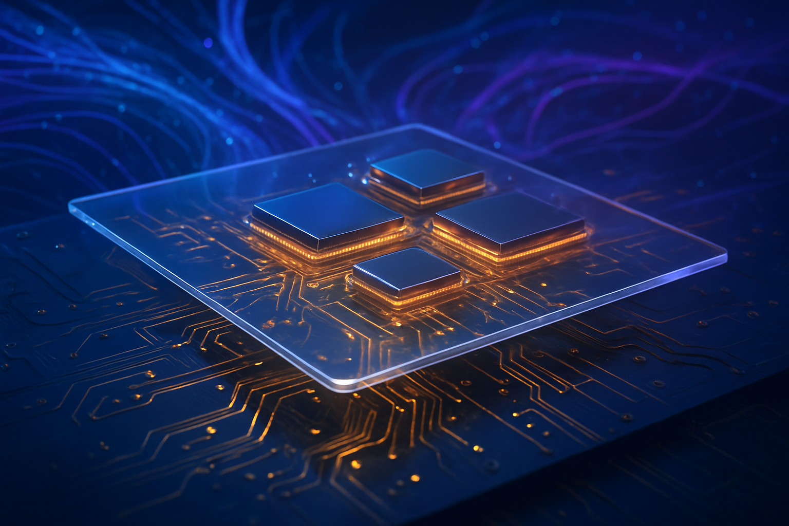
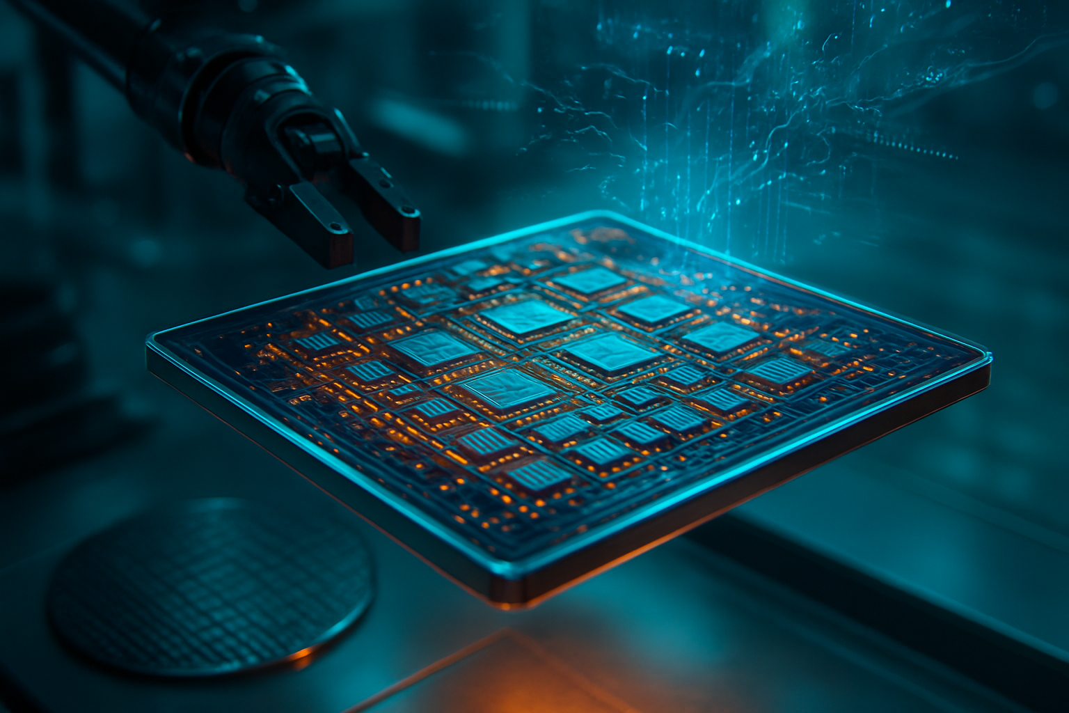
The technical specifications of the Vera Rubin platform are nothing short of staggering. At the heart of the system is the Rubin GPU, the first in the industry to fully embrace High Bandwidth Memory 4 (HBM4). Each GPU boasts 288GB of HBM4 memory, delivering a massive 22 TB/s of aggregate bandwidth. This leap is specifically engineered to overcome the "memory wall," a long-standing bottleneck where data movement speeds lagged behind processing power. By nearly tripling the bandwidth of the Blackwell generation, NVIDIA has enabled a 5x increase in inference performance, reaching up to 50 petaflops of NVFP4 compute.
Perhaps the most significant architectural shift is the introduction of the Vera CPU, also referred to as the "Versa" platform. Built on 88 custom "Olympus" cores utilizing the Arm v9.2 architecture, the Vera CPU represents NVIDIA’s most ambitious foray into general-purpose compute. Unlike previous generations where CPUs were often a secondary consideration to the GPU, the Vera CPU is designed to handle the complex serial processing and orchestration required for modern AI agents. In a major strategic pivot, NVIDIA has announced that the Vera CPU will be available as a standalone product, a move that provides 1.2 TB/s of memory bandwidth and directly challenges traditional data center processors.
The flagship implementation of this hardware is the NVL72 rack-scale system. Functioning as a single, liquid-cooled supercomputer, the NVL72 integrates 36 Vera CPUs and 72 Rubin GPUs into a unified fabric. Utilizing the new NVLink 6 Switch, the rack provides 260 TB/s of total bandwidth—a figure that NVIDIA CEO Jensen Huang noted is "greater than the traffic of the entire public internet." This high-density configuration allows for 3.6 exaFLOPS of inference performance in a single rack, making it the most power-dense AI infrastructure ever produced for the commercial market.
Market Dominance and the Standalone CPU Play
The announcement has sent shockwaves through the semiconductor industry, particularly impacting Intel (NASDAQ: INTC) and AMD (NASDAQ: AMD). By offering the Vera CPU as a standalone product, NVIDIA is moving into Intel’s historical stronghold: the general-purpose server market. Market analysts noted that Intel’s stock fell over 4% following the announcement, as the Vera CPU’s specialized AI capabilities and superior memory bandwidth make it an attractive alternative for data centers that are increasingly pivoting toward AI-first architectures.
AMD, meanwhile, attempted to counter NVIDIA’s momentum at CES with its Instinct MI455X and the Helios rack platform. While AMD’s offering boasts a higher raw memory capacity of 432GB, it lags behind Rubin in bandwidth and integrated ecosystem support. The competitive landscape is now defined by NVIDIA’s "speed-of-light" execution; by moving to a yearly release cadence (Blackwell in 2024, Rubin in 2026, and the teased "Feynman" architecture for 2027), NVIDIA is forcing its rivals into a perpetual state of catch-up. This rapid-fire cycle creates a significant strategic advantage, as major cloud service providers (CSPs) like Amazon (NASDAQ: AMZN) and Microsoft (NASDAQ: MSFT) are likely to prioritize the hardware that offers the fastest path to lowering the "cost per token" in AI inference.
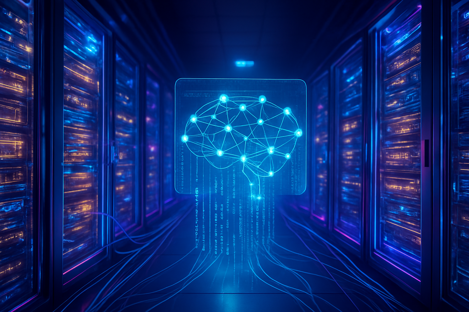
The Broader Implications: Agentic AI and the Power Paradox
The Rubin architecture arrives at a critical juncture in the AI landscape. We are moving away from simple chatbots and toward "Agentic AI"—systems that can manage their own workflows, use tools, and solve multi-part problems autonomously. These agents require massive amounts of "thinking time" (inference), and the Rubin platform’s 5x inference boost is tailor-made for this shift. By focusing on inference efficiency—offering up to 8x more compute per watt—NVIDIA is addressing one of the most pressing concerns in the industry: the soaring energy demands of global data centers.
However, this advancement also brings potential concerns to the forefront. The sheer density of the NVL72 racks requires sophisticated liquid cooling and a power grid capable of supporting exascale workloads. Critics point out that while efficiency per watt is increasing, the total power draw of these massive AI clusters continues to climb. Comparisons are already being drawn to previous AI milestones, such as the introduction of the Transformer model or the launch of the original H100; however, Rubin feels different. It marks the transition of AI from a specialized research tool into the foundational infrastructure of the modern global economy.
Looking Toward the Feynman Horizon
As the industry digests the implications of the Rubin launch, eyes are already turning toward the future. NVIDIA’s roadmap suggests that the Rubin era will be followed by the "Feynman" architecture in 2027 or 2028. Near-term developments will likely focus on the widespread deployment of the NVL72 racks across global "AI Factories." We can expect to see new classes of autonomous software agents that were previously too computationally expensive to run, ranging from real-time scientific simulation to fully autonomous corporate operations.
The challenges ahead are largely logistical and environmental. Addressing the heat dissipation of such high-density racks and ensuring a stable supply chain for HBM4 memory will be the primary hurdles for NVIDIA in the coming year. Furthermore, the industry will be watching closely to see how the software ecosystem evolves to take advantage of the Vera CPU’s custom Olympus cores. Predictions from industry experts suggest that by the time Rubin reaches full market penetration in late 2026, the concept of a "data center" will have been entirely redefined as a "liquid-cooled AI inference engine."
A New Benchmark for the Silicon Age
NVIDIA’s Vera Rubin architecture is more than just a faster chip; it is a declaration of intent. By integrating custom CPUs, next-generation HBM4 memory, and massive rack-scale networking into a yearly release cycle, NVIDIA has set a pace that defines the "Golden Age of AI." The key takeaways from CES 2026 are clear: inference is the new currency, and the ability to scale to 72 GPUs in a single rack is the new standard for enterprise readiness.
As we look toward the coming months, the significance of the Rubin platform in AI history will likely be measured by the autonomy of the agents it powers. This development solidifies NVIDIA's position at the center of the technological universe, challenging competitors to reinvent themselves or risk obsolescence. For now, the "Vera Rubin" era has begun, and the search for the next breakthrough in the dark matter of artificial intelligence continues at an unprecedented speed.
This content is intended for informational purposes only and represents analysis of current AI developments.
TokenRing AI delivers enterprise-grade solutions for multi-agent AI workflow orchestration, AI-powered development tools, and seamless remote collaboration platforms.
For more information, visit https://www.tokenring.ai/.