In a landmark moment for the American technology sector, Texas Instruments (NASDAQ: TXN) officially commenced production at its newest semiconductor fabrication plant in Sherman, Texas, on December 17, 2025. The grand opening of the "SM1" facility marks the first phase of a massive four-factory "mega-site" that represents one of the largest private-sector investments in Texas history. This development is a cornerstone of the United States' broader strategy to reclaim its lead in global semiconductor manufacturing, providing the foundational hardware necessary to power everything from electric vehicles to the burgeoning infrastructure of the artificial intelligence era.
The ribbon-cutting ceremony, attended by Texas Governor Greg Abbott and TI President and CEO Haviv Ilan, signals a shift in the global supply chain. As the first of four planned facilities on the 1,200-acre site begins its operations, it brings immediate relief to industries that have long struggled with the volatility of overseas chip production. By focusing on high-volume, 300-millimeter wafer manufacturing, Texas Instruments is positioning itself as the primary domestic supplier of the analog and embedded processing chips that serve as the "nervous system" for modern electronics.
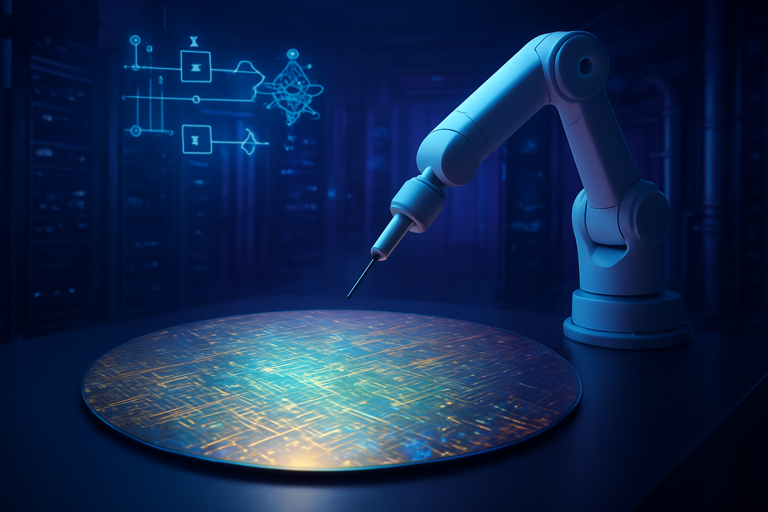
Foundational Tech: The Power of 300mm Wafers
The SM1 facility is a marvel of modern industrial engineering, specifically designed to produce 300-millimeter (12-inch) wafers. This technical choice is significant; 300mm wafers provide roughly 2.3 times more surface area than the older 200mm standard, allowing TI to produce millions more chips per wafer while drastically lowering the cost per unit. The plant focuses on "foundational" process nodes ranging from 65nm to 130nm. While these are not the "leading-edge" nodes used for high-end CPUs, they are the industry standard for analog chips that manage power, sense environmental data, and convert real-world signals into digital data—components that are indispensable for AI hardware and industrial robotics.
Industry experts have noted that the Sherman facility's reliance on these mature nodes is a strategic masterstroke. While much of the industry's attention is focused on sub-5nm logic chips, the global shortage of 2021-2022 proved that a lack of simple analog components can halt entire production lines for automobiles and medical devices. By securing high-volume domestic production of these parts, TI is filling a critical gap in the U.S. electronics ecosystem. The SM1 plant is expected to produce tens of millions of chips daily at full capacity, utilizing highly automated cleanrooms that minimize human error and maximize yield.
Initial reactions from the semiconductor research community have been overwhelmingly positive. Analysts at Gartner and IDC have highlighted that TI’s "own-and-operate" strategy—where the company controls every step from wafer fabrication to assembly and test—gives them a distinct advantage over "fabless" competitors who rely on external foundries like TSMC (NYSE: TSM). This vertical integration, now bolstered by the Sherman site, ensures a level of supply chain predictability that has been absent from the market for years.
Industry Impact and Competitive Moats
The opening of the Sherman site creates a significant competitive moat for Texas Instruments, particularly against international rivals in Europe and Asia. By manufacturing at scale on 300mm wafers domestically, TI can offer more competitive pricing and shorter lead times to major U.S. customers in the automotive and industrial sectors. Companies like Ford (NYSE: F) and General Motors (NYSE: GM), which are pivoting heavily toward electric and autonomous vehicles, stand to benefit from a reliable, local source of power management and sensor chips.
For the broader tech landscape, this move puts pressure on other domestic players like Intel (NASDAQ: INTC) and Micron (NASDAQ: MU) to accelerate their own CHIPS Act-funded projects. While Intel focuses on high-performance logic and Micron on memory, TI’s dominance in the analog space ensures that the "supporting cast" of chips required for any AI server or smart device remains readily available. This helps stabilize the entire domestic hardware market, reducing the "bullwhip effect" of supply chain disruptions that often lead to price spikes for consumers and enterprise tech buyers.
Furthermore, the Sherman mega-site is likely to disrupt the existing reliance on older, 200mm-based foundries in Asia. As TI transitions its production to the more efficient 300mm Sherman facility, it can effectively underprice competitors who are stuck using older, less efficient equipment. This strategic advantage is expected to increase TI's market share in the industrial automation and communications sectors, where reliability and cost-efficiency are the primary drivers of procurement.
The CHIPS Act and the AI Infrastructure
The significance of the Sherman opening extends far beyond Texas Instruments' balance sheet; it is a major victory for the CHIPS and Science Act of 2022. TI has secured a preliminary agreement for $1.61 billion in direct federal funding, with a significant portion earmarked specifically for the Sherman site. When combined with an estimated $6 billion to $8 billion in investment tax credits, the project serves as a premier example of how public-private partnerships can revitalize domestic manufacturing. This aligns with the U.S. government’s goal of reducing dependence on foreign entities for critical technology components.
In the context of the AI revolution, the Sherman site provides the "hidden" infrastructure that makes AI possible. While GPUs get the headlines, those GPUs cannot function without the sophisticated power management systems and signal chain components that TI specializes in. Governor Greg Abbott emphasized this during the ceremony, noting that Texas is becoming the "home for cutting-edge semiconductor manufacturing" that will define the future of AI and space exploration. The facility also addresses long-standing concerns regarding national security, ensuring that the chips used in defense systems and critical infrastructure are "Made in America."
The local impact on Sherman and the surrounding North Texas region is equally profound. The project has already supported over 20,000 construction jobs and is expected to create 3,000 direct, high-wage positions at TI once all four fabs are operational. To sustain this workforce, TI has partnered with over 40 community colleges and high schools to create a pipeline of technicians. This focus on "middle-skill" jobs provides a blueprint for how the tech industry can drive economic mobility without requiring every worker to have an advanced engineering degree.
Future Horizons: SM2 and Beyond
Looking ahead, the SM1 facility is only the beginning. Construction is already well underway for SM2, with SM3 and SM4 planned to follow sequentially through the end of the decade. The total investment at the Sherman site could eventually reach $40 billion, creating a semiconductor cluster that rivals any in the world. As these additional fabs come online, Texas Instruments will have the capacity to meet the projected surge in demand for chips used in 6G communications, advanced robotics, and the next generation of renewable energy systems.
One of the primary challenges moving forward will be the continued scaling of the workforce. As more facilities open across the U.S.—including Intel’s site in Ohio and Micron’s site in New York—competition for specialized talent will intensify. Experts predict that the next few years will see a massive push for automation within the fabs themselves to offset potential labor shortages. Additionally, as the industry moves toward more integrated "System-on-Chip" (SoC) designs, TI will likely explore new ways to package its analog components closer to the logic chips they support.
A New Era for American Silicon
The grand opening of Texas Instruments' SM1 facility in Sherman is more than just a corporate milestone; it is a signal that the "Silicon Prairie" has arrived. By successfully leveraging CHIPS Act incentives to build a massive, 300mm-focused manufacturing hub, TI has demonstrated a viable path for the return of American industrial might. The key takeaways are clear: domestic supply chain security is now a top priority, and the foundational chips that power our world are finally being produced at scale on U.S. soil.
As we move into 2026, the tech industry will be watching closely to see how quickly SM1 ramps up to full production and how the availability of these chips affects the broader market. This development marks a turning point in semiconductor history, proving that with the right combination of private investment and government support, the U.S. can maintain its technological sovereignty. For now, the lights are on in Sherman, and the first wafers are already moving through the line, marking the start of a new era in American innovation.
This content is intended for informational purposes only and represents analysis of current AI developments.
TokenRing AI delivers enterprise-grade solutions for multi-agent AI workflow orchestration, AI-powered development tools, and seamless remote collaboration platforms.
For more information, visit https://www.tokenring.ai/.