As the artificial intelligence revolution accelerates into late 2025, the industry’s focus has shifted from the raw transistor counts of chips to the sophisticated architecture that holds them together. While massive Large Language Models (LLMs) continue to demand unprecedented compute power, the primary bottleneck is no longer just the speed of the processor, but the "memory wall"—the physical limit of how fast data can travel between memory and logic. Advanced packaging has emerged as the critical solution to this crisis, transforming from a secondary manufacturing step into the primary frontier of semiconductor innovation.
At the heart of this transition is Kulicke and Soffa Industries (NASDAQ: KLIC), a company that has successfully pivoted from its legacy as a leader in traditional wire bonding to becoming a pivotal player in the high-stakes world of AI advanced packaging. By enabling the complex stacking and interconnectivity required for High Bandwidth Memory (HBM) and chiplet architectures, KLIC is proving that the future of AI performance will be won not just by the designers of chips, but by the masters of assembly.
The Technical Leap: Solving the Memory Wall with Fluxless TCB
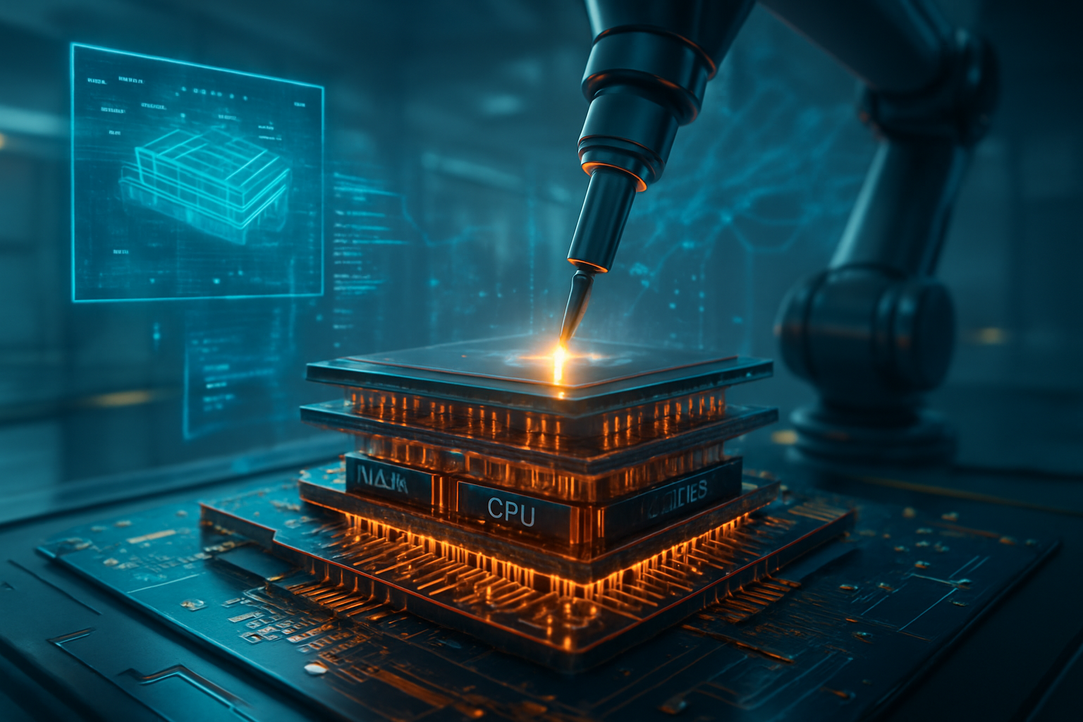
The technical challenge of 2025 AI hardware lies in the transition from 2D layouts to 2.5D and 3D heterogeneous architectures. Traditional wire bonding, which uses thin gold or copper wires to connect chips to their packages, is increasingly insufficient for the ultra-high-speed requirements of AI GPUs like the Blackwell series from NVIDIA (NASDAQ: NVDA). These modern accelerators require thousands of microscopic connections, known as micro-bumps, to be placed with sub-10-micron precision. This is where KLIC’s Advanced Solutions segment, specifically its APTURA™ series, has become indispensable.
KLIC’s breakthrough technology is Fluxless Thermo-Compression Bonding (FTC). Unlike traditional methods that use chemical flux to remove oxidation—a process that leaves behind residues difficult to clean at the fine pitches required for HBM4—KLIC’s FTC uses a formic acid vapor in-situ. This "dry" process ensures a cleaner, more reliable bond, allowing for an interconnect pitch as small as 8 micrometers. This level of precision is vital for the 12- and 16-layer HBM stacks that provide the 4TB/s+ bandwidth necessary for next-generation AI training.
Furthermore, KLIC has introduced the CuFirst™ Hybrid Bonding technology. While traditional bonding relies on heat and pressure to melt solder bumps, hybrid bonding allows copper-to-copper interconnects at room temperature, followed by a dielectric seal. This "bumpless" approach significantly reduces the distance data must travel, cutting latency and reducing power consumption by up to 40% compared to previous generations. By providing these tools, KLIC is enabling the industry to move beyond the physical limits of traditional silicon scaling, a trend often referred to as "More than Moore."
Market Impact: Navigating the CoWoS Supply Chain
The strategic importance of advanced packaging is best reflected in the supply chain of Taiwan Semiconductor Manufacturing Company (NYSE: TSM), the world’s leading foundry. In late 2025, TSMC’s Chip-on-Wafer-on-Substrate (CoWoS) capacity has become the most valuable real estate in the tech world. As TSMC doubled its CoWoS capacity to roughly 80,000 wafers per month to meet the demands of NVIDIA and Advanced Micro Devices (NASDAQ: AMD), the equipment providers that qualify for these lines have seen their market positions solidify.
KLIC has successfully broken into this elite circle, qualifying its fluxless TCB systems for TSMC’s CoWoS-L process. This has placed KLIC in direct competition with incumbents like ASMPT (HKG: 0522) and BE Semiconductor Industries (AMS: BESI). While ASMPT remains a high-volume leader in the broader market, KLIC’s specialized focus on fluxless technology has made it a preferred partner for the high-yield, high-reliability requirements of AI server modules. For companies like NVIDIA, having multiple qualified equipment vendors like KLIC ensures a more resilient supply chain and helps mitigate the chronic shortages that plagued the industry in 2023 and 2024.
The shift also benefits AMD, which has been more aggressive in adopting 3D chiplet architectures. AMD’s MI350 series, launched earlier this year, utilizes 3D hybrid bonding to stack compute chiplets directly onto I/O dies. This architectural choice gives AMD a competitive edge in power efficiency, a metric that has become as important as raw speed for data center operators. As these tech giants battle for AI supremacy, their reliance on advanced packaging equipment providers has effectively turned companies like KLIC into the "arms dealers" of the AI era.
The Wider Significance: Beyond Moore's Law
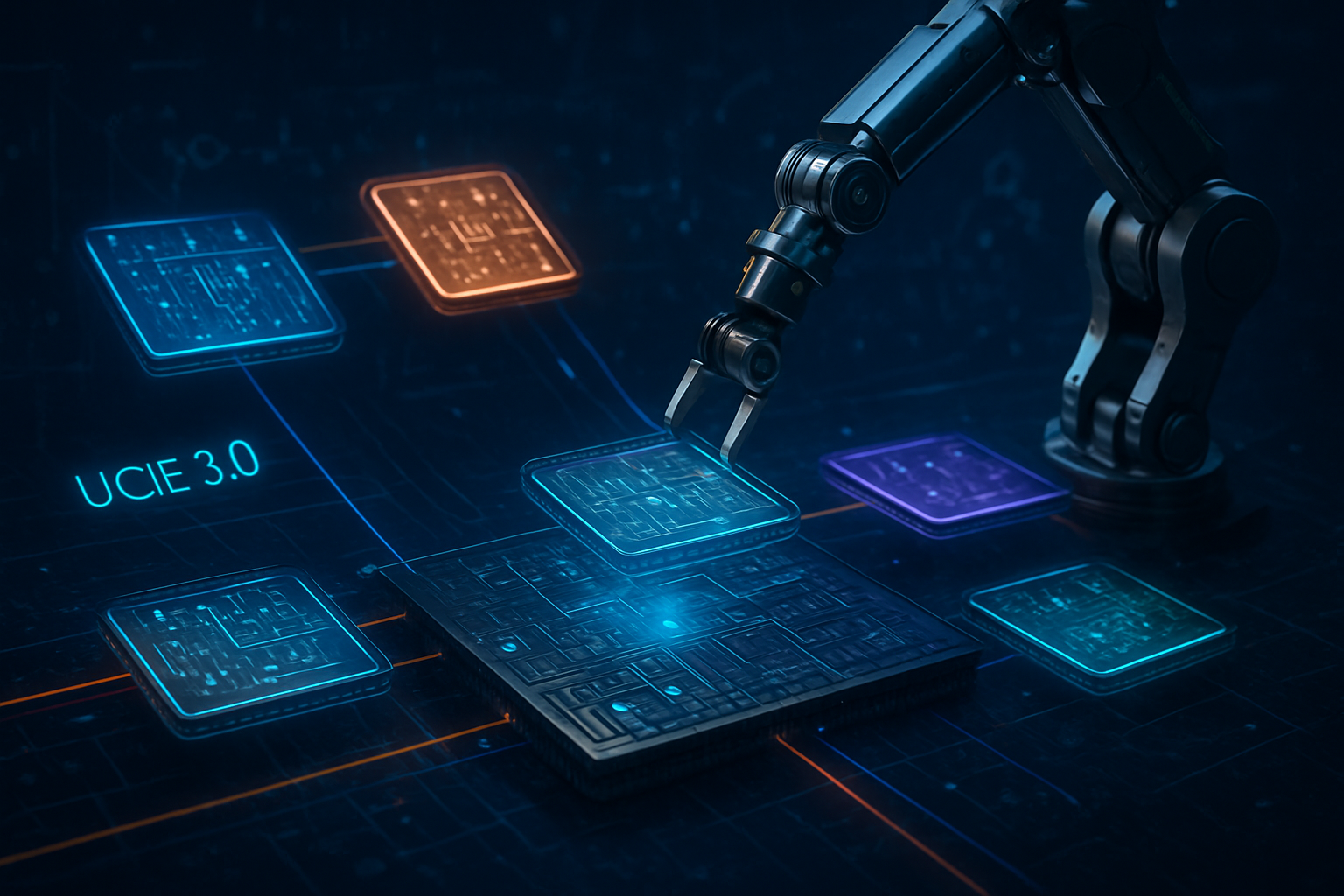
The rise of advanced packaging marks a fundamental shift in the semiconductor landscape. For decades, the industry followed Moore’s Law, doubling transistor density every two years by shrinking the size of individual transistors. However, as transistors approach the atomic scale, the cost and complexity of further shrinking have skyrocketed. Advanced packaging offers a way out of this economic trap by allowing engineers to "disaggregate" the chip into smaller, specialized chiplets that can be manufactured on different process nodes and then stitched together.
This trend has profound geopolitical implications. Under the U.S. CHIPS Act and similar initiatives in Europe and Japan, there is a renewed focus on bringing packaging capabilities back to Western shores. Historically, packaging was seen as a low-margin, labor-intensive "back-end" process that was outsourced to Southeast Asia. In 2025, it is recognized as a high-tech, high-margin "mid-end" process essential for national security and technological sovereignty. KLIC, as a U.S.-headquartered company with a deep global footprint, is uniquely positioned to benefit from this reshoring trend.
Furthermore, the environmental impact of AI is under intense scrutiny. The energy required to move data between a processor and its memory can often exceed the energy used for the actual computation. By using KLIC’s advanced bonding technologies to place memory closer to the logic, the industry is making significant strides in "Green AI." Reducing the parasitic capacitance of interconnects is no longer just a technical goal; it is a sustainability mandate for the world's largest data center operators.
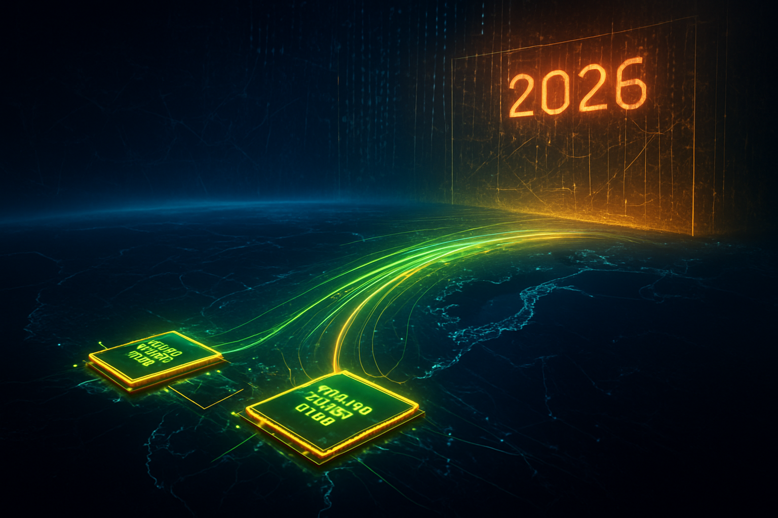
Future Outlook: The Road to Glass Substrates and CPO
Looking toward 2026 and 2027, the roadmap for advanced packaging includes even more radical shifts. One of the most anticipated developments is the move from organic substrates to glass substrates. Glass offers superior flatness and thermal stability, which will be necessary as AI chips grow larger and hotter. Companies like KLIC are already in R&D phases for equipment that can handle the unique handling and bonding requirements of glass, which is far more brittle than the materials used today.
Another major horizon is Co-Packaged Optics (CPO). As electrical signals struggle to maintain integrity over longer distances, the industry is looking to integrate optical fibers directly into the chip package. This would allow data to be transmitted via light rather than electricity, virtually eliminating the "memory wall" and enabling massive clusters of GPUs to act as a single, giant processor. The precision required to align these optical fibers is an order of magnitude higher than even today’s most advanced TCB, representing the next great challenge for KLIC’s engineering teams.
Experts predict that by 2027, the "Year of HBM4," hybrid bonding will move from niche applications into high-volume manufacturing. While TCB remains the workhorse for today's Blackwell and MI350 chips, the transition to hybrid bonding will require a massive new cycle of capital expenditure. The winners will be those who can provide high-throughput machines that maintain sub-micron accuracy in a high-volume factory environment.
A New Era of Semiconductor Assembly
The transformation of Kulicke and Soffa from a wire-bonding specialist into an advanced packaging powerhouse is a microcosm of the broader shift in the semiconductor industry. As AI models grow in complexity, the "package" has become as vital as the "chip." The ability to stack, connect, and cool these massive silicon systems is now the primary determinant of who leads the AI race.
Key takeaways from this development include the critical role of fluxless bonding in improving yields for HBM4 and the strategic importance of being qualified in the TSMC CoWoS supply chain. As we move further into 2026, the industry will be watching for the first high-volume applications of glass substrates and the continued adoption of hybrid bonding.
For investors and industry observers, the message is clear: the next decade of AI breakthroughs will not just be written in code or silicon, but in the microscopic copper interconnects that bind them together. Advanced packaging is no longer the final step in the process; it is the foundation upon which the future of artificial intelligence is being built.
This content is intended for informational purposes only and represents analysis of current AI developments.
TokenRing AI delivers enterprise-grade solutions for multi-agent AI workflow orchestration, AI-powered development tools, and seamless remote collaboration platforms.
For more information, visit https://www.tokenring.ai/.