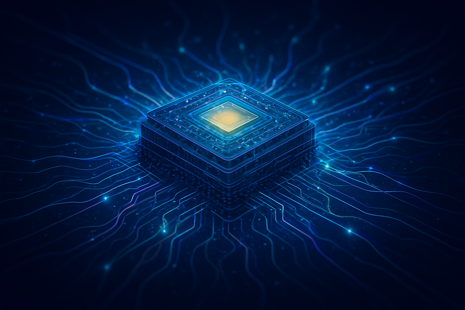
As of December 2025, the semiconductor industry has reached a historic inflection point. For decades, the primary metric of progress was the "node"—the relentless shrinking of transistors to pack more power into a single slice of silicon. However, as physical limits and skyrocketing costs have slowed traditional Moore’s Law scaling, the focus has shifted from how a chip is made to how it is assembled. Advanced 3D-IC packaging, led by technologies such as CoWoS and SoIC, has emerged as the true engine of the AI revolution, determining which companies can build the massive "super-chips" required to power the next generation of frontier AI models.
The immediate significance of this shift cannot be overstated. In late 2025, the bottleneck for AI progress is no longer just the availability of advanced lithography machines, but the capacity of specialized packaging facilities. With AI giants like Nvidia (NASDAQ: NVDA) and AMD (NASDAQ: AMD) pushing the boundaries of chip size, the ability to "stitch" multiple dies together with near-monolithic performance has become the defining competitive advantage. This move toward "System-on-Package" (SoP) architectures represents the most significant change in computer engineering since the invention of the integrated circuit itself.
The Architecture of Scale: CoWoS-L and SoIC-X
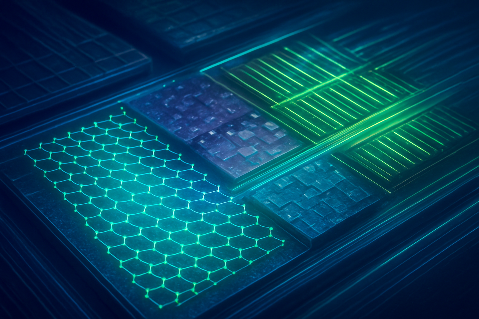
The technical foundation of this new era rests on two pillars from Taiwan Semiconductor Manufacturing Co. (NYSE: TSM): CoWoS (Chip on Wafer on Substrate) and SoIC (System on Integrated Chips). In late 2025, the industry has transitioned to CoWoS-L, a 2.5D packaging technology that uses an organic interposer with embedded Local Silicon Interconnect (LSI) bridges. Unlike previous iterations that relied on a single, massive silicon interposer, CoWoS-L allows for packages that exceed the "reticle limit"—the maximum size a lithography machine can print. This enables Nvidia’s Blackwell and the upcoming Rubin architectures to link multiple GPU dies with a staggering 10 TB/s of chip-to-chip bandwidth, effectively making two separate pieces of silicon behave as one.
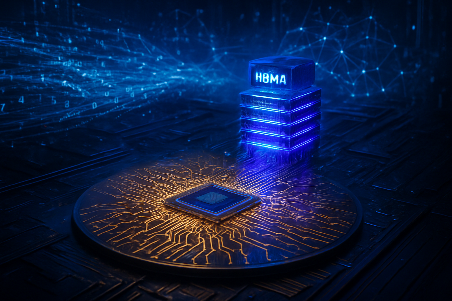
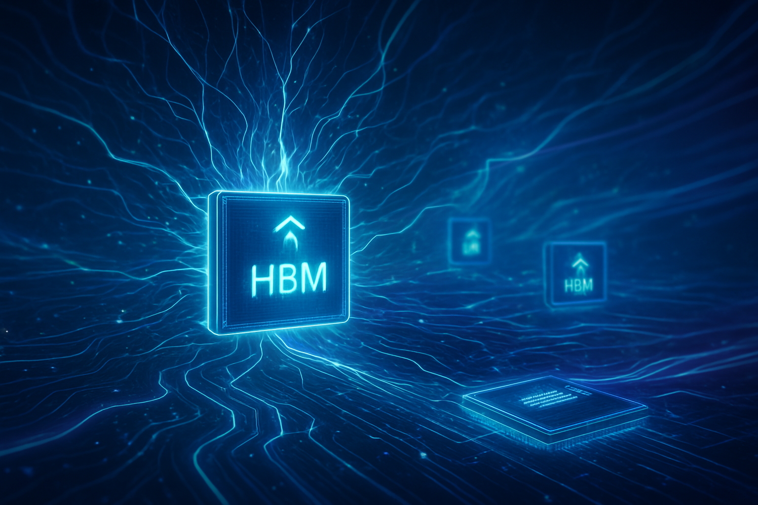
Complementing this is SoIC-X, a true 3D stacking technology that uses "hybrid bonding" to fuse dies vertically. By late 2025, TSMC has achieved a 6μm bond pitch, allowing for over one million interconnects per square millimeter. This "bumpless" bonding eliminates the traditional micro-bumps used in older packaging, drastically reducing electrical impedance and power consumption. While AMD was an early pioneer of this with its MI300 series, 2025 has seen Nvidia adopt SoIC for its high-end Rubin chips to integrate logic and I/O tiles more efficiently. This differs from previous approaches by moving the "interconnect" from the circuit board into the silicon itself, solving the "Memory Wall" by placing High Bandwidth Memory (HBM) microns away from the compute cores.
Initial reactions from the research community have been transformative. Experts note that these packaging technologies have allowed for a 3.5x increase in effective chip area compared to monolithic designs. However, the complexity of these 3D structures has introduced new challenges in thermal management. With AI accelerators now drawing upwards of 1,200W, the industry has been forced to innovate in liquid cooling and backside power delivery to prevent these multi-layered "silicon skyscrapers" from overheating.
A New Power Dynamic: Foundries, OSATs, and the "Nvidia Tax"
The rise of advanced packaging has fundamentally altered the business landscape of Silicon Valley. TSMC remains the dominant force, with its packaging capacity projected to reach 80,000 wafers per month by the end of 2025. This dominance has allowed TSMC to capture a larger share of the total value chain, as packaging now accounts for a significant portion of a chip's final cost. However, the persistent "CoWoS shortage" of 2024 and 2025 has created an opening for competitors. Intel (NASDAQ: INTC) has positioned its Foveros and EMIB technologies as a strategic "escape valve," attracting major customers like Apple (NASDAQ: AAPL) and even Nvidia, which has reportedly diversified some of its packaging needs to Intel’s facilities to mitigate supply risks.
This shift has also elevated the status of Outsourced Semiconductor Assembly and Test (OSAT) providers. Companies like Amkor Technology (NASDAQ: AMKR) and ASE Technology Holding (NYSE: ASX) are no longer just "back-end" service providers; they are now critical partners in the AI supply chain. By late 2025, OSATs have taken over the production of more mature advanced packaging variants, allowing foundries to focus their high-end capacity on the most complex 3D-IC projects. This "Foundry 2.0" model has created a tripartite ecosystem where the ability to secure packaging slots is as vital as securing the silicon itself.
Perhaps the most disruptive trend is the move by AI labs like OpenAI and Meta (NASDAQ: META) to design their own custom ASICs. By bypassing the "Nvidia Tax" and working directly with Broadcom (NASDAQ: AVGO) and TSMC, these companies are attempting to secure their own dedicated packaging allocations. Meta, for instance, has secured an estimated 50,000 CoWoS wafers for its MTIA v3 chips in 2026, signaling a future where the world’s largest AI consumers are also its most influential hardware architects.
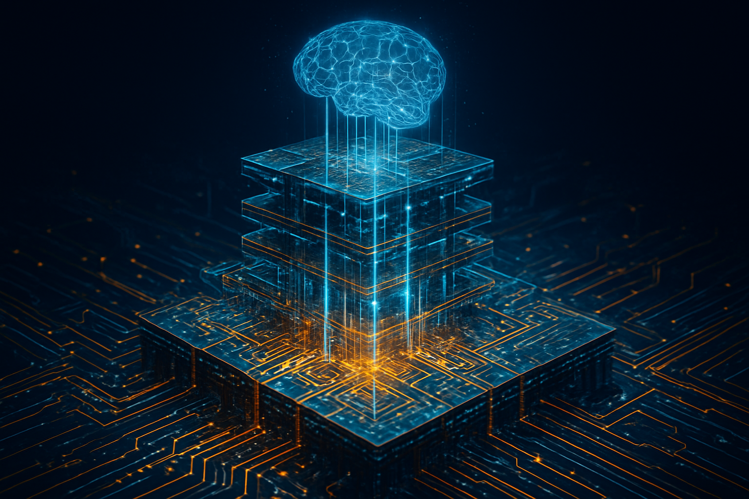
The Death of the Monolith and the Rise of "More than Moore"
The wider significance of 3D-IC packaging lies in its role as the savior of computational scaling. As we enter late 2025, the industry has largely accepted that "Moore's Law" in its traditional sense—doubling transistor density every two years on a single chip—is dead. In its place is the "More than Moore" era, where performance gains are driven by Heterogeneous Integration. This allows designers to use the most expensive 2nm or 3nm nodes for critical compute cores while using cheaper, more mature nodes for I/O and analog components, all unified in a single high-performance package.
This transition has profound implications for the AI landscape. It has enabled the creation of chips with over 200 billion transistors, a feat that would have been economically and physically impossible five years ago. However, it also raises concerns about the "Packaging Wall." As packages become larger and more complex, the risk of a single defect ruining a massive, expensive multi-die system increases. This has led to a renewed focus on "Known Good Die" (KGD) testing and sophisticated AI-driven inspection tools to ensure yields remain viable.
Comparatively, this milestone is being viewed as the "multicore moment" for the 2020s. Just as the shift to multicore CPUs saved the PC industry from the "Power Wall" in the mid-2000s, 3D-IC packaging is saving the AI industry from the "Reticle Wall." It is a fundamental architectural shift that will define the next decade of hardware, moving us toward a future where the "computer" is no longer a collection of chips on a board, but a single, massive, three-dimensional system-on-package.
The Future: Glass, Light, and HBM4
Looking ahead to 2026 and beyond, the roadmap for advanced packaging is even more radical. The next major frontier is the transition from organic substrates to glass substrates. Intel is currently leading this charge, aiming for mass production in 2026. Glass offers superior flatness and thermal stability, which will be essential as packages grow to 120x120mm and beyond. TSMC and Samsung (OTC: SSNLF) are also fast-tracking their glass R&D to compete in what is expected to be a trillion-transistor-per-package era by 2030.
Another imminent breakthrough is the integration of Optical Interconnects or Silicon Photonics directly into the package. TSMC’s COUPE (Compact Universal Photonic Engine) technology is expected to debut in 2026, replacing copper wires with light for chip-to-chip communication. This will drastically reduce the power required for data movement, which is currently one of the biggest overheads in AI training. Furthermore, the upcoming HBM4 standard will introduce "Active Base Dies," where the memory stack is bonded directly onto a logic die manufactured on an advanced node, effectively merging memory and compute into a single vertical unit.
A New Chapter in Silicon History
The story of AI in 2025 is increasingly a story of advanced packaging. What was once a mundane step at the end of the manufacturing process has become the primary theater of innovation and geopolitical competition. The success of CoWoS and SoIC has proved that the future of silicon is not just about getting smaller, but about getting smarter in how we stack and connect the building blocks of intelligence.
As we look toward 2026, the key takeaways are clear: packaging is the new bottleneck, heterogeneous integration is the new standard, and the "Systems Foundry" is the new business model. For investors and tech enthusiasts alike, the metrics to watch are no longer just nanometers, but interconnect density, bond pitch, and CoWoS wafer starts. The "Silicon Age" is entering its third dimension, and the companies that master this vertical frontier will be the ones that define the future of artificial intelligence.
This content is intended for informational purposes only and represents analysis of current AI developments.
TokenRing AI delivers enterprise-grade solutions for multi-agent AI workflow orchestration, AI-powered development tools, and seamless remote collaboration platforms. For more information, visit https://www.tokenring.ai/.