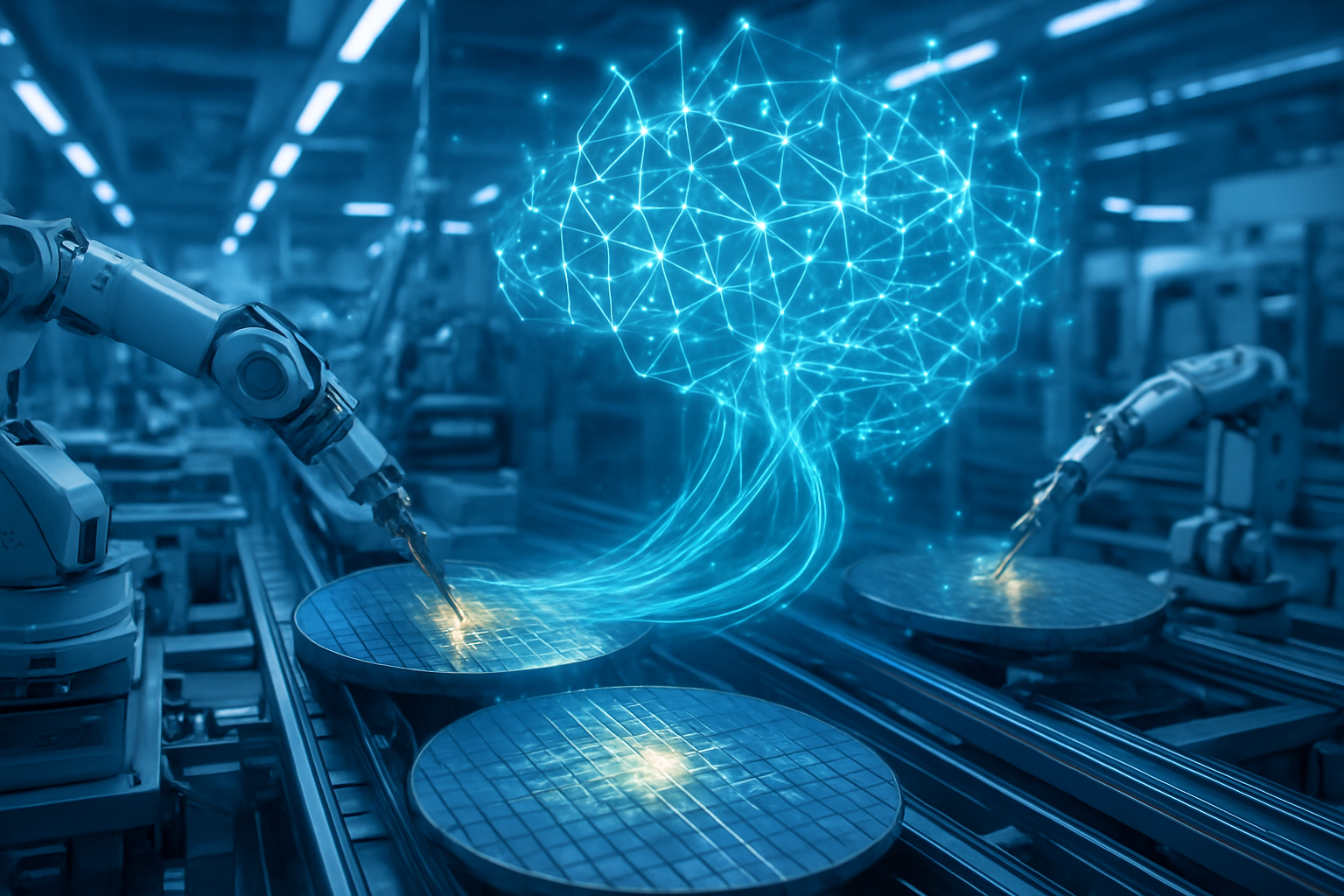
Tag: Semiconductors

  • Ricursive Intelligence Unleashes Frontier AI Lab to Revolutionize Chip Design and Chart Course for Superintelligence

    Ricursive Intelligence Unleashes Frontier AI Lab to Revolutionize Chip Design and Chart Course for Superintelligence

    San Francisco, CA – December 2, 2025 – In a move set to redefine the landscape of artificial intelligence and semiconductor innovation, Ricursive Intelligence today announced the official launch of its Frontier AI Lab. With a substantial $35 million in seed funding, the nascent company is embarking on an ambitious mission: to transform semiconductor design through advanced AI and accelerate humanity's path toward artificial superintelligence (ASI). This launch marks a significant step in the convergence of AI and hardware, promising to unlock unprecedented capabilities in future AI chips.

    The new lab is poised to tackle the complex challenges of modern chip architecture, leveraging a novel approach centered on "recursive intelligence." This paradigm envisions AI systems that continuously learn, adapt, and self-optimize by applying their own rules and procedures, leading to a dynamic and evolving design process for the next generation of computing hardware. The implications for both the efficiency of AI development and the power of future intelligent systems are profound, signaling a potential paradigm shift in how we conceive and build advanced AI.

    The Dawn of Recursive Chip Design: A Technical Deep Dive

    Ricursive Intelligence's core technical innovation lies in applying the principles of recursive intelligence directly to the intricate domain of semiconductor design. Unlike traditional Electronic Design Automation (EDA) tools that rely on predefined algorithms and human-guided iterations, Ricursive's AI systems are designed to autonomously refine chip architectures, optimize layouts, and identify efficiencies through a continuous feedback loop. This self-improving process aims to deconstruct complex design problems into manageable sub-problems, enhancing efficiency and innovation over time. The goal is to move beyond static AI models to adaptive, real-time AI learning that can dynamically evolve and self-optimize, ultimately targeting advanced nodes like 2nm technology for significant gains in power efficiency and performance.

    This approach dramatically differs from previous methodologies by embedding intelligence directly into the design process itself, allowing the AI to learn from its own design outcomes and iteratively improve. While generative AI tools and machine learning algorithms are already being explored in semiconductor design to automate tasks and optimize certain parameters, Ricursive's recursive intelligence takes this a step further by enabling self-referential improvement and autonomous adaptation. This could lead to a significant reduction in design cycles, lower costs, and the creation of more powerful and specialized AI accelerators tailored for future superintelligence.

    Initial reactions from the broader AI research community, while not yet specific to Ricursive Intelligence, highlight both excitement and caution. Experts generally recognize the immense potential of frontier AI labs and recursive AI in accelerating capabilities and potentially ushering in superhuman machines. The ability of AI to continuously grow, adapt, and innovate, developing a form of "synthetic intuition," is seen as transformative. However, alongside the enthusiasm, there are significant discussions about the critical need for robust governance, ethical frameworks, and safety measures, especially as AI systems gain the ability to rewrite their own rules and mental models. The concern about "safetywashing"—where alignment efforts might inadvertently advance capabilities without fully addressing long-term risks—remains a prevalent topic.

    Reshaping the AI and Tech Landscape

    The launch of Ricursive Intelligence's Frontier AI Lab carries significant implications for AI companies, tech giants, and startups alike. Companies heavily invested in AI hardware, such as NVIDIA (NASDAQ: NVDA), Intel (NASDAQ: INTC), and AMD (NASDAQ: AMD), stand to both benefit and face new competitive pressures. If Ricursive Intelligence successfully develops more efficient and powerful AI-designed chips, it could either become a crucial partner for these companies, providing advanced design methodologies, or emerge as a formidable competitor in specialized AI chip development. Tech giants like Google (NASDAQ: GOOGL), Microsoft (NASDAQ: MSFT), and Amazon (NASDAQ: AMZN), all with substantial AI research and cloud infrastructure divisions, could leverage such advancements to enhance their own AI models and services, potentially gaining significant competitive advantages in performance and cost-efficiency for their data centers and edge devices.

    For major AI labs, including those within these tech giants and independent entities like OpenAI and Anthropic, Ricursive Intelligence's work could accelerate their own AI development, particularly in training larger, more complex models that require cutting-edge hardware. The potential disruption to existing products and services could be substantial if AI-designed chips offer a significant leap in performance-per-watt or cost-effectiveness. This could force established players to rapidly adopt new design paradigms or risk falling behind. Startups focusing on niche AI hardware or specialized AI applications might find new opportunities through access to more advanced, AI-optimized silicon, or face increased barriers to entry if the cost of developing such sophisticated chips becomes prohibitive without recursive AI assistance. Ricursive Intelligence's early market positioning, backed by a significant seed round from Sequoia, places it as a key player to watch in the evolving AI hardware race.

    Wider Significance and the Path to ASI

    Ricursive Intelligence's endeavor fits squarely into the broader AI landscape as a critical step in the ongoing quest for more capable and autonomous AI systems. It represents a tangible effort to bridge the gap between theoretical AI advancements and the physical hardware required to realize them, pushing the boundaries of what's possible in computational power. This development aligns with the trend of "AI for AI," where AI itself is used to accelerate the research and development of more advanced AI.

    The impacts could be far-reaching, extending beyond just faster chips. More efficient AI-designed semiconductors could reduce the energy footprint of large AI models, addressing a growing environmental concern. Furthermore, the acceleration toward artificial superintelligence, while a long-term goal, raises significant societal questions about control, ethics, and the future of work. Potential concerns, as echoed by the broader AI community, include the challenges of ensuring alignment with human values, preventing unintended consequences from self-improving systems, and managing the economic and social disruptions that ASI could bring. This milestone evokes comparisons to previous AI breakthroughs like the development of deep learning or the advent of large language models, but with the added dimension of AI designing its own foundational hardware, it suggests a new level of autonomy and potential for exponential growth.

    The Road Ahead: Future Developments and Challenges

    In the near term, experts predict that Ricursive Intelligence will focus on demonstrating the tangible benefits of recursive AI in specific semiconductor design tasks, such as optimizing particular chip components or accelerating verification processes. The immediate challenge will be to translate the theoretical advantages of recursive intelligence into demonstrable improvements over conventional EDA tools, particularly in terms of design speed, efficiency, and the ultimate performance of the resulting silicon. We can expect to see early prototypes and proof-of-concept chips that showcase the AI's ability to innovate in chip architecture.

    Longer term, the potential applications are vast. Recursive AI could lead to the development of highly specialized AI accelerators perfectly tuned for specific tasks, enabling breakthroughs in fields like drug discovery, climate modeling, and personalized medicine. The ultimate goal of accelerating artificial superintelligence suggests a future where AI systems can design hardware so advanced that it facilitates their own further development, creating a virtuous cycle of intelligence amplification. However, significant challenges remain, including the computational cost of training and running recursive AI systems, the need for massive datasets for design optimization, and the crucial task of ensuring the safety and alignment of increasingly autonomous design processes. Experts predict a future where AI-driven design becomes the norm, but the journey will require careful navigation of technical hurdles and profound ethical considerations.

    A New Epoch in AI Development

    The launch of Ricursive Intelligence's Frontier AI Lab marks a pivotal moment in AI history, signaling a concerted effort to merge the frontier of artificial intelligence with the foundational technology of semiconductors. The key takeaway is the introduction of "recursive intelligence" as a methodology not just for AI development, but for the very creation of the hardware that powers it. This development's significance lies in its potential to dramatically shorten the cycle of innovation for AI chips, potentially leading to an unprecedented acceleration in AI capabilities.

    As we assess this development, it's clear that Ricursive Intelligence is positioning itself at the nexus of two critical technological frontiers. The long-term impact could be transformative, fundamentally altering how we design, build, and interact with AI systems. The pursuit of artificial superintelligence, underpinned by self-improving hardware design, raises both immense promise and significant questions for humanity. In the coming weeks and months, the tech world will be closely watching for further technical details, early benchmarks, and the initial strategic partnerships that Ricursive Intelligence forms, as these will provide crucial insights into the trajectory and potential impact of this ambitious new venture.


    This content is intended for informational purposes only and represents analysis of current AI developments.

    TokenRing AI delivers enterprise-grade solutions for multi-agent AI workflow orchestration, AI-powered development tools, and seamless remote collaboration platforms.
    For more information, visit https://www.tokenring.ai/.

  • The Silicon Brains: Why AI’s Future is Forged in Advanced Semiconductors – Top 5 Stocks to Watch

    The Silicon Brains: Why AI’s Future is Forged in Advanced Semiconductors – Top 5 Stocks to Watch

    The relentless march of artificial intelligence (AI) is reshaping industries, redefining possibilities, and demanding an unprecedented surge in computational power. At the heart of this revolution lies a symbiotic relationship with the semiconductor industry, where advancements in chip technology directly fuel AI's capabilities, and AI, in turn, drives the innovation cycle for new silicon. As of December 1, 2025, this intertwined destiny presents a compelling investment landscape, with leading semiconductor companies emerging as the foundational architects of the AI era.

    This dynamic interplay has made the demand for specialized, high-performance, and energy-efficient chips more critical than ever. From training colossal neural networks to enabling real-time AI at the edge, the semiconductor industry is not merely a supplier but a co-creator of AI's future. Understanding this crucial connection is key to identifying the companies poised for significant growth in the years to come.

    The Unbreakable Bond: How Silicon Powers Intelligence and Intelligence Refines Silicon

    The intricate dance between AI and semiconductors is a testament to technological co-evolution. AI's burgeoning complexity, particularly with the advent of large language models (LLMs) and sophisticated machine learning algorithms, places immense demands on processing power, memory bandwidth, and energy efficiency. This insatiable appetite has pushed semiconductor manufacturers to innovate at an accelerated pace, leading to the development of specialized processors like Graphics Processing Units (GPUs), Tensor Processing Units (TPUs), Neural Processing Units (NPUs), and Application-Specific Integrated Circuits (ASICs), all meticulously engineered to handle AI workloads with unparalleled performance. Innovations in advanced lithography, 3D chip stacking, and heterogeneous integration are direct responses to AI's escalating requirements.

    Conversely, these cutting-edge semiconductors are the very bedrock upon which advanced AI systems are built. They provide the computational muscle necessary for complex calculations and data processing at speeds previously unimaginable. Advances in process nodes, such as 3nm and 2nm technology, allow for an exponentially greater number of transistors to be packed onto a single chip, translating directly into the performance gains crucial for developing and deploying sophisticated AI. Moreover, semiconductors are pivotal in democratizing AI, extending its reach beyond data centers to "edge" devices like smartphones, autonomous vehicles, and IoT sensors, where real-time, local processing with minimal power consumption is paramount.

    The relationship isn't one-sided; AI itself is becoming an indispensable tool within the semiconductor industry. AI-driven software is revolutionizing chip design by automating intricate layout generation, logic synthesis, and verification processes, significantly reducing development cycles and time-to-market. In manufacturing, AI-powered visual inspection systems can detect microscopic defects with far greater accuracy than human operators, boosting yield and minimizing waste. Furthermore, AI plays a critical role in real-time process control, optimizing manufacturing parameters, and enhancing supply chain management through advanced demand forecasting and inventory optimization. Initial reactions from the AI research community and industry experts consistently highlight this as a "ten-year AI cycle," emphasizing the long-term, foundational nature of this technological convergence.

    Navigating the AI-Semiconductor Nexus: Companies Poised for Growth

    The profound synergy between AI and semiconductors has created a fertile ground for companies at the forefront of this convergence. Several key players are not just riding the wave but actively shaping the future of AI through their silicon innovations. As of late 2025, these companies stand out for their market dominance, technological prowess, and strategic positioning.

    NVIDIA (NASDAQ: NVDA) remains the undisputed titan in AI chips. Its GPUs and AI accelerators, particularly the A100 Tensor Core GPU and the newer Blackwell Ultra architecture (like the GB300 NVL72 rack-scale system), are the backbone of high-performance AI training and inference. NVIDIA's comprehensive ecosystem, anchored by its CUDA software platform, is deeply embedded in enterprise and sovereign AI initiatives globally, making it a default choice for many AI developers and data centers. The company's leadership in accelerated and AI computing directly benefits from the multi-year build-out of "AI factories," with analysts projecting substantial revenue growth driven by sustained demand for its cutting-edge chips.

    Advanced Micro Devices (AMD) (NASDAQ: AMD) has emerged as a formidable challenger to NVIDIA, offering a robust portfolio of CPU, GPU, and AI accelerator products. Its EPYC processors deliver strong performance for data centers, including those running AI workloads. AMD's MI300 series is specifically designed for AI training, with a roadmap extending to the MI400 "Helios" racks for hyperscale applications, leveraging TSMC's advanced 3nm process. The company's ROCm software stack is also gaining traction as a credible, open-source alternative to CUDA, further strengthening its competitive stance. AMD views the current period as a "ten-year AI cycle," making significant strategic investments to capture a larger share of the AI chip market.

    Intel (NASDAQ: INTC), a long-standing leader in CPUs, is aggressively expanding its footprint in AI accelerators. Unlike many of its competitors, Intel operates its own foundries, providing a distinct advantage in manufacturing control and supply chain resilience. Intel's Gaudi AI Accelerators, notably the Gaudi 3, are designed for deep learning training and inference in data centers, directly competing with offerings from NVIDIA and AMD. Furthermore, Intel is integrating AI acceleration capabilities into its Xeon processors for data centers and edge computing, aiming for greater efficiency and cost-effectiveness in LLM operations. The company's foundry division is actively manufacturing chips for external clients, signaling its ambition to become a major contract manufacturer in the AI era.

    Taiwan Semiconductor Manufacturing Company (TSMC) (NYSE: TSM) is arguably the most critical enabler of the AI revolution, serving as the world's largest dedicated independent semiconductor foundry. TSMC manufactures the advanced chips for virtually all leading AI chip designers, including Apple, NVIDIA, and AMD. Its technological superiority in advanced process nodes (e.g., 3nm and below) is indispensable for producing the high-performance, energy-efficient chips demanded by AI systems. TSMC itself leverages AI in its operations to classify wafer defects and generate predictive maintenance charts, thereby enhancing yield and reducing downtime. The company projects its AI-related revenue to grow at a compound annual rate of 40% through 2029, underscoring the profound impact of AI demand on its business.

    Qualcomm (NASDAQ: QCOM) is a pioneer in mobile system-on-chip (SoC) architectures and a leader in edge AI. Its Snapdragon AI processors are optimized for on-device AI in smartphones, autonomous vehicles, and various IoT devices. These chips combine high performance with low power consumption, enabling AI processing directly on devices without constant cloud connectivity. Qualcomm's strategic focus on on-device AI is crucial as AI extends beyond data centers to real-time, local applications, driving innovation in areas like personalized AI assistants, advanced robotics, and intelligent sensor networks. The company's strengths in processing power, memory solutions, and networking capabilities position it as a key player in the expanding AI landscape.

    The Broader Implications: Reshaping the Global Tech Landscape

    The profound link between AI and semiconductors extends far beyond individual company performance, fundamentally reshaping the broader AI landscape and global technological trends. This symbiotic relationship is the primary driver behind the acceleration of AI development, enabling increasingly sophisticated models and diverse applications that were once confined to science fiction. The concept of "AI factories" – massive data centers dedicated to training and deploying AI models – is rapidly becoming a reality, fueled by the continuous flow of advanced silicon.

    The impacts are ubiquitous, touching every sector from healthcare and finance to manufacturing and entertainment. AI-powered diagnostics, personalized medicine, autonomous logistics, and hyper-realistic content creation are all direct beneficiaries of this technological convergence. However, this rapid advancement also brings potential concerns. The immense demand for cutting-edge chips raises questions about supply chain resilience, geopolitical stability, and the environmental footprint of large-scale AI infrastructure, particularly concerning energy consumption. The race for AI supremacy is also intensifying, drawing comparisons to previous technological gold rushes like the internet boom and the mobile revolution, but with potentially far greater societal implications.

    This era represents a significant milestone, a foundational shift akin to the invention of the microprocessor itself. The ability to process vast amounts of data at unprecedented speeds is not just an incremental improvement; it's a paradigm shift that will unlock entirely new classes of intelligent systems and applications.

    The Road Ahead: Future Developments and Uncharted Territories

    The horizon for AI and semiconductor development is brimming with anticipated breakthroughs and transformative applications. In the near term, we can expect the continued miniaturization of process nodes, pushing towards 2nm and even 1nm technologies, which will further enhance chip performance and energy efficiency. Novel chip architectures, including specialized AI accelerators beyond current GPU designs and advancements in neuromorphic computing, which mimics the structure and function of the human brain, are also on the horizon. These innovations promise to deliver even greater computational power for AI while drastically reducing energy consumption.

    Looking further out, the potential applications and use cases are staggering. Fully autonomous systems, from self-driving cars to intelligent robotic companions, will become more prevalent and capable. Personalized AI, tailored to individual needs and preferences, will seamlessly integrate into daily life, offering proactive assistance and intelligent insights. Advanced robotics and industrial automation, powered by increasingly intelligent edge AI, will revolutionize manufacturing and logistics. However, several challenges need to be addressed, including the continuous demand for greater power efficiency, the escalating costs associated with advanced chip manufacturing, and the global talent gap in AI research and semiconductor engineering. Experts predict that the "AI factory" model will continue to expand, leading to a proliferation of specialized AI hardware and a deepening integration of AI into every facet of technology.

    A New Era Forged in Silicon and Intelligence

    In summary, the current era marks a pivotal moment where the destinies of artificial intelligence and semiconductor technology are inextricably linked. The relentless pursuit of more powerful, efficient, and specialized chips is the engine driving AI's exponential growth, enabling breakthroughs that are rapidly transforming industries and societies. Conversely, AI is not only consuming these advanced chips but also actively contributing to their design and manufacturing, creating a self-reinforcing cycle of innovation.

    This development is not merely significant; it is foundational for the next era of technological advancement. The companies highlighted – NVIDIA (NASDAQ: NVDA), Advanced Micro Devices (AMD) (NASDAQ: AMD), Intel (NASDAQ: INTC), Taiwan Semiconductor Manufacturing Company (TSMC) (NYSE: TSM), and Qualcomm (NASDAQ: QCOM) – are at the vanguard of this revolution, strategically positioned to capitalize on the surging demand for AI-enabling silicon. Their continuous innovation and market leadership make them crucial players to watch in the coming weeks and months. The long-term impact of this convergence will undoubtedly reshape global economies, redefine human-computer interaction, and usher in an age of pervasive intelligence.


    This content is intended for informational purposes only and represents analysis of current AI developments.

    TokenRing AI delivers enterprise-grade solutions for multi-agent AI workflow orchestration, AI-powered development tools, and seamless remote collaboration platforms.
    For more information, visit https://www.tokenring.ai/.

  • Beyond Silicon: The Dawn of a New Era in Semiconductor Fabrication

    Beyond Silicon: The Dawn of a New Era in Semiconductor Fabrication

    The foundational material of the modern digital age, silicon, is rapidly approaching its inherent physical and performance limitations, heralding a pivotal shift in semiconductor fabrication. As the relentless demand for faster, smaller, and more energy-efficient chips intensifies, the tech industry is turning its gaze towards a promising new generation of materials. Gallium Nitride (GaN), Silicon Carbide (SiC), and two-dimensional (2D) materials like graphene are emerging as critical contenders to augment or even replace silicon, promising to unlock unprecedented advancements in computing power, energy efficiency, and miniaturization that are vital for the future of artificial intelligence, high-performance computing, and advanced electronics.

    This paradigm shift is not merely an incremental improvement but a fundamental re-evaluation of the building blocks of technology. The immediate significance of these emerging materials lies in their ability to shatter silicon's long-standing barriers, offering solutions to challenges that silicon simply cannot overcome. From powering the next generation of electric vehicles to enabling ultra-fast 5G/6G communication networks and creating more efficient data centers, these novel materials are poised to redefine what's possible in the world of semiconductors.

    The Technical Edge: Unpacking the Power of Next-Gen Materials

    Silicon's dominance for decades has been due to its abundance, excellent semiconductor properties, and well-established manufacturing processes. However, as transistors shrink to near-atomic scales, silicon faces insurmountable hurdles in miniaturization, power consumption, heat dissipation, and breakdown at high temperatures and voltages. This is where wide-bandgap (WBG) semiconductors like GaN and SiC, along with revolutionary 2D materials, step in, offering distinct advantages that silicon cannot match.

    Gallium Nitride (GaN), with a bandgap of 3.4 electron volts (eV) compared to silicon's 1.1 eV, is a game-changer for high-frequency and high-power applications. Its high electron mobility and saturation velocity allow GaN devices to switch up to 100 times faster than silicon, drastically reducing energy losses and boosting efficiency, particularly in power conversion systems. This translates to smaller, lighter, and more efficient power adapters (like those found in fast chargers), as well as significant energy savings in data centers and wireless infrastructure. GaN's superior thermal conductivity also means less heat generation and more effective dissipation, crucial for compact and reliable devices. The AI research community and industry experts have enthusiastically embraced GaN, recognizing its immediate impact on power electronics and its potential to enable more efficient AI hardware by reducing power overhead.

    Silicon Carbide (SiC), another WBG semiconductor with a bandgap of 3.3 eV, excels in extreme operating conditions. SiC devices can withstand significantly higher voltages (up to 10 times higher breakdown field strength than silicon) and temperatures, making them exceptionally robust for harsh environments. Its thermal conductivity is 3-4 times greater than silicon, which is vital for managing heavy loads in high-power applications such as electric vehicle (EV) inverters, solar inverters, and industrial motor drives. SiC semiconductors can reduce energy losses by up to 50% during power conversion, directly contributing to increased range and faster charging times for EVs. The automotive industry, in particular, has been a major driver for SiC adoption, with leading manufacturers integrating SiC into their next-generation electric powertrains, marking a clear departure from silicon-based power modules.

    Beyond WBG materials, two-dimensional (2D) materials like graphene and molybdenum disulfide (MoS2) represent the ultimate frontier in miniaturization. Graphene, a single layer of carbon atoms, boasts extraordinary electron mobility—up to 100 times that of silicon—and exceptional thermal conductivity, making it ideal for ultra-fast transistors and interconnects. While early graphene lacked an intrinsic bandgap, recent breakthroughs in engineering semiconducting graphene and the discovery of other 2D materials like MoS2 (with a stable bandgap nearly twice that of silicon) have reignited excitement. These atomically thin materials are paramount for pushing Moore's Law further, enabling novel 3D device architectures that can be stacked without significant performance degradation. The ability to create flexible and transparent electronics also opens doors for new form factors in wearable technology and advanced displays, garnering significant attention from leading research institutions and semiconductor giants for their potential to overcome silicon's ultimate scaling limits.

    Corporate Race: The Strategic Imperative for Tech Giants and Startups

    The shift towards non-silicon materials is igniting a fierce competitive race among semiconductor companies, tech giants, and innovative startups. Companies heavily invested in power electronics, automotive, and telecommunications stand to benefit immensely. Infineon Technologies AG (XTRA: IFX), STMicroelectronics N.V. (NYSE: STM), and ON Semiconductor Corporation (NASDAQ: ON) are leading the charge in SiC and GaN manufacturing, aggressively expanding production capabilities and R&D to meet surging demand from the electric vehicle and industrial sectors. These companies are strategically positioning themselves to dominate the high-growth markets for power management and conversion, where SiC and GaN offer unparalleled performance.

    For major AI labs and tech companies like NVIDIA Corporation (NASDAQ: NVDA), Intel Corporation (NASDAQ: INTC), and Taiwan Semiconductor Manufacturing Company Limited (NYSE: TSM), the implications are profound. While their primary focus remains on silicon for general-purpose computing, the adoption of GaN and SiC in power delivery and high-frequency components will enable more efficient and powerful AI accelerators and data center infrastructure. Intel, for instance, has been actively researching 2D materials for future transistor designs, aiming to extend the capabilities of its processors beyond silicon's physical limits. The ability to integrate these novel materials could lead to breakthroughs in energy efficiency for AI training and inference, significantly reducing operational costs and environmental impact. Startups specializing in GaN and SiC device fabrication, such as Navitas Semiconductor Corporation (NASDAQ: NVTS) and Wolfspeed, Inc. (NYSE: WOLF), are experiencing rapid growth, disrupting traditional silicon-centric supply chains with their specialized expertise and advanced manufacturing processes.

    The potential disruption to existing products and services is substantial. As GaN and SiC become more cost-effective and widespread, they will displace silicon in a growing number of applications where performance and efficiency are paramount. This could lead to a re-calibration of market share in power electronics, with companies that quickly adapt to these new material platforms gaining a significant strategic advantage. For 2D materials, the long-term competitive implications are even greater, potentially enabling entirely new categories of devices and computing paradigms that are currently impossible with silicon, pushing the boundaries of miniaturization and functionality. Companies that invest early and heavily in the research and development of these advanced materials are setting themselves up to define the next generation of technological innovation.

    A Broader Horizon: Reshaping the AI Landscape and Beyond

    The exploration of materials beyond silicon marks a critical juncture in the broader technological landscape, akin to previous monumental shifts in computing. This transition is not merely about faster chips; it underpins the continued advancement of artificial intelligence, edge computing, and sustainable energy solutions. The limitations of silicon have become a bottleneck for AI's insatiable demand for computational power and energy efficiency. Novel materials directly address this by enabling processors that run cooler, consume less power, and operate at higher frequencies, accelerating the development of more complex neural networks and real-time AI applications.

    The impacts extend far beyond the tech industry. In terms of sustainability, the superior energy efficiency of GaN and SiC devices can significantly reduce the carbon footprint of data centers, electric vehicles, and power grids. For instance, the widespread adoption of GaN in data center power supplies could lead to substantial reductions in global energy consumption and CO2 emissions, addressing pressing environmental concerns. The ability of 2D materials to enable extreme miniaturization and flexible electronics could also lead to advancements in medical implants, ubiquitous sensing, and personalized health monitoring, integrating technology more seamlessly into daily life.

    Potential concerns revolve around the scalability of manufacturing these new materials, their cost-effectiveness compared to silicon (at least initially), and the establishment of robust supply chains. While significant progress has been made, bringing these technologies to mass production with the same consistency and cost as silicon remains a challenge. However, the current momentum and investment indicate a strong commitment to overcoming these hurdles. This shift can be compared to the transition from vacuum tubes to transistors or from discrete components to integrated circuits—each marked a fundamental change that propelled technology forward by orders of magnitude. The move beyond silicon is poised to be another such transformative milestone, enabling the next wave of innovation across virtually every sector.

    The Road Ahead: Future Developments and Expert Predictions

    The trajectory for emerging semiconductor materials is one of rapid evolution and expanding applications. In the near term, we can expect to see continued widespread adoption of GaN and SiC in power electronics, particularly in electric vehicles, fast chargers, and renewable energy systems. The focus will be on improving manufacturing yields, reducing costs, and enhancing the reliability and performance of GaN and SiC devices. Experts predict a significant increase in the market share for these WBG semiconductors, with SiC dominating high-power, high-voltage applications and GaN excelling in high-frequency, medium-power domains.

    Longer term, the potential of 2D materials is immense. Research into graphene and other transition metal dichalcogenides (TMDs) will continue to push the boundaries of transistor design, aiming for atomic-scale devices that can operate at unprecedented speeds with minimal power consumption. The integration of 2D materials into existing silicon fabrication processes, potentially through monolithic 3D integration, is a key area of focus. This could lead to hybrid chips that leverage the best properties of both silicon and 2D materials, enabling novel architectures for quantum computing, neuromorphic computing, and ultra-dense memory. Challenges that need to be addressed include scalable and defect-free growth of large-area 2D materials, effective doping strategies, and reliable contact formation at the atomic scale.

    Experts predict that the next decade will witness a diversification of semiconductor materials, moving away from a silicon-monopoly towards a more specialized approach where different materials are chosen for their optimal properties in specific applications. We can anticipate breakthroughs in new material combinations, advanced packaging techniques for heterogeneous integration, and the development of entirely new device architectures. The ultimate goal is to enable a future where computing is ubiquitous, intelligent, and sustainable, with novel materials playing a crucial role in realizing this vision.

    A New Foundation for the Digital Age

    The journey beyond silicon represents a fundamental re-imagining of the building blocks of our digital world. The emergence of gallium nitride, silicon carbide, and 2D materials like graphene is not merely an incremental technological upgrade; it is a profound shift that promises to redefine the limits of performance, efficiency, and miniaturization in semiconductor devices. The key takeaway is clear: silicon's reign as the sole king of semiconductors is drawing to a close, making way for a multi-material future where specialized materials unlock unprecedented capabilities across diverse applications.

    This development is of immense significance in AI history, as it directly addresses the physical constraints that could otherwise impede the continued progress of artificial intelligence. By enabling more powerful, efficient, and compact hardware, these novel materials will accelerate advancements in machine learning, deep learning, and edge AI, allowing for more sophisticated and pervasive intelligent systems. The long-term impact will be felt across every industry, from enabling smarter grids and more sustainable energy solutions to revolutionizing transportation, healthcare, and communication.

    In the coming weeks and months, watch for further announcements regarding manufacturing scale-up for GaN and SiC, particularly from major players in the automotive and power electronics sectors. Keep an eye on research breakthroughs in 2D materials, especially concerning their integration into commercial fabrication processes and the development of functional prototypes. The race to master these new materials is on, and the implications for the future of technology are nothing short of revolutionary.


    This content is intended for informational purposes only and represents analysis of current AI developments.

    TokenRing AI delivers enterprise-grade solutions for multi-agent AI workflow orchestration, AI-powered development tools, and seamless remote collaboration platforms.
    For more information, visit https://www.tokenring.ai/.

  • Advanced Packaging: The Unsung Hero Propelling AI’s Next Revolution

    Advanced Packaging: The Unsung Hero Propelling AI’s Next Revolution

    In an era where Artificial Intelligence (AI) is rapidly redefining industries and daily life, the relentless pursuit of faster, more efficient, and more powerful computing hardware has become paramount. While much attention focuses on groundbreaking algorithms and software innovations, a quieter revolution is unfolding beneath the surface of every cutting-edge AI chip: advanced semiconductor packaging. Technologies like 3D stacking, chiplets, and fan-out packaging are no longer mere afterthoughts in chip manufacturing; they are the critical enablers boosting the performance, power efficiency, and cost-effectiveness of semiconductors, fundamentally shaping the future of high-performance computing (HPC) and AI hardware.

    These innovations are steering the semiconductor industry beyond the traditional confines of 2D integration, where components are laid out side-by-side on a single plane. As Moore's Law—the decades-old prediction that the number of transistors on a microchip doubles approximately every two years—faces increasing physical and economic limitations, advanced packaging has emerged as the essential pathway to continued performance scaling. By intelligently integrating and interconnecting components in three dimensions and modular forms, these technologies are unlocking unprecedented capabilities, allowing AI models to grow in complexity and speed, from the largest data centers to the smallest edge devices.

    Beyond the Monolith: Technical Innovations Driving AI Hardware

    The shift to advanced packaging marks a profound departure from the monolithic chip design of the past, introducing intricate architectures that maximize data throughput and minimize latency.

    3D Stacking (3D ICs)

    3D stacking involves vertically integrating multiple semiconductor dies (chips) within a single package, interconnected by ultra-short, high-bandwidth connections. The most prominent of these are Through-Silicon Vias (TSVs), which are vertical electrical connections passing directly through the silicon layers, or advanced copper-to-copper (Cu-Cu) hybrid bonding, which creates molecular-level connections. This vertical integration dramatically reduces the physical distance data must travel, leading to significantly faster data transfer speeds, improved performance, and enhanced power efficiency due to shorter interconnects and lower capacitance. For AI, 3D ICs can offer I/O density increases of up to 100x and energy-per-bit transfer reductions of up to 30x. This is particularly crucial for High Bandwidth Memory (HBM), which utilizes 3D stacking with TSVs to achieve unprecedented memory bandwidth, a vital component for data-intensive AI workloads. The AI research community widely acknowledges 3D stacking as indispensable for overcoming the "memory wall" bottleneck, providing the necessary bandwidth and low latency for complex machine learning models.

    Chiplets

    Chiplets represent a modular approach, breaking down a large, complex chip into smaller, specialized dies, each performing a specific function (e.g., CPU, GPU, memory, I/O, AI accelerator). These pre-designed and pre-tested chiplets are then interconnected within a single package, often using 2.5D integration where they are mounted side-by-side on a silicon interposer, or even 3D integration. This modularity offers several advantages over traditional monolithic System-on-Chip (SoC) designs: improved manufacturing yields (as defects on smaller chiplets are less costly), greater design flexibility, and the ability to mix and match components from various process nodes to optimize for performance, power, and cost. Standards like the Universal Chiplet Interconnect Express (UCIe) are emerging to facilitate interoperability between chiplets from different vendors. Industry experts view chiplets as redefining the future of AI processing, providing a scalable and customizable approach essential for generative AI, high-performance computing, and edge AI systems.

    Fan-Out Packaging (FOWLP/FOPLP)

    Fan-out Wafer-Level Packaging (FOWLP) is an advanced technique where the connection points (I/Os) are redistributed from the chip's periphery over a larger area, extending beyond the original die footprint. After dicing, individual dies are repositioned on a carrier wafer or panel, molded, and then connected via Redistribution Layers (RDLs) and solder balls. This substrateless or substrate-light design enables ultra-thin and compact packages, often reducing package size by 40%, while supporting a higher number of I/Os. FOWLP also offers improved thermal and electrical performance due to shorter electrical paths and better heat spreading. Panel-Level Packaging (FOPLP) further enhances cost-efficiency by processing on larger, square panels instead of round wafers. FOWLP is recognized as a game-changer, providing high-density packaging and excellent performance for applications in 5G, automotive, AI, and consumer electronics, as exemplified by Apple's (NASDAQ: AAPL) use of TSMC's (NYSE: TSM) Integrated Fan-Out (InFO) technology in its A-series chips.

    Reshaping the AI Competitive Landscape

    The strategic importance of advanced packaging is profoundly impacting AI companies, tech giants, and startups, creating new competitive dynamics and strategic advantages.

    Major tech giants are at the forefront of this transformation. NVIDIA (NASDAQ: NVDA), a leader in AI accelerators, heavily relies on advanced packaging, particularly TSMC's CoWoS (Chip-on-Wafer-on-Substrate) technology, for its high-performance GPUs like the Hopper H100 and upcoming Blackwell chips. NVIDIA's transition to CoWoS-L technology signifies the continuous demand for enhanced design and packaging flexibility for large AI chips. Intel (NASDAQ: INTC) is aggressively developing its own advanced packaging solutions, including Foveros (3D stacking) and EMIB (Embedded Multi-die Interconnect Bridge, a 2.5D technology). Intel's EMIB is gaining traction, with cloud service providers (CSPs) like Alphabet (NASDAQ: GOOGL) evaluating it for their custom AI accelerators (TPUs), driven by strong demand and a need for diversified packaging supply. This collaboration with partners like Amkor Technology (NASDAQ: AMKR) to scale EMIB production highlights the strategic importance of packaging expertise.

    Advanced Micro Devices (NASDAQ: AMD) has been a pioneer in chiplet-based CPUs and GPUs with its EPYC and Instinct lines, leveraging its Infinity Fabric interconnect, and is pushing 3D stacking with its 3D V-Cache technology. Samsung Electronics (KRX: 005930), a major player in memory, foundry, and packaging, offers its X-Cube technology for vertical stacking of logic and SRAM dies, presenting a strategic advantage with its integrated turnkey solutions.

    For AI startups, advanced packaging presents both opportunities and challenges. Chiplets, in particular, can lower entry barriers by reducing the need to design complex monolithic chips from scratch, allowing startups to integrate best-in-class IP and accelerate time-to-market with specialized AI accelerators. Companies like Mixx Technologies are innovating with optical interconnect systems using silicon photonics and advanced packaging. However, startups face challenges such as the high manufacturing complexity and cost of advanced packaging, thermal management issues, and the need for skilled labor.

    The competitive landscape is shifting, with packaging no longer a commodity but a strategic differentiator. Companies with strong access to advanced foundries (like TSMC and Intel Foundry) and packaging expertise gain a significant edge. Outsourced Semiconductor Assembly and Test (OSAT) vendors like Amkor Technology are becoming critical partners. The capacity crunch for leading advanced packaging technologies is prompting tech giants to diversify their supply chains, fostering competition and innovation. This evolution blurs traditional roles, with back-end design and packaging gaining immense value, pushing the industry towards system-level co-optimization. This disruption to traditional monolithic chip designs means that purely monolithic high-performance AI chips may become less competitive as multi-chip integration offers superior performance and cost efficiencies.

    A New Era for AI: Wider Significance and Future Implications

    Advanced packaging technologies represent a fundamental hardware-centric breakthrough for AI, akin to the advent of Graphics Processing Units (GPUs) in the mid-2000s, which provided the parallel processing power to catalyze the deep learning revolution. Just as GPUs enabled the training of previously intractable neural networks, advanced packaging provides the essential physical infrastructure to realize and deploy today's and tomorrow's sophisticated AI models at scale. It directly addresses the "memory wall" and other fundamental hardware bottlenecks, pushing past the limits of traditional silicon scaling into the "More than Moore" era, where performance gains are achieved through innovative integration.

    The overall impact on the AI landscape is profound: enhanced performance, improved power efficiency, miniaturization for edge AI, and unparalleled scalability and flexibility through chiplets. These advancements are crucial for handling the immense computational demands of Large Language Models (LLMs) and generative AI, enabling larger and more complex AI models.

    However, this transformation is not without its challenges. The increased power density from tightly integrated components exacerbates thermal management issues, demanding innovative cooling solutions. Manufacturing complexity, especially with hybrid bonding, increases the risk of defects and complicates yield management. Testing heterogeneous chiplet-based systems is also significantly more complex than monolithic chips, requiring robust testing protocols. The absence of universal chiplet testing standards and interoperability protocols also presents a challenge, though initiatives like UCIe are working to address this. Furthermore, the high capital investment for advanced packaging equipment and expertise can be substantial, and supply chain constraints, such as TSMC's advanced packaging capacity, remain a concern.

    Looking ahead, experts predict a dynamic future for advanced packaging, with AI at its core. Near-term advancements (1-5 years) include the widespread adoption of hybrid bonding for finer interconnect pitches, continued evolution of HBM with higher stacks, and improved TSV fabrication. Chiplets will see standardized interfaces and increasingly specialized AI chiplets, while fan-out packaging will move towards higher density, Panel-Level Packaging (FOPLP), and integration with glass substrates for enhanced thermal stability.

    Long-term (beyond 5 years), the industry anticipates logic-memory hybrids becoming mainstream, ultra-dense 3D stacks, active interposers with embedded transistors, and a transition to 3.5D packaging. Chiplets are expected to lead to fully modular semiconductor designs, with AI itself playing a pivotal role in optimizing chiplet-based design automation. Co-Packaged Optics (CPO), integrating optical engines directly adjacent to compute dies, will drastically improve interconnect bandwidth and reduce power consumption, with significant adoption expected by the late 2020s in AI accelerators.

    The Foundation of AI's Future

    In summary, advanced semiconductor packaging technologies are no longer a secondary consideration but a fundamental driver of innovation, performance, and efficiency for the demanding AI landscape. By moving beyond traditional 2D integration, these innovations are directly addressing the core hardware limitations that could otherwise impede AI's progress. The relentless pursuit of denser, faster, and more power-efficient chip architectures through 3D stacking, chiplets, and fan-out packaging is critical for unlocking the full potential of AI across all sectors, from cloud-based supercomputing to embedded edge devices.

    The coming weeks and months will undoubtedly bring further announcements and breakthroughs in advanced packaging, as companies continue to invest heavily in this crucial area. We can expect to see continued advancements in hybrid bonding, the proliferation of standardized chiplet interfaces, and further integration of optical interconnects, all contributing to an even more powerful and pervasive AI future. The race to build the most efficient and powerful AI hardware is far from over, and advanced packaging is leading the charge.


    This content is intended for informational purposes only and represents analysis of current AI developments.

    TokenRing AI delivers enterprise-grade solutions for multi-agent AI workflow orchestration, AI-powered development tools, and seamless remote collaboration platforms.
    For more information, visit https://www.tokenring.ai/.

  • Silicon’s Green Revolution: How Cutting-Edge Innovations are Forging a Sustainable Future for Semiconductors

    Silicon’s Green Revolution: How Cutting-Edge Innovations are Forging a Sustainable Future for Semiconductors

    The glittering promise of a hyper-connected, AI-driven world hinges on the humble semiconductor, yet its production carries a colossal environmental footprint. From energy-intensive fabrication plants (fabs) guzzling as much power as small cities to vast quantities of ultrapure water and complex chemical waste streams, the industry's rapid growth has sparked an urgent demand for change. Today, however, a quiet revolution is underway. Driven by groundbreaking innovations in everything from circular economy principles to renewable energy integration and green chemistry, the semiconductor industry is actively engineering a more sustainable future—one where the chips powering our progress don't cost the Earth. The immediate significance of these advancements is profound, promising not only a reduced ecological impact but also enhanced supply chain resilience and a vital contribution to a truly green economy.

    Paradoxically, the very components enabling our transition to a green economy – semiconductors – have historically been among the most resource-intensive to produce. The manufacturing process for these ubiquitous chips consumes staggering amounts of electricity, often from fossil fuels, and billions of liters of water annually, while also generating hazardous waste and greenhouse gases. However, facing mounting regulatory pressure, increasing stakeholder demand, and the stark realities of climate change, the semiconductor industry is now at a critical inflection point. This article delves into the pioneering innovations that are transforming chip production, making sustainability not just an ethical imperative but an immediate economic and strategic necessity for the digital age.

    Engineering a Greener Silicon Future: Technical Advancements and Industry Insights

    The semiconductor industry is undergoing a profound transformation, driven by an imperative to minimize its environmental impact. This shift is characterized by a suite of green manufacturing initiatives, the adoption of novel materials, and sophisticated process optimizations that mark a significant departure from previous resource-intensive methods.

    Green manufacturing initiatives are at the forefront of this revolution. Leading companies are making aggressive commitments to renewable energy integration, with some targeting 100% renewable energy by 2040 or 2050. For example, Taiwan Semiconductor Manufacturing Company (TSMC) (TWSE: 2330, NYSE: TSM) has committed to transitioning entirely to renewable energy by 2050, already achieving 25% of this target by 2020. Samsung (KRX: 005930) is similarly implementing renewable energy solutions across its global semiconductor plants. This stands in stark contrast to older fabs that heavily relied on fossil fuels. Furthermore, advanced water reclamation and recycling systems are crucial, as chip manufacturing is incredibly water-intensive. TSMC, for instance, repurposed 42.3 million tons of industrial reclaimed water in 2019, covering 67% of its total water consumption. Techniques like reverse osmosis and ultrafiltration are now standard, drastically reducing the industry's freshwater footprint. Efforts also extend to eco-friendly material usage and waste reduction, including the development of new resist chemistries processed with green solvents and comprehensive solvent recovery systems. Intel (NASDAQ: INTC) reclaimed and resold over 8,000 metric tons of solvent in 2021.

    The development of new materials is equally vital. Wide-bandgap materials such as Gallium Nitride (GaN) and Silicon Carbide (SiC) are emerging as highly efficient alternatives to silicon, particularly in power electronics. These materials offer superior energy efficiency and thermal conductivity, enabling more robust and energy-efficient components for applications like electric vehicles. Researchers are also exploring novel semiconductor materials like cubic boron arsenide, touted for its exceptional thermal conductivity and carrier mobility, and developing eco-friendly dielectric and resist materials, including lead-free solders and halogen-free flame retardants. Organic semiconductors and perovskite solar cells, utilizing earth-abundant elements, further diversify the sustainable material landscape.

    Process optimizations are delivering significant reductions in energy, water, and chemical consumption. Energy-efficient chip design, incorporating techniques like dynamic voltage scaling, reduces power consumption at the device level. While Extreme Ultraviolet (EUV) lithography equipment is energy-intensive, it enables smaller transistors with fewer process steps, leading to long-term efficiency gains. Advanced cooling solutions, such as liquid cooling, are also becoming more prevalent in fabs. Crucially, Artificial Intelligence (AI) and Machine Learning (ML) are pivotal in making manufacturing more sustainable. AI enables precise process control, optimizes resource usage, predicts maintenance needs, and significantly reduces physical experimentation in R&D, with some projects demonstrating over an 80% decrease in emissions. These AI-driven approaches represent a profound shift from less integrated, less optimized traditional manufacturing. The initial reactions from the AI research community and industry experts are overwhelmingly positive, acknowledging AI's pivotal role while also highlighting the "semiconductor paradox" – that AI's growth drives chip demand, necessitating these sustainable practices. Experts view sustainability as a "fourth constraint" alongside power, performance, and price, emphasizing the need for holistic, collaborative efforts across the industry.

    Reshaping the Tech Landscape: Impact on Companies and Competitive Dynamics

    Sustainable semiconductor manufacturing is rapidly reshaping the tech industry, influencing AI companies, tech giants, and startups by driving innovation, altering competitive landscapes, and creating new market opportunities. This shift is fueled by escalating energy demands, environmental concerns, and increasing regulatory and consumer pressure for eco-friendly practices.

    Semiconductor manufacturers are at the forefront of benefiting from this transformation. Companies like TSMC (TWSE: 2330, NYSE: TSM), Samsung (KRX: 005930), Intel (NASDAQ: INTC), GlobalFoundries (NASDAQ: GFS), NXP Semiconductors (NASDAQ: NXPI), and Infineon Technologies AG (ETR: IFX, OTCQX: IFNNY) are directly involved in chip fabrication, a highly resource-intensive process. By investing in sustainable practices such as renewable energy integration, advanced water reclamation systems, eco-friendly materials, and energy-efficient designs, they can significantly reduce operational costs, enhance their brand reputation, and attract ESG-focused investors. GlobalFoundries, for example, has achieved a 98% recycling rate for process water through new wastewater treatment technology.

    AI companies, including NVIDIA (NASDAQ: NVDA), Google (NASDAQ: GOOGL), Microsoft (NASDAQ: MSFT), Amazon (NASDAQ: AMZN), and Apple (NASDAQ: AAPL), also stand to gain. While AI's growth drives substantial energy consumption in data centers, these companies benefit from the availability of more energy-efficient chips produced sustainably. Many tech giants, as major customers for semiconductors, have committed to net-zero emissions across their entire value chains, thus pushing their suppliers towards greener manufacturing. Furthermore, startups focused on green technology and materials science are finding fertile ground, developing new process designs, sustainable materials, emissions control, and recycling technologies. Providers of AI and Machine Learning solutions for manufacturing optimization will also see increased demand as chipmakers seek to leverage these tools for efficiency and sustainability.

    This push for sustainability is becoming a crucial differentiator, enhancing brand value, attracting investment, and leading to significant cost savings through optimized resource usage. Companies that proactively integrate sustainability gain a competitive advantage, better navigating regulatory compliance and building supply chain resilience. However, this also brings potential disruptions. Non-sustainable practices may become economically unfeasible or face regulatory restrictions, requiring substantial investment in new equipment. There will be a heightened demand for chips designed with energy efficiency at their core, potentially disrupting the market for less efficient components. The shift to a circular economy model will also disrupt traditional product lifecycles, creating new services around material recovery and refurbishment. Strategically, companies can leverage sustainable manufacturing to position themselves as leaders in green tech, creating "sustainable by design" products and fostering strategic partnerships across the value chain. Utilizing AI for "data mastery" to track and optimize sustainability metrics further reinforces this advantage.

    The Broader Canvas: AI, Environment, and Society

    The wider significance of sustainable semiconductor manufacturing is rapidly growing, driven by both environmental imperatives and the escalating demands of advanced technologies, particularly Artificial Intelligence (AI). This shift is crucial for the industry's long-term viability, its integration into the broader AI landscape, and its overall global impact.

    Semiconductor manufacturing, an inherently resource-intensive process, consumes vast amounts of energy, water, and chemicals, generating significant greenhouse gas (GHG) emissions and electronic waste. As demand for electronic devices and advanced chips continues to surge, the environmental footprint of this industry becomes an increasingly critical concern. Sustainable semiconductor manufacturing aims to mitigate these impacts by prioritizing energy efficiency, waste reduction, and the adoption of environmentally friendly materials and processes across the entire lifecycle. This is not merely an environmental concern but also an economic necessity, driving operational cost reductions, enhancing brand reputation, and ensuring compliance with evolving regulations and customer demands for greener supply chains.

    The relationship between sustainable semiconductor manufacturing and the AI landscape is symbiotic and increasingly critical. AI, especially advanced applications requiring significant computational power, is fundamentally dependent on semiconductors. Specialized chips like Graphics Processing Units (GPUs) and Neural Processing Units (NPUs) are the backbone of AI processing, demanding ever-increasing speed and energy efficiency. The rapid expansion of AI and generative AI is fueling an unprecedented surge in demand for these high-performance chips, which, paradoxically, exacerbates the environmental challenges of chip production. However, AI itself is emerging as a powerful tool to make semiconductor manufacturing more sustainable. AI and machine learning algorithms can optimize energy consumption in fabs, enhance resource efficiency, enable predictive maintenance, improve yield, and even optimize chip designs for energy consumption. This creates a symbiotic relationship where AI not only benefits from efficient semiconductors but also contributes to their greener development and deployment, leading to the concept of "sustainable AI."

    The overall impacts are multifaceted. Environmentally, it directly addresses high energy consumption, massive water usage, chemical waste, and greenhouse gas emissions. Economically, it leads to significant operational cost savings and enhances long-term competitiveness. Socially, it ensures the industry's continued acceptance and addresses ethical concerns related to raw material sourcing. However, significant concerns remain, including high initial investment costs, technological hurdles in developing new materials and processes, the immense complexity of the global supply chain, and regulatory disparities across regions. Balancing the immense growth in demand for semiconductors, particularly for AI, with stringent environmental standards is a constant tension. While not a singular "AI breakthrough" itself, sustainable semiconductor manufacturing represents a crucial and evolving paradigm shift that is as vital to the future, widespread, and responsible development of AI as any past algorithmic or architectural advancement. It transforms the underlying hardware infrastructure to be economically viable and environmentally responsible for an AI-powered future.

    The Road Ahead: Future Developments and Expert Outlook

    The semiconductor industry is poised for a future defined by intensified efforts towards sustainability, driven by both environmental imperatives and the relentless demand for advanced computing, particularly for AI. This path involves a blend of near-term tactical improvements and long-term transformative innovations.

    In the near term (next 1-5 years), the industry will see accelerated integration of renewable energy sources, with major players like TSMC (TWSE: 2330, NYSE: TSM) and Intel (NASDAQ: INTC) pushing towards significant renewable energy targets. Water conservation will remain a critical focus, with advanced reclamation and recycling systems becoming more prevalent, exemplified by GlobalFoundries (NASDAQ: GFS) achieving a 98% recycling rate at some facilities. The adoption of AI and Machine Learning to optimize manufacturing processes for efficiency, predictive maintenance, and waste reduction will become more sophisticated. There will also be a greater emphasis on "green chemistry" and the exploration of eco-friendly materials, including renewable and plant-based polymers. Stricter regulations, particularly from regions like the European Union, are expected to further incentivize innovation in water usage and recycling.

    Looking further ahead (beyond 5 years), the industry anticipates more transformative changes. Widespread adoption of smart manufacturing, leveraging end-to-end digitalization, will continuously optimize design and production for reduced carbon footprints. Research into novel materials and alternative chemicals to replace hazardous substances will intensify. The development of more energy-efficient chip architectures, such as low-power transistors and advanced packaging technologies like 3D stacking, will become standard to significantly reduce device energy consumption throughout their lifespan. Lower temperature processing and the elimination of superfluous manufacturing steps are long-term goals. Experts even predict that nuclear-powered systems could become a long-term solution for the immense energy demands of fabrication plants.

    While sustainable semiconductor manufacturing primarily addresses the environmental impact of chip production, the chips created through these greener methods will be crucial for a wide array of existing and emerging technologies. Sustainably manufactured chips will power clean energy technologies, electric vehicles (EVs), and critically, the burgeoning AI and Machine Learning infrastructure. They will also be fundamental to smart devices, IoT, industrial automation, and robotics, enabling these sectors to reduce their own carbon footprints. However, significant challenges remain, including the inherently high energy and water consumption of fabs, the reliance on hazardous chemicals, the complexity of global supply chains, and the high initial investment costs for green technologies. Balancing the continuous demand for higher performance and smaller chip sizes with environmental responsibility will be an ongoing tightrope walk.

    Experts predict a complex but determined push towards sustainability. Despite ongoing efforts, carbon emissions from semiconductor manufacturing are projected to continue rising in the short term, driven by increasing demand for advanced technologies like AI and 5G. However, by 2025, at least three of the top 25 semiconductor companies are expected to announce even more ambitious net-zero targets. The industry will intensely focus on enhancing energy efficiency across information and communication technologies (ICT) and improving environmental sustainability throughout the entire lifecycle of microelectronics. Smart manufacturing, powered by AI, is deemed critical for achieving these changes. Supply chain decarbonization will intensify, with companies implementing green procurement policies. Watch for continued investment in renewable energy, breakthroughs in green chemistry and PFAS alternatives, and the real-time application of AI for process optimization in fabs. Also, observe the progress of policy implementation, such as the U.S. CHIPS Act, and efforts towards global harmonization of environmental regulations. The journey is complex, but the momentum suggests a pivotal shift that will define the industry for decades to come, ensuring that the foundational technology for our digital future is built responsibly.

    A Sustainable Foundation for the Digital Age: A Comprehensive Wrap-up

    The semiconductor industry, a foundational pillar of modern technology, is at a critical juncture where rapid innovation must align with urgent environmental responsibility. A comprehensive look at sustainable semiconductor manufacturing reveals significant challenges and promising solutions, with profound implications for the future of Artificial Intelligence and the planet.

    The drive for sustainable semiconductor manufacturing is a direct response to the industry's substantial environmental footprint. Traditional manufacturing is highly resource-intensive, consuming vast amounts of energy and water, and relying on hazardous chemicals and process gases with high global warming potential (GWP). This results in considerable greenhouse gas emissions and waste generation, exacerbated by the production of advanced nodes. However, there's a clear industry-wide commitment, with major companies like Intel (NASDAQ: INTC), Samsung (KRX: 005930), NVIDIA (NASDAQ: NVDA), TSMC (TWSE: 2330, NYSE: TSM), and GlobalFoundries (NASDAQ: GFS) setting ambitious net-zero and renewable energy targets. Technological innovations are driving this "green revolution," including widespread renewable energy integration, advanced water reclamation and recycling systems, green chemistry, sustainable materials, and energy-efficient design and manufacturing processes.

    The trajectory of sustainable semiconductor manufacturing holds significant importance for the history and future of Artificial Intelligence. While AI is a powerful tool for driving innovation, the chips that power it are inherently more energy-intensive to produce, particularly advanced AI accelerators, which contribute significantly to the industry's carbon footprint. This creates a critical need for sustainable practices to mitigate the environmental cost of AI's growth. Crucially, AI and Machine Learning are becoming indispensable tools for achieving sustainability in semiconductor manufacturing itself. AI algorithms optimize energy consumption in fabs, enhance supply chain visibility, predict equipment failures, optimize logistics, and improve yield rates. By enabling precise control and resource optimization, AI helps create "greener chips" and more sustainable growth for AI, ultimately serving as a foundational enabler for its long-term viability and societal acceptance.

    The long-term impact of sustainable semiconductor manufacturing is poised to redefine the technology industry's relationship with the environment. This shift is moving beyond mere compliance to a fundamental transformation towards a greener and more resilient tech future. Sustainability is increasingly becoming an economic imperative, offering operational cost reductions and competitive advantages by attracting environmentally conscious investors, customers, and talent. The industry's actions have broader implications for global climate change mitigation, directly contributing to international efforts to meet ambitious targets. The long-term vision involves a fully circular economy for semiconductors, drastically reducing resource depletion and waste.

    In the coming weeks and months, expect more aggressive net-zero target announcements from top semiconductor companies, driven by regulatory pressure and investor demands. Watch for progress and widespread adoption of standardized environmental metrics, such as the Life Cycle Assessment (LCA) framework being developed by the International Electronics Manufacturing Initiative (iNEMI). Continued heavy investment in renewable energy infrastructure and breakthroughs in green chemistry, particularly for PFAS alternatives, will be key indicators of progress. The real-time application of AI for process optimization in fabs will expand significantly, becoming more integrated into daily operations. Finally, monitor the impact of legislation like the U.S. CHIPS Act and EU Chips Act, as well as efforts towards global harmonization of environmental regulations, which will shape the industry's sustainable future. The journey towards fully sustainable semiconductor manufacturing is complex, but the momentum indicates a pivotal shift that will define the industry for decades to come, ensuring that the foundational technology for our digital future is built responsibly.


    This content is intended for informational purposes only and represents analysis of current AI developments.

    TokenRing AI delivers enterprise-grade solutions for multi-agent AI workflow orchestration, AI-powered development tools, and seamless remote collaboration platforms.
    For more information, visit https://www.tokenring.ai/.

  • The Dawn of Brain-Inspired AI: Neuromorphic Chips Revolutionize Edge Processing

    The Dawn of Brain-Inspired AI: Neuromorphic Chips Revolutionize Edge Processing

    The landscape of artificial intelligence is undergoing a profound transformation with the emergence of neuromorphic chips, a revolutionary class of hardware designed to mimic the human brain's unparalleled efficiency. These innovative chip architectures are poised to fundamentally reshape on-device AI, enabling sophisticated intelligence directly at the edge—where data is generated—with unprecedented energy efficiency and real-time responsiveness. This development marks a significant departure from traditional computing paradigms, promising to unlock new capabilities across a myriad of industries.

    The immediate significance of neuromorphic chips lies in their ability to address the growing computational and energy demands of modern AI. By processing information in an event-driven, parallel manner, much like biological neurons, these chips drastically reduce power consumption and latency, making advanced AI feasible for battery-powered devices and latency-critical applications that were previously out of reach. This shift from power-hungry, cloud-dependent AI to localized, energy-efficient intelligence heralds a new era for autonomous systems, smart devices, and real-time data analysis.

    Brain-Inspired Brilliance: Unpacking Neuromorphic Architecture

    At its core, neuromorphic computing is a paradigm shift inspired by the brain's remarkable ability to process vast amounts of information with minimal energy. Unlike traditional Von Neumann architectures, which separate the central processing unit (CPU) from memory, neuromorphic systems integrate memory and processing units closely together, often within the same "neuron" and "synapse" components. This fundamental difference eliminates the "Von Neumann bottleneck," a major constraint in conventional systems where constant data transfer between CPU and memory leads to significant energy consumption and latency.

    Neuromorphic chips primarily employ Spiking Neural Networks (SNNs), which mimic how biological neurons communicate by transmitting discrete electrical pulses, or "spikes," only when their membrane potential reaches a certain threshold. This event-driven processing means computation is triggered asynchronously only when a significant event occurs, rather than continuously processing data in fixed intervals. This selective activation minimizes unnecessary processing, leading to extraordinary energy efficiency—often consuming 10 to 100 times less power than conventional processors for specific AI workloads. For instance, Intel's Loihi 2 chip can simulate over one million neurons using just 70 milliwatts, and BrainChip's (ASX: BRN) Akida processor achieves 0.3 milliwatts per inference for keyword spotting.

    These chips also boast massive parallelism, distributing computation across numerous small elements (artificial neurons), allowing many operations to occur simultaneously. This is ideal for cognitive tasks like pattern recognition and sensory data interpretation. Real-world applications are already emerging: Prophesee's event-based vision sensors, combined with neuromorphic chips, can detect pedestrians 20ms faster than conventional cameras, crucial for autonomous vehicles. In industrial IoT, Intel's (NASDAQ: INTC) Loihi 2 accelerates defect detection in smart factories, reducing inspection time from 20ms to just 2ms. This capability for real-time, low-latency processing (often under 100 milliseconds, sometimes even less than 1 millisecond) significantly outperforms traditional GPUs and TPUs, which typically experience latency issues due to batch processing overhead. Furthermore, neuromorphic chips support synaptic plasticity, enabling on-chip learning and adaptation directly on the device, a feature largely absent in most traditional edge AI solutions that rely on cloud-based retraining.

    Shifting Sands: Competitive Implications and Market Disruption

    The rise of neuromorphic chips is creating a dynamic competitive landscape, attracting both established tech giants and agile startups. The global neuromorphic computing market, valued at USD 28.5 million in 2024, is projected to reach USD 1,325.2 million by 2030, reflecting an astounding compound annual growth rate (CAGR) of 89.7%. This rapid growth underscores the disruptive potential of this technology.

    Leading the charge are major players like Intel (NASDAQ: INTC), with its Loihi research chips and the recently unveiled Hala Point, the world's largest neuromorphic system boasting 1.15 billion artificial neurons. IBM (NYSE: IBM) is another pioneer with its TrueNorth system. Qualcomm Technologies Inc. (NASDAQ: QCOM), Samsung Electronics Co., Ltd. (KRX: 005930), and Sony Corporation (TYO: 6758) are also actively investing in this space. However, a vibrant ecosystem of specialized startups is driving significant innovation. BrainChip Holdings Ltd. (ASX: BRN) is a prominent leader with its Akida processor, optimized for ultra-low-power AI inference at the edge. SynSense, GrAI Matter Labs, and Prophesee SA are also making strides in event-based vision and sensor fusion solutions. Companies like SK Hynix Inc. (KRX: 000660) and Micron Technology, Inc. (NASDAQ: MU), memory manufacturers, stand to benefit significantly from their research into novel memory technologies crucial for in-memory computing in neuromorphic architectures.

    Neuromorphic chips pose a significant disruptive force to existing AI hardware markets, particularly those dominated by GPUs. While GPUs remain indispensable for training large AI models, neuromorphic chips are challenging their dominance in inference tasks, especially at the edge where power and latency are critical. Their extreme energy efficiency and real-time adaptive learning capabilities reduce reliance on cloud-based processing, addressing critical privacy and latency concerns. This doesn't necessarily mean the outright replacement of GPUs; rather, a future could involve hybrid systems where neuromorphic cores handle specific low-power, real-time tasks, while GPUs or CPUs manage overall system control or heavy training workloads. Industries such as autonomous systems, industrial IoT, healthcare, and smart cities are poised to benefit most, as neuromorphic chips enable new levels of on-device intelligence previously unattainable.

    A New Horizon for AI: Wider Significance and Future Trajectory

    The wider significance of neuromorphic chips extends beyond mere hardware efficiency; it represents a fundamental re-architecture of computing that aligns more closely with biological intelligence. This innovation fits perfectly into the broader AI landscape, addressing critical trends like the demand for more sustainable computing, the proliferation of edge AI, and the need for real-time adaptability in dynamic environments. As traditional Moore's Law scaling faces physical limits, neuromorphic computing offers a viable path to continued computational advancement and energy reduction, directly confronting the escalating carbon footprint of modern AI.

    Technologically, these chips enable more powerful and adaptable AI systems, unlocking new application areas in robotics, autonomous vehicles, advanced neuroprosthetics, and smart infrastructure. Societally, the economic growth spurred by the rapidly expanding neuromorphic market will be substantial. However, potential concerns loom. The remarkable cognitive performance of these chips, particularly in areas like real-time data analysis and automation, could lead to labor displacement. Furthermore, the development of chips that mimic human brain functions raises complex ethical dilemmas, including concerns about artificial consciousness, bias in decision-making, and cybersecurity risks, necessitating careful consideration from policymakers.

    Compared to previous AI milestones, neuromorphic computing signifies a more fundamental hardware-level innovation than many past software-driven algorithmic breakthroughs. While the advent of GPUs accelerated the deep learning revolution, neuromorphic chips offer a paradigm shift by delivering superior performance with a fraction of the power, addressing the "insatiable appetite" of modern AI for energy. This approach moves beyond the brute-force computation of traditional AI, enabling a new generation of AI systems that are inherently more efficient, adaptive, and capable of continuous learning.

    The Road Ahead: Challenges and Expert Predictions

    Looking ahead, the trajectory of neuromorphic computing promises exciting near-term and long-term developments. In the near term, we can expect continued advancements in hardware, with chips featuring millions of neurons and synapses becoming more common. Hybrid systems that combine neuromorphic and traditional architectures will likely become prevalent, optimizing edge-cloud synergy. The exploration of novel materials like memristors and spintronic circuits will also push the boundaries of scalability and density. By 2030, experts predict the market for neuromorphic computing will reach billions of dollars, driven by widespread deployments in autonomous vehicles, smart cities, healthcare devices, and industrial automation.

    Long-term, the vision is to create even more brain-like, efficient computing architectures that could pave the way for artificial general intelligence (AGI). This will involve advanced designs with on-chip learning, adaptive connectivity, and specialized memory structures, potentially integrating with quantum computing and photonic processing for truly transformative capabilities.

    However, significant challenges must be overcome for widespread adoption. The software ecosystem for spiking neural networks (SNNs) is still immature, lacking native support in mainstream AI frameworks and standardized training methods. Manufacturing complexity and high costs associated with specialized materials and fabrication processes also pose hurdles. A lack of standardized benchmarks makes it difficult to compare neuromorphic hardware with traditional processors, hindering trust and investment. Furthermore, a shortage of trained professionals in this nascent field slows progress. Experts emphasize that the co-development of hardware and algorithms is critical for the practical success and widespread use of neuromorphic computing in industry.

    A New Era of Intelligence: Final Thoughts

    The rise of neuromorphic chips designed for efficient AI processing at the edge represents a monumental leap in artificial intelligence. By fundamentally re-architecting how computers process information, these brain-inspired chips offer unparalleled energy efficiency, real-time responsiveness, and on-device learning capabilities. This development is not merely an incremental improvement but a foundational shift that will redefine the capabilities of AI, particularly in power-constrained and latency-sensitive environments.

    The key takeaways are clear: neuromorphic computing is poised to unlock a new generation of intelligent, autonomous, and sustainable AI systems. Its significance in AI history is comparable to the advent of GPU acceleration for deep learning, setting the stage for future algorithmic breakthroughs. While challenges related to software, manufacturing, and standardization remain, the rapid pace of innovation and the immense potential for disruption across industries make this a field to watch closely. In the coming weeks and months, anticipate further announcements from leading tech companies and startups, showcasing increasingly sophisticated applications and advancements that will solidify neuromorphic computing's place at the forefront of AI's next frontier.


    This content is intended for informational purposes only and represents analysis of current AI developments.

    TokenRing AI delivers enterprise-grade solutions for multi-agent AI workflow orchestration, AI-powered development tools, and seamless remote collaboration platforms.
    For more information, visit https://www.tokenring.ai/.

  • Quantum’s Cryogenic Crucible: Semiconductor Innovations Pave the Way for Scalable Computing

    Quantum’s Cryogenic Crucible: Semiconductor Innovations Pave the Way for Scalable Computing

    The ambitious quest for practical quantum computing is entering a new, critical phase, one where the microscopic battleground of semiconductor technology is proving decisive. Recent breakthroughs in quantum computing, marked by enhanced qubit stability, scalability, and error correction, are increasingly underpinned by highly specialized semiconductor innovations. Technologies such as cryo-CMOS and advanced superconducting circuits are not merely supplementary; they are the immediate and indispensable enablers addressing the fundamental physical and engineering challenges that currently limit the development of large-scale, fault-tolerant quantum computers. As the industry pushes beyond experimental curiosities towards viable quantum machines, the intricate dance between quantum physics and advanced chip manufacturing is defining the very pace of progress.

    These specialized semiconductor advancements are directly confronting the inherent fragility of qubits and the extreme operating conditions required for quantum systems. Superconducting circuits form the very heart of many leading quantum processors, demanding materials with zero electrical resistance at ultra-low temperatures to maintain qubit coherence. Simultaneously, cryo-CMOS technology is emerging as a critical solution to the "wiring bottleneck," integrating classical control electronics directly into the cryogenic environment, thereby dramatically reducing heat dissipation and enabling the scaling of qubit counts from dozens to potentially millions. Without these tailored semiconductor solutions, the vision of a powerful, error-corrected quantum computer would remain largely theoretical, highlighting their profound and immediate significance in the quantum computing landscape.

    The Microscopic Engine: Cryo-CMOS and Superconducting Circuits Drive Quantum Evolution

    The core of modern quantum computing's technical advancement lies deeply embedded in two specialized semiconductor domains: superconducting circuits and cryogenic Complementary Metal-Oxide-Semiconductor (cryo-CMOS) technology. These innovations are not just incremental improvements; they represent a fundamental shift in how quantum systems are designed, controlled, and scaled, directly addressing the unique challenges posed by the quantum realm.

    Superconducting circuits form the backbone of many leading quantum computing platforms, notably those developed by industry giants like International Business Machines (NYSE: IBM) and Alphabet (NASDAQ: GOOGL) (Google). These circuits are fabricated from superconducting materials such as aluminum and niobium, which, when cooled to extreme temperatures—mere millikelvin above absolute zero—exhibit zero electrical resistance. This allows electrons to flow without energy loss, drastically minimizing thermal noise and preserving the delicate quantum states of qubits. Utilizing capacitors and Josephson junctions (two superconductors separated by an insulating layer), these circuits create artificial atoms that function as qubits. Their compatibility with existing microfabrication techniques, similar to those used for classical chips, combined with their ability to execute rapid gate operations in nanoseconds, positions them as a highly scalable and preferred choice for quantum processors. However, their vulnerability to environmental noise and surface defects remains a significant hurdle, with ongoing research focused on enhancing fabrication precision and material quality to extend coherence times and reduce error rates.

    Complementing superconducting qubits, cryo-CMOS technology is tackling one of quantum computing's most persistent engineering challenges: the "wiring bottleneck." Traditionally, quantum processors operate at millikelvin temperatures, while their control electronics reside at room temperature, necessitating a vast number of cables extending into the cryogenic environment. As qubit counts escalate, this cabling becomes impractical, generating excessive heat and occupying valuable space. Cryo-CMOS circuits circumvent this by designing conventional CMOS circuits specifically optimized to function efficiently at ultra-low cryogenic temperatures (e.g., 1 Kelvin or lower). At these frigid temperatures, cryo-CMOS circuits can consume as little as 0.1% of the power of their room-temperature counterparts, drastically reducing the thermal load on dilution refrigerators and preventing heat from disturbing fragile quantum states. This co-location of control electronics with qubits leverages the immense manufacturing scale and integration capabilities of the traditional semiconductor industry, making systems more efficient, less cumbersome, and ultimately more scalable for achieving fault-tolerant quantum computing. This approach represents a significant departure from previous architectures, which struggled with the interface between cold qubits and hot classical controls, offering a pathway to integrate thousands, or even millions, of qubits into a functional system.

    Initial reactions from the AI research community and industry experts underscore the critical importance of these advancements. Researchers praise the progress in extending qubit coherence times through improved materials like tantalum, which boasts fewer imperfections. The ability to demonstrate "below-threshold" error correction with processors like Google's Willow, effectively halving error rates with increased encoded qubits, is seen as a pivotal step towards fault tolerance, even if the thousands of physical qubits required for a single logical qubit remain a challenge. The integration of cryo-CMOS is widely recognized as a game-changer for scalability, promising to unlock the potential for truly large-scale quantum systems that were previously unimaginable due to thermal and wiring constraints. The consensus is clear: without continuous innovation in these specialized semiconductor technologies, the path to practical quantum computing would be significantly longer and more arduous.

    Quantum's Corporate Race: Redrawing the Tech Landscape

    The accelerating advancements in specialized semiconductor technologies for quantum computing are profoundly reshaping the competitive landscape for AI companies, tech giants, and startups alike. This technological pivot is not merely an upgrade but a fundamental re-evaluation of strategic advantages, market positioning, and the very structure of future computational services.

    Leading the charge are established tech giants with deep pockets and extensive research capabilities, such as International Business Machines (NYSE: IBM) and Alphabet (NASDAQ: GOOGL) (Google). IBM, a pioneer in superconducting quantum processors, stands to significantly benefit from continued improvements in superconducting circuit fabrication and integration. Their focus on increasing qubit counts, as seen with processors like Condor, directly leverages these material and design innovations. Google, with its groundbreaking work in quantum supremacy and error correction on superconducting platforms, similarly capitalizes on these advancements to push the boundaries of fault-tolerant quantum computing. These companies possess the resources to invest heavily in the highly specialized R&D required for cryo-CMOS and advanced superconducting materials, giving them a distinct competitive edge in the race to build scalable quantum hardware.

    However, this specialized domain also opens significant opportunities for semiconductor manufacturers and innovative startups. Companies like Intel (NASDAQ: INTC), with its long history in chip manufacturing, are actively exploring cryo-CMOS solutions to control silicon-based qubits, recognizing the necessity of operating control electronics at cryogenic temperatures. Startups such as SemiQon, which is developing and delivering cryo-optimized CMOS transistors, are carving out niche markets by providing essential components that bridge the gap between classical control and quantum processing. These specialized firms stand to benefit immensely by becoming crucial suppliers in the nascent quantum ecosystem, offering foundational technologies that even the largest tech companies may choose to source externally. The competitive implications are clear: companies that can master the art of designing and manufacturing these extreme-environment semiconductors will hold a powerful strategic advantage, potentially disrupting existing hardware paradigms and creating entirely new product categories for quantum system integration.

    The market positioning is shifting from general-purpose quantum computing hardware to highly specialized, integrated solutions. Companies that can seamlessly integrate cryo-CMOS control electronics with superconducting or silicon-based qubits will be better positioned to offer complete, scalable quantum computing systems. This could lead to a consolidation of expertise, where partnerships between quantum hardware developers and specialized semiconductor firms become increasingly vital. For instance, the integration of quantum co-processors with classical AI superchips, facilitated by low-latency interconnections, highlights a potential disruption to existing high-performance computing services. Traditional cloud providers and data centers that fail to adapt and incorporate these hybrid quantum-classical architectures might find their offerings becoming less competitive for specific, computationally intensive tasks.

    Beyond the Horizon: The Broader Significance of Quantum Semiconductor Leaps

    The breakthroughs in specialized semiconductor technologies for quantum computing represent more than just technical milestones; they are pivotal developments that resonate across the broader AI landscape, signaling a profound shift in computational capabilities and strategic global competition. These advancements are not merely fitting into existing trends but are actively shaping new ones, with far-reaching implications for industry, society, and national security.

    In the broader AI landscape, these semiconductor innovations are critical enablers for the next generation of intelligent systems. While current AI relies heavily on classical computing, the integration of quantum co-processors, facilitated by efficient cryo-CMOS and superconducting circuits, promises to unlock unprecedented computational power for complex AI tasks. This includes accelerating machine learning algorithms, optimizing neural networks, and tackling problems intractable for even the most powerful supercomputers. The ability to simulate molecular structures for drug discovery, develop new materials, or solve complex optimization problems for logistics and finance will be exponentially enhanced. This places quantum computing, driven by semiconductor innovation, as a foundational technology for future AI breakthroughs, moving it from a theoretical possibility to a tangible, albeit nascent, computational resource.

    However, this rapid advancement also brings potential concerns. The immense power of quantum computers, particularly their potential to break current encryption standards (e.g., Shor's algorithm), raises significant cybersecurity implications. While post-quantum cryptography is under development, the timeline for its widespread adoption versus the timeline for scalable quantum computers remains a critical race. Furthermore, the high barriers to entry—requiring immense capital investment, specialized talent, and access to advanced fabrication facilities—could exacerbate the technological divide between nations and corporations. This creates a risk of a "quantum gap," where only a few entities possess the capability to leverage this transformative technology, potentially leading to new forms of economic and geopolitical power imbalances.

    Comparing these advancements to previous AI milestones, such as the development of deep learning or the advent of large language models, reveals a distinct difference. While those milestones were primarily algorithmic and software-driven, the current quantum computing progress is deeply rooted in fundamental hardware engineering. This hardware-centric breakthrough is arguably more foundational, akin to the invention of the transistor that enabled classical computing. It's a testament to humanity's ability to manipulate matter at the quantum level, pushing the boundaries of physics and engineering simultaneously. The ability to reliably control and scale qubits through specialized semiconductors is a critical precursor to any truly impactful quantum software development, making these hardware innovations perhaps the most significant step yet in the journey toward a quantum-powered future.

    The Quantum Horizon: Anticipating Future Developments and Applications

    The current trajectory of advancements in quantum computing's semiconductor requirements points towards a future teeming with transformative possibilities, yet also demanding continued innovation to overcome formidable challenges. Experts predict a dynamic landscape where near-term progress lays the groundwork for long-term, paradigm-shifting applications.

    In the near term, we can expect to see continued refinement and integration of cryo-CMOS and superconducting circuits. This will involve increasing the density of control electronics within the cryogenic environment, further reducing power consumption, and improving the signal-to-noise ratio for qubit readout and control. The focus will be on scaling up qubit counts from hundreds to thousands, not just physically, but with improved coherence and error rates. Collaborative efforts between quantum hardware developers and semiconductor foundries will intensify, leading to specialized fabrication processes and design kits tailored for quantum applications. We will also likely see the emergence of more robust hybrid quantum-classical architectures, with tighter integration and lower latency between quantum processors and their classical counterparts, enabling more sophisticated quantum algorithms to run on existing, albeit limited, quantum hardware.

    Looking further ahead, the long-term developments hinge on achieving fault-tolerant quantum computing—the ability to perform computations reliably despite inherent qubit errors. This will require not just thousands, but potentially millions, of physical qubits to encode stable logical qubits, a feat unimaginable without advanced semiconductor integration. Potential applications on the horizon are vast and profound. In healthcare, quantum computers could revolutionize drug discovery by accurately simulating molecular interactions, leading to personalized medicine and novel therapies. For materials science, they could design new materials with unprecedented properties, from superconductors at room temperature to highly efficient catalysts. Financial modeling could see a revolution in risk assessment and portfolio optimization, while artificial intelligence could witness breakthroughs in complex pattern recognition and optimization problems currently beyond classical reach.

    However, several challenges need to be addressed before these visions become reality. Miniaturization and increased qubit density without compromising coherence remain paramount. The development of robust error correction codes that are hardware-efficient and scalable is crucial. Furthermore, the overall cost of building and maintaining these ultra-cold, highly sensitive systems needs to decrease significantly to enable wider adoption. Experts predict that while universal fault-tolerant quantum computers are still decades away, "noisy intermediate-scale quantum" (NISQ) devices will continue to find practical applications in specialized domains, particularly those involving optimization and simulation, within the next five to ten years. The continued symbiotic evolution of quantum algorithms and specialized semiconductor hardware will be key to unlocking the next generation of computational power.

    Quantum's Foundation: A New Era of Computational Engineering

    The advancements in specialized semiconductor technologies, particularly cryo-CMOS and superconducting circuits, mark a monumental turning point in the journey toward practical quantum computing. This development is not merely an incremental step; it represents a foundational shift in how we approach the engineering challenges of harnessing quantum mechanics for computation. The ability to precisely control and scale qubits in extreme cryogenic environments, while simultaneously integrating classical control electronics directly into these frigid realms, is a testament to human ingenuity and a critical prerequisite for unlocking quantum's full potential.

    The key takeaway from these developments is the indispensable role of advanced materials science and semiconductor manufacturing in shaping the future of computing. Without the relentless innovation in fabricating superconducting qubits with improved coherence and designing cryo-CMOS circuits that can operate efficiently at millikelvin temperatures, the vision of fault-tolerant quantum computers would remain largely theoretical. This intricate interplay between physics, materials engineering, and chip design underscores the interdisciplinary nature of quantum progress. It signifies that the path to quantum supremacy is not solely paved by algorithmic breakthroughs but equally, if not more, by the mastery of the physical hardware itself.

    Assessing this development's significance in AI history, it stands as a critical enabler for the next generation of intelligent systems. While current AI thrives on classical architectures, the integration of scalable quantum co-processors, made possible by these semiconductor advancements, will usher in an era where problems currently intractable for AI can be tackled. This could lead to breakthroughs in areas like drug discovery, material science, and complex optimization that will redefine the boundaries of what AI can achieve. The long-term impact is nothing short of a paradigm shift in computational power, fundamentally altering industries and potentially solving some of humanity's most pressing challenges.

    In the coming weeks and months, what to watch for will be continued announcements regarding increased qubit counts in experimental processors, further improvements in qubit coherence times, and demonstrations of more sophisticated error correction techniques. Pay close attention to partnerships between major tech companies and specialized semiconductor firms, as these collaborations will be crucial for accelerating the development and commercialization of quantum hardware. The race for quantum advantage is intensifying, and the advancements in specialized semiconductors are undeniably at its core, propelling us closer to a future where quantum computing is not just a scientific marvel, but a powerful, practical tool.


    This content is intended for informational purposes only and represents analysis of current AI developments.

    TokenRing AI delivers enterprise-grade solutions for multi-agent AI workflow orchestration, AI-powered development tools, and seamless remote collaboration platforms.
    For more information, visit https://www.tokenring.ai/.

  • AI, Volatility, and the Elusive Santa Rally: Reshaping December 2025 Investment Strategies

    AI, Volatility, and the Elusive Santa Rally: Reshaping December 2025 Investment Strategies

    As December 2025 unfolds, global financial markets find themselves at a critical juncture, grappling with divided sentiment, persistent volatility, and the pervasive influence of Artificial Intelligence (AI). This month is proving to be a "battleground" for investors, where traditional seasonal patterns, such as the much-anticipated "Santa Rally," are being challenged by unprecedented AI-driven market dynamics and economic uncertainties. Investment strategies are rapidly evolving, with AI tools becoming indispensable for navigating this complex landscape, particularly within the booming semiconductor sector, which continues to underpin the entire AI revolution.

    The interplay of macroeconomic factors, including the Federal Reserve's cautious stance on interest rates amidst signs of cooling inflation and a softening labor market, is creating a nuanced environment. While bond markets signal a strong likelihood of a December rate cut, Fed officials remain circumspect. This uncertainty, coupled with significant economic data releases and powerful seasonal flows, is dictating market trajectory into early 2026. Against this backdrop, AI is not merely a technological theme but a fundamental market mover, transforming how investment decisions are made and reshaping the outlook for key sectors like semiconductors.

    The Algorithmic Edge: How AI is Redefining Investment in Semiconductor ETFs

    In December 2025, AI advancements are profoundly reshaping investment decisions, particularly within the dynamic landscape of semiconductor Exchange-Traded Funds (ETFs). AI systems are moving beyond basic automation to offer sophisticated predictive analytics, real-time market insights, and increasingly autonomous decision-making capabilities, fundamentally altering how financial institutions approach the semiconductor sector. This represents a significant departure from traditional, human-centric investment analysis, offering unparalleled speed, scalability, and pattern recognition.

    AI is being applied across several critical areas for semiconductor ETFs. Predictive analytics models, leveraging algorithms like Support Vector Machines (SVM), Random Forest, Light Gradient Boosting Machine (LightGBM), eXtreme Gradient Boosting (XGBoost), Categorical Boosting (CatBoost), and Back Propagation Network (BPN), are employed to forecast the price direction of major semiconductor ETFs such as the VanEck Semiconductor ETF (NASDAQ: SMH) and iShares Semiconductor ETF (NASDAQ: SOXX). These models analyze vast datasets, including technical indicators and market data, to identify trends and potential shifts, often outperforming traditional methods in accuracy. Furthermore, sentiment analysis and Natural Language Processing (NLP) models are extensively used to process unstructured data from financial news, earnings call transcripts, and social media, helping investors gauge market mood and anticipate reactions relevant to semiconductor companies.

    The technical specifications of these AI systems are robust, featuring diverse machine learning algorithms, including Deep Learning architectures like Recurrent Neural Networks (RNNs) and Convolutional Neural Networks (CNNs) for time-series forecasting. They are designed for "big data" analytics, ingesting and analyzing colossal volumes of data from traditional financial sources and alternative data (e.g., satellite imagery for supply chain monitoring). Agentic AI frameworks, a significant leap forward, enable AI systems to operate with greater autonomy, performing tasks that require independent decision-making and real-world interactions. This specialized hardware integration, with custom silicon like GPUs and ASICs (e.g., Alphabet (NASDAQ: GOOGL)'s TPUs), further fuels demand for the companies held within these ETFs, creating a symbiotic relationship between AI and the semiconductor industry.

    Initial reactions from the financial community are a mix of optimism and caution. There's significant and growing investment in AI and machine learning by financial institutions, with firms reporting substantial reductions in operational costs and improvements in decision-making speed. The strong performance of AI-linked semiconductor ETFs, with SMH delivering a staggering 27.9% average annual return over five years, underscores the market's conviction in the sector. However, concerns persist regarding ethical integration, bias in AI models, the "black box" problem of explainability, data quality, and the potential for an "AI bubble" due to stretched valuations and "circular spending" among tech giants. Regulatory scrutiny is also intensifying, highlighting the need for ethical and compliant AI solutions.

    Corporate Chessboard: Winners and Losers in the AI Investment Era

    The increasing role of AI in investment strategies and the surging demand for semiconductors are profoundly reshaping the technology and semiconductor industries, driving significant capital allocation and fostering a highly competitive landscape. This wave of investment is fueling innovation across AI companies, tech giants, and startups, while simultaneously boosting demand for specialized semiconductor technologies and related ETFs.

    AI Companies and Foundational AI Labs are at the forefront of this boom. Leading the charge are well-established AI labs such as OpenAI and Anthropic, which have secured substantial venture funding. Other key players include xAI (Elon Musk's venture) and Mistral AI, known for high-performance open-weight large language models. These companies are critical for advancing foundational AI capabilities, including agentic AI solutions that can independently execute complex tasks, attracting massive investments.

    Tech Giants are making unprecedented investments in AI infrastructure. NVIDIA (NASDAQ: NVDA) remains a dominant force, with its GPUs being the go-to choice for AI training and inference, projecting continued revenue growth exceeding 50% annually through at least 2026. Microsoft (NASDAQ: MSFT) benefits significantly from its investment in OpenAI, rapidly integrating GPT models across its product portfolio, leading to a substantial increase in Azure AI services revenue. Alphabet (NASDAQ: GOOGL) is gaining ground with its Gemini 3 AI model and proprietary Tensor Processing Unit (TPU) chips. Amazon (NASDAQ: AMZN) is heavily investing in AI infrastructure, developing custom AI chips and partnering with Anthropic. Advanced Micro Devices (NASDAQ: AMD) is a key player in supplying chips for AI technology, and Oracle (NYSE: ORCL) is also actively involved, providing computing power and purchasing NVIDIA's AI chips.

    The Semiconductor Industry is experiencing robust growth, primarily driven by surging AI demand. The global semiconductor market is poised to grow by 15% in 2025. Taiwan Semiconductor Manufacturing Company (NYSE: TSM) is the world's premier chip foundry, producing chips for leading AI companies and aggressively expanding its CoWoS advanced packaging capacity. Other significant beneficiaries include Broadcom (NASDAQ: AVGO), ASML Holding (NASDAQ: ASML), and Micron Technology (NASDAQ: MU), which provides high-bandwidth memory essential for AI workloads. The competitive landscape is intense, shifting from model superiority to user reach and hardware integration, with tech giants increasingly developing their own AI chips to reduce reliance on third-party providers. This vertical integration aims to optimize performance and control costs, creating potential disruption for existing hardware providers if they cannot innovate quickly.

    The Broader Canvas: AI's Footprint on Society and Economy

    The increasing integration of AI into investment strategies and the surging demand for semiconductors are defining characteristics of the broader AI landscape in December 2025. This period signifies a critical transition from experimental AI deployment to its widespread real-world implementation across various sectors, driving both unprecedented economic growth and new societal challenges.

    AI's role in investment strategies extends beyond mere efficiency gains; it's seen as the next major wave of global industrial investment, akin to post-war manufacturing or the 1990s internet revolution. The potential to unlock immense productivity gains across healthcare, education, logistics, and financial services is driving massive capital expenditures, particularly from hyperscale cloud providers. However, this bullish outlook is tempered by concerns from regulatory bodies like the European Parliament, which in November 2025, emphasized the need to balance innovation with managing risks such as data privacy, consumer protection, financial stability, and cybersecurity vulnerabilities.

    The AI semiconductor sector has become the foundational backbone of the global AI revolution, experiencing a "supercycle" propelled by the insatiable demand for processing power required by advanced AI applications, especially Large Language Models (LLMs) and generative AI. Market projections are explosive, with the AI chip market alone expected to surpass $150 billion in revenue in 2025, and the broader semiconductor market, heavily influenced by AI, projected to reach nearly $850 billion. This technological race has made control over advanced chip design and manufacturing a significant factor in global economic and geopolitical power.

    However, this rapid advancement brings a complex web of ethical and regulatory concerns. Algorithmic bias and discrimination, the "black box" problem of AI's decision-making, data privacy, and accountability gaps are pressing issues. The global regulatory landscape is rapidly evolving and fragmented, with the EU AI Act setting international standards while the US faces a patchwork of inconsistent state-level regulations. Concerns about an "AI bubble" have also intensified in late 2025, drawing parallels to the dot-com era, fueled by extreme overvaluation in some AI companies and the concept of "circular financing." Yet, proponents argue that current AI investment is backed by "real cash flow and heavy capital spending," distinguishing it from past speculative busts. This period is often referred to as an "AI spring," contrasting with previous "AI winters," but the enduring value created by today's AI technologies remains a critical question.

    The Horizon Unfolds: Future Trajectories of AI and Semiconductors

    The future of AI-driven investment strategies and semiconductor innovation is poised for significant transformation in 2026 and beyond, driven by an insatiable demand for AI capabilities. This evolution will bring forth advanced applications but also present critical technological, ethical, and regulatory challenges that experts are actively working to address.

    In the near-term (2026 and immediate years following), AI will continue to rapidly enhance financial services by improving efficiency, reducing costs, and offering more tailored solutions. Financial institutions will increasingly deploy AI for fraud detection, predicting cash-flow events, refining credit scores, and automating tasks. Robo-advisors will make advisory services more accessible, and generative AI will improve the training speed of automated transaction monitoring systems. The semiconductor industry will see aggressive movement towards 3nm and 2nm manufacturing, with TSMC (NYSE: TSM) and Samsung (KRX: 005930) leading the charge. Custom AI chips (ASICs, GPUs, TPUs, NPUs) will proliferate, and advanced packaging technologies like 3D stacking and High-Bandwidth Memory (HBM) will become critical.

    Long-term (beyond 2026), experts anticipate that AI will become central to financial strategies and operations, leading to more accurate market predictions and sophisticated trading strategies. This will result in hyper-personalized financial services and more efficient data management, with agentic AI potentially offering fully autonomous support alongside human employees. In semiconductors, significant strides are expected in quantum computing and neuromorphic chips, which mimic the human brain for enhanced energy efficiency. The industry will see a continued diversification of AI hardware, moving towards specialized and heterogeneous computing environments. Potential applications will expand dramatically across healthcare (drug discovery, personalized medicine), autonomous systems (vehicles, robotics), customer experience (AI-driven avatars), cybersecurity, environmental monitoring, and manufacturing.

    However, significant challenges need to be addressed. Technologically, immense computing power demands and energy consumption pose sustainability issues, while data quality, scalability, and the "black box" problem of AI models remain hurdles. Ethically, bias and discrimination, privacy concerns, and the need for transparency and accountability are paramount. Regulatory challenges include the rapid pace of AI advancement outpacing legislation, a lack of global consensus on definitions, and the difficulty of balancing innovation with control. Experts, maintaining a "cautiously optimistic" outlook, predict that AI is an infrastructure revolution rather than a bubble, requiring continued massive investment in energy and utilities to support its power-intensive data centers. They foresee AI driving significant productivity gains across sectors and a continued evolution of the semiconductor industry towards diversification and specialization.

    The AI Epoch: A December 2025 Retrospective

    As December 2025 draws to a close, the financial landscape is undeniably transformed by the accelerating influence of Artificial Intelligence, driving significant shifts across investment strategies, market sectors, and economic forecasts. This period marks a pivotal moment, affirming AI's role not just as a technological innovation but as a fundamental economic and financial force.

    Key takeaways from this month's market analysis underscore AI as the primary market mover, fueling explosive growth in investment and acting as the catalyst for unprecedented semiconductor demand. The semiconductor market itself is projected for double-digit growth in 2025, creating a compelling environment for semiconductor ETFs despite geopolitical and valuation concerns. Markets, however, remain characterized by persistent volatility due to uncertain Federal Reserve policy, stubborn inflation, and geopolitical risks, making December 2025 a critical and unpredictable month. Consequently, the traditional "Santa Rally" remains highly uncertain, with conflicting signals from historical patterns, current bearish sentiment, and some optimistic analyst forecasts.

    The sheer scale of AI investment—with hyperscalers projecting nearly $250 billion in CapEx for AI infrastructure in 2025—is unprecedented, reminiscent of past industrial revolutions. This era is characterized by an accelerating "AI liftoff," driving substantial productivity gains and GDP growth for decades to come. In financial history, AI is transforming investment from a qualitative art to a data-driven science, providing tools for enhanced decision-making, risk management, and personalized financial services. The concentrated growth in the semiconductor sector underscores its criticality as the foundational layer for the entire AI revolution, making it a bellwether for technological advancement and economic performance.

    In the long term, AI is poised to fundamentally reshape the global economy and society, leading to significant increases in productivity and GDP. While promising augmentation of human capabilities and job creation, it also threatens to automate a substantial portion of existing professions, necessitating widespread reskilling and inclusive policies. The immense power consumption of AI data centers will also have a lasting impact on energy demands.

    What to watch for in the coming weeks and months includes the Federal Reserve's December decision on interest rates, which will be a major market driver. Key economic reports like the Consumer Price Index (CPI) and Non-Farm Payrolls (NFP) will be closely scrutinized for signs of inflation or a softening labor market. Holiday retail sales data will provide crucial insights into economic health. Investors should also monitor Q4 2025 earnings reports and capital expenditure announcements from major tech companies for continued aggressive AI infrastructure investment and broader enterprise adoption. Developments in US-China trade relations and geopolitical stability concerning Taiwan will continue to impact the semiconductor supply chain. Finally, observing market volatility indicators and sector performance, particularly "Big Tech" and AI-related stocks versus small-caps, will offer critical insights into the market's direction into the new year.


    This content is intended for informational purposes only and represents analysis of current AI developments.

    TokenRing AI delivers enterprise-grade solutions for multi-agent AI workflow orchestration, AI-powered development tools, and seamless remote collaboration platforms.
    For more information, visit https://www.tokenring.ai/.

  • AI’s Silicon Supercycle: The Top 5 Semiconductor Stocks Powering the Future of Intelligence

    AI’s Silicon Supercycle: The Top 5 Semiconductor Stocks Powering the Future of Intelligence

    December 1, 2025 – The relentless march of Artificial Intelligence (AI) continues to redefine technological landscapes, but its profound advancements are inextricably linked to a less visible, yet equally critical, revolution in semiconductor technology. As of late 2025, the symbiotic relationship between AI and advanced chips has ignited a "silicon supercycle," driving unprecedented demand and innovation in the semiconductor industry. This powerful synergy is not just a trend; it's the fundamental engine propelling the next era of intelligent machines, with several key companies positioned to reap substantial rewards.

    The insatiable appetite of AI models, particularly the burgeoning large language models (LLMs) and generative AI, for immense processing power is directly fueling the need for semiconductors that are faster, smaller, more energy-efficient, and capable of handling colossal datasets. This demand has spurred the development of specialized processors—Graphics Processing Units (GPUs), Tensor Processing Units (TPUs), and custom AI accelerators (ASICs)—tailored specifically for AI workloads. In return, breakthroughs in semiconductor manufacturing, such as advanced process nodes (3nm, 2nm), 3D integrated circuit (IC) design, and high-bandwidth memory (HBM), are enabling AI to achieve new levels of sophistication and deployment across diverse sectors, from autonomous systems to cloud data centers and edge computing.

    The Silicon Brains: Unpacking the AI-Semiconductor Nexus and Leading Players

    The current AI landscape is characterized by an ever-increasing need for computational muscle. Training a single advanced AI model can consume vast amounts of energy and require processing power equivalent to thousands of traditional CPUs. This is where specialized semiconductors come into play, offering parallel processing capabilities and optimized architectures that general-purpose CPUs simply cannot match for AI tasks. This fundamental difference is why companies are investing billions in developing and manufacturing these bespoke AI chips. The industry is witnessing a significant shift from general-purpose computing to highly specialized, AI-centric hardware, a move that is accelerating the pace of AI innovation and broadening its applicability.

    The global semiconductor market is experiencing robust growth, with projections indicating a rise from $627 billion in 2024 to $697 billion in 2025, according to industry analysts. IDC further projects global semiconductor revenue to reach $800 billion in 2025, an almost 18% jump from 2024, with the compute semiconductor segment expected to grow by 36% in 2025, reaching $349 billion. The AI chip market alone is projected to surpass $150 billion in 2025. This explosion is largely driven by the AI revolution, creating a fertile ground for companies deeply embedded in both AI development and semiconductor manufacturing. Beyond merely consuming chips, AI is also transforming the semiconductor industry itself; AI-powered Electronic Design Automation (EDA) tools are now automating complex chip design processes, while AI in manufacturing enhances efficiency, yield, and predictive maintenance.

    Here are five key players deeply entrenched in both AI advancements and semiconductor technology, identified as top stocks to watch in late 2025:

    1. NVIDIA (NASDAQ: NVDA): NVIDIA stands as the undisputed titan in AI, primarily due to its dominant position in Graphics Processing Units (GPUs). These GPUs are the bedrock for training and deploying complex AI models, including the latest generative AI and large language models. The company's comprehensive CUDA software stack and networking solutions are indispensable for AI infrastructure. NVIDIA's data center GPU sales saw a staggering 200% year-over-year increase, underscoring the immense demand for its AI processing power. The company designs its own cutting-edge GPUs and systems-on-a-chip (SoCs) that are at the forefront of semiconductor innovation for parallel processing, a critical requirement for virtually all AI workloads.

    2. Taiwan Semiconductor Manufacturing Company (NYSE: TSM): As the world's largest independent semiconductor foundry, TSM is the indispensable "arms dealer" in the AI arms race. It manufactures chips for nearly all major AI chip designers, including NVIDIA, AMD, and custom chip developers for tech giants. TSM benefits regardless of which specific AI chip design ultimately prevails. The company is at the absolute cutting edge of semiconductor manufacturing technology, producing chips at advanced nodes like 3nm and 2nm. Its unparalleled capacity and technological prowess enable the creation of the high-performance, energy-efficient chips that power modern AI, directly impacting the capabilities of AI hardware globally. TSM recently raised its 2025 revenue growth guidance by about 30% amid surging AI demand.

    3. Advanced Micro Devices (NASDAQ: AMD): AMD has significantly bolstered its presence in the AI landscape, particularly with its Instinct series GPUs designed for data center AI acceleration, positioning itself as a formidable competitor to NVIDIA. AMD is supplying foundational hardware for generative AI and data centers, with its Data Centre and Client divisions being key drivers of recent revenue growth. The company designs high-performance CPUs and GPUs, as well as adaptive SoCs, for a wide range of applications, including servers, PCs, and embedded systems. AMD's continuous advancements in chip architecture and packaging are vital for meeting the complex and evolving demands of AI workloads.

    4. Broadcom (NASDAQ: AVGO): Broadcom is a diversified technology company that significantly benefits from AI demand through its semiconductor solutions for networking, broadband, and storage, all of which are critical components of robust AI infrastructure. The company also develops custom AI accelerators, which are gaining traction among major tech companies. Broadcom reported strong Q3 results driven by AI demand, with AI-related revenue expected to reach $12 billion by year-end. Broadcom designs and manufactures a broad portfolio of semiconductors, including custom silicon chips for various applications. Its expertise in connectivity and specialized chips is essential for the high-speed data transfer and processing required by AI-driven data centers and edge devices.

    5. ASML Holding (NASDAQ: ASML): While ASML does not directly produce AI chips, it is arguably the most critical enabler of all advanced semiconductor manufacturing. The company is the sole provider of Extreme Ultraviolet (EUV) lithography machines, which are absolutely essential for producing the most advanced and smallest chip nodes (like 3nm and 2nm) that power the next generation of AI. ASML's lithography systems are fundamental to the semiconductor industry, allowing chipmakers like TSM, Intel (NASDAQ: INTC), and Samsung (KRX: 005930) to print increasingly smaller and more complex circuits onto silicon wafers. Without ASML's technology, the continued miniaturization and performance improvements required for next-generation AI chips would be impossible, effectively halting the AI revolution in its tracks.

    Competitive Dynamics and Market Positioning in the AI Era

    The rapid expansion of AI is creating a dynamic competitive landscape, particularly among the companies providing the foundational hardware. NVIDIA, with its established lead in GPUs and its comprehensive CUDA ecosystem, enjoys a significant first-mover advantage. However, AMD is aggressively challenging this dominance with its Instinct series, aiming to capture a larger share of the lucrative data center AI market. This competition is beneficial for AI developers, potentially leading to more innovation and better price-performance ratios for AI hardware.

    Foundries like Taiwan Semiconductor Manufacturing Company (TSM) hold a unique and strategically crucial position. As the primary manufacturer for most advanced AI chips, TSM's technological leadership and manufacturing capacity are bottlenecks and enablers for the entire AI industry. Its ability to scale production of cutting-edge nodes directly impacts the availability and cost of AI hardware for tech giants and startups alike. Broadcom's strategic focus on custom AI accelerators and its critical role in AI infrastructure components (networking, storage) provide it with a diversified revenue stream tied directly to AI growth, making it less susceptible to the direct GPU competition. ASML, as the sole provider of EUV lithography, holds an unparalleled strategic advantage, as its technology is non-negotiable for producing the most advanced AI chips. Any disruption to ASML's operations or technological progress would have profound, industry-wide consequences.

    The Broader AI Horizon: Impacts, Concerns, and Milestones

    The current AI-semiconductor supercycle fits perfectly into the broader AI landscape, which is increasingly defined by the pursuit of more sophisticated and accessible intelligence. The advancements in generative AI and large language models are not just academic curiosities; they are rapidly being integrated into enterprise solutions, consumer products, and specialized applications across healthcare, finance, automotive, and more. This widespread adoption is directly fueled by the availability of powerful, efficient AI hardware.

    The impacts are far-reaching. Industries are experiencing unprecedented levels of automation, predictive analytics, and personalized experiences. For instance, AI in drug discovery, powered by advanced chips, is accelerating research timelines. Autonomous vehicles rely entirely on real-time processing by specialized AI semiconductors. Cloud providers are building massive AI data centers, while edge AI devices are bringing intelligence closer to the source of data, enabling real-time decision-making without constant cloud connectivity. Potential concerns, however, include the immense energy consumption of large AI models and their supporting infrastructure, as well as supply chain vulnerabilities given the concentration of advanced manufacturing capabilities. This current period can be compared to previous AI milestones like the ImageNet moment or AlphaGo's victory, but with the added dimension of tangible, widespread economic impact driven by hardware innovation.

    Glimpsing the Future: Next-Gen Chips and AI's Expanding Reach

    Looking ahead, the symbiotic relationship between AI and semiconductors promises even more radical developments. Near-term advancements include the widespread adoption of 2nm process nodes, leading to even smaller, faster, and more power-efficient chips. Further innovations in 3D integrated circuit (IC) design and advanced packaging technologies, such as Chiplets and heterogeneous integration, will allow for the creation of incredibly complex and powerful multi-die systems specifically optimized for AI workloads. High-bandwidth memory (HBM) will continue to evolve, providing the necessary data throughput for ever-larger AI models.

    These hardware advancements will unlock new applications and use cases. AI-powered design tools will continue to revolutionize chip development, potentially cutting design cycles from months to weeks. The deployment of AI at the edge will become ubiquitous, enabling truly intelligent devices that can operate with minimal latency and enhanced privacy. Experts predict that the global chip sales could reach an astounding $1 trillion by 2030, a testament to the enduring and escalating demand driven by AI. Challenges will include managing the immense heat generated by these powerful chips, ensuring sustainable manufacturing practices, and continuously innovating to keep pace with AI's evolving computational demands.

    A New Era of Intelligence: The Unstoppable AI-Semiconductor Nexus

    The current convergence of AI and semiconductor technology represents a pivotal moment in technological history. The "silicon supercycle" is not merely a transient market phenomenon but a fundamental restructuring of the tech industry, driven by the profound and mutual dependence of artificial intelligence and advanced chip manufacturing. Companies like NVIDIA, TSM, AMD, Broadcom, and ASML are not just participants; they are the architects and enablers of this new era of intelligence.

    The key takeaway is that the future of AI is inextricably linked to the continued innovation in semiconductors. Without the advanced capabilities provided by these specialized chips, AI's potential would remain largely theoretical. This development signifies a shift from AI as a software-centric field to one where hardware innovation is equally, if not more, critical. As we move into the coming weeks and months, industry watchers should keenly observe further announcements regarding new chip architectures, manufacturing process advancements, and strategic partnerships between AI developers and semiconductor manufacturers. The race to build the most powerful and efficient AI hardware is intensifying, promising an exciting and transformative future for both technology and society.


    This content is intended for informational purposes only and represents analysis of current AI developments.

    TokenRing AI delivers enterprise-grade solutions for multi-agent AI workflow orchestration, AI-powered development tools, and seamless remote collaboration platforms.
    For more information, visit https://www.tokenring.ai/.

  • Amtech Systems (ASYS) Rides AI Wave to Strong Preliminary Q4 Results, Igniting Optimism for Semiconductor Equipment Market

    Amtech Systems (ASYS) Rides AI Wave to Strong Preliminary Q4 Results, Igniting Optimism for Semiconductor Equipment Market

    Tempe, Arizona – December 1, 2025 – Amtech Systems, Inc. (NASDAQ: ASYS), a leading manufacturer of capital equipment and related consumables for semiconductor device fabrication, today announced robust preliminary financial results for its fiscal fourth quarter and full year ended September 30, 2025. The company's performance notably exceeded its own guidance, a testament to the surging demand for its specialized equipment, particularly within the burgeoning Artificial Intelligence (AI) sector. These results provide a powerful indicator of the current health and future growth trajectory of the broader semiconductor equipment market, driven by the insatiable appetite for advanced AI processing capabilities.

    The preliminary Q4 figures from Amtech Systems paint a picture of resilience and strategic success, demonstrating the company's ability to capitalize on the AI supercycle. As the world races to develop and deploy more sophisticated AI models and applications, the foundational hardware—the semiconductors—becomes paramount. Amtech's strong showing underscores the critical role that equipment manufacturers play in enabling this technological revolution, suggesting a vibrant period ahead for companies positioned at the heart of advanced chip production.

    Amtech's Financial Beat Signals AI's Hardware Imperative

    Amtech Systems' preliminary Q4 2025 results highlight a significant financial outperformance. The company reported estimated net revenue of $19.8 million, comfortably exceeding the high end of its previous guidance range of $17 million to $19 million. Equally impressive was the preliminary adjusted EBITDA, estimated at $2.6 million, representing a robust 13% of revenue—a substantial leap over the mid-single-digit margins initially projected. For the full fiscal year 2025, Amtech estimates net revenue of $79.4 million and an adjusted EBITDA of $5.4 million. The company's cash balance also saw a healthy increase, rising by $2.3 million from the prior quarter to an estimated $17.9 million.

    These stellar results are largely attributed to what Amtech's CEO, Bob Daigle, described as "continued strength in demand for the equipment we produce for AI applications." Amtech Systems specializes in critical processes like thermal processing and wafer polishing, essential for AI semiconductor device packaging and advanced substrate fabrication. The company's strategic positioning in this high-growth segment is paying dividends, with AI-related sales in the prior fiscal third quarter being five times higher year-over-year and constituting approximately 25% of its Thermal Processing Solutions segment revenues. This robust demand for AI-specific equipment is effectively offsetting persistent softness in more mature-node semiconductor product lines.

    The market's initial reaction to these preliminary results has been overwhelmingly positive. Prior to this announcement, Amtech Systems' stock (NASDAQ: ASYS) had already shown considerable momentum, surging over 90% in the three months leading up to October 2025, driven by booming AI packaging demand and better-than-expected Q3 results. The strong Q4 beat against both company guidance and analyst consensus estimates (analysts had forecast around $17.75 million in revenue) is likely to sustain or further amplify this positive market trajectory, reflecting investor confidence in Amtech's AI-driven growth strategy and operational efficiencies. The company's ongoing cost reduction initiatives, including manufacturing footprint consolidation and a semi-fabless model, have also contributed to improved profitability and are expected to yield approximately $13 million in annual savings.

    AI's Ripple Effect: Beneficiaries and Competitive Dynamics

    Amtech Systems' strong performance is a clear indicator of the massive investment pouring into the foundational hardware for AI, creating a ripple effect across the entire technology ecosystem. Beyond Amtech itself, which is a direct beneficiary through its AI packaging business, numerous other entities stand to gain. Other semiconductor equipment manufacturers such as Applied Materials (NASDAQ: AMAT), ASML (NASDAQ: ASML), Lam Research (NASDAQ: LRCX), and Entegris (NASDAQ: ENTG) are all strongly positioned to benefit from the surge in demand for advanced fabrication tools.

    The most prominent beneficiaries are the AI chip developers, led by NVIDIA (NASDAQ: NVDA), which continues its dominance with its AI data center chips. Advanced Micro Devices (NASDAQ: AMD) is rapidly expanding its market share with competitive GPUs, while Intel (NASDAQ: INTC) remains a key player. The trend towards custom AI chips (ASICs) for hyperscalers also benefits companies like Broadcom (NASDAQ: AVGO) and Marvell Technology (NASDAQ: MRVL). Foundries and advanced packaging companies, notably Taiwan Semiconductor Manufacturing Company (TSMC, TPE: 2330) and Samsung (KRX: 005930), are critical for manufacturing these advanced chips and are seeing surging demand for cutting-edge packaging technologies like CoWoS. Memory providers such as Micron Technology (NASDAQ: MU) will also see increased demand for high-bandwidth memory (HBM) crucial for data-intensive AI applications.

    This robust demand intensifies the competitive landscape for major AI labs and tech giants. Companies like Alphabet (NASDAQ: GOOGL), Amazon (NASDAQ: AMZN), and Meta Platforms (NASDAQ: META) are increasingly investing in vertical integration, designing their own custom AI chips (TPUs, Tranium, in-house ASICs) to reduce reliance on external suppliers and optimize for their specific AI workloads. This strategy aims to gain a strategic advantage in performance, cost, and supply chain resilience. The "AI chip war" also reflects geopolitical tensions, with nations striving for self-sufficiency and imposing export controls, which can create supply chain complexities and influence where tech giants invest. Access to cutting-edge technology and strategic partnerships with leading foundries are becoming defining factors in market positioning, pushing companies towards full-stack AI capabilities to control the entire technology stack from chip design to application deployment.

    The Wider Significance: A New AI Supercycle

    Amtech Systems' robust Q4 2025 results are more than just a company success story; they are a powerful affirmation of a structural transformation occurring within the semiconductor industry, driven by what many are calling a "supercycle" in AI. This is distinct from previous cyclical upturns, as it is fueled by the fundamental and relentless appetite for AI data center chips and the pervasive integration of AI into every facet of technology and society. AI accelerators, which formed approximately 20% of the total semiconductor market in 2024, are projected to expand their share significantly in 2025 and beyond, pushing global chip sales towards an estimated $800 billion in 2025 and potentially $1 trillion by 2030.

    The impacts on AI development and deployment are profound. The availability of more powerful, efficient, and specialized semiconductors enables faster training of complex AI models, improved inference capabilities, and the deployment of increasingly sophisticated AI solutions at an unprecedented scale. This hardware foundation is making AI more accessible and ubiquitous, facilitating its transition from academic pursuit to a pervasive technology deeply embedded in the global economy, from hyperscale data centers powering generative AI to edge AI in consumer electronics and advanced automotive systems.

    However, this rapid growth is not without its concerns. The unprecedented surge in AI demand is outstripping manufacturing capacity, leading to rolling shortages, inflated prices, and extended lead times for crucial components like GPUs, HBM, and networking ICs. GPU shortages are anticipated to persist through 2026, and HBM prices are expected to rise by 5-10% in 2025 due to constrained supplier capacity. The capital-intensive nature of building new fabrication plants (costing tens of billions of dollars and taking years to complete) limits the industry's ability to scale rapidly. Furthermore, the semiconductor industry, particularly for advanced AI chips, is highly concentrated, with Taiwan Semiconductor Manufacturing Company (TSMC, TPE: 2330) producing nearly all of the world's most advanced AI chips and NVIDIA (NASDAQ: NVDA) holding an estimated 87% market share in the AI IC market as of 2024. This market concentration creates potential bottlenecks and geopolitical vulnerabilities, driving major tech companies to invest heavily in custom AI chips to mitigate dependencies.

    Future Developments: Innovation, Challenges, and Predictions

    Looking ahead, the semiconductor equipment market, driven by AI, is poised for continuous innovation and expansion. In the near term (2025-2030), the industry will see a relentless push towards smaller process nodes (3nm, 2nm) and sophisticated packaging techniques like 3D chip stacking to increase density and efficiency. AI's integration into Electronic Design Automation (EDA) tools will revolutionize chip design, automating tasks and accelerating time-to-market. High-Bandwidth Memory (HBM) will continue to evolve, with HBM4 expected by late 2025, while AI will enhance manufacturing efficiency through predictive maintenance and advanced defect detection.

    Longer term (beyond 2030), the industry anticipates breakthroughs in quantum computing and neuromorphic chips, aiming to mimic the human brain's energy efficiency. Silicon photonics will revolutionize data transmission within chips, and the vision includes fully autonomous fabrication plants where AI discovers novel materials and intelligent systems self-optimize. Experts predict a "Hyper Moore's Law," where generative AI performance doubles every six months, far outpacing traditional scaling. These advancements will enable new AI applications across chip design (automated layout, simulation), manufacturing (predictive maintenance, defect detection), supply chain optimization, and specialized AI chips for HPC, edge AI, and accelerators.

    Despite the immense potential, significant challenges remain. The physical limits of traditional Moore's Law scaling necessitate costly research into alternatives like 3D stacking and new materials. The complexity of AI algorithms demands ever-higher computational power and energy efficiency, requiring continuous innovation in hardware-software co-design. The rising costs of R&D and building state-of-the-art fabs create high barriers to entry, concentrating innovation among a few dominant players. Technical integration challenges, data scarcity, supply chain vulnerabilities, geopolitical risks, and a persistent talent shortage all pose hurdles. Moreover, the environmental impact of energy-intensive AI models and semiconductor manufacturing necessitates a focus on sustainability and energy-efficient designs.

    Experts predict exponential growth, with the global AI chip market projected to reach $293 billion by 2030 (CAGR of 16.37%) and potentially $846.85 billion by 2035 (CAGR of 34.84%). Deloitte Global projects generative AI chip sales to hit $400 billion by 2027. The overall semiconductor market is expected to grow by 15% in 2025, primarily driven by AI and High-Performance Computing (HPC). This growth will be fueled by AI chips for smartphones, a growing preference for ASICs in cloud data centers, and significant expansion in the edge AI computing segment, underscoring a symbiotic relationship where AI's demands drive semiconductor innovation, which in turn enables more powerful AI.

    A Comprehensive Wrap-Up: AI's Hardware Revolution

    Amtech Systems' strong preliminary Q4 2025 results serve as a compelling snapshot of the current state of the AI-driven semiconductor equipment market. The company's outperformance, largely fueled by "continued strength in demand for the equipment we produce for AI applications," highlights a critical pivot within the industry. This is not merely an economic upswing but a fundamental reorientation of semiconductor manufacturing to meet the unprecedented computational demands of artificial intelligence.

    The significance of this development in AI history is profound. It underscores that the rapid advancement and widespread adoption of AI are inextricably linked to the evolution of its underlying hardware infrastructure. The fivefold increase in Amtech's AI-related equipment sales signals a historical moment where physical manufacturing processes are rapidly adapting to an AI-centric ecosystem. For the semiconductor industry, it illustrates a bifurcated market: while mature nodes face headwinds, the explosive growth in AI-driven demand presents a powerful new innovation cycle, rewarding companies capable of delivering specialized, high-performance solutions.

    The long-term impact points to a semiconductor industry fundamentally reconfigured by AI. Amtech Systems, with its strategic focus on advanced packaging for AI infrastructure, appears well-positioned for sustained growth. The industry will continue to see immense investment in AI-driven chip designs, 3D stacking, neuromorphic computing, and sustainable manufacturing. The demand for specialized chips across diverse AI workloads—from hyperscale data centers to energy-efficient edge devices and autonomous vehicles—will drive continuous innovation in process technology and advanced packaging, demanding greater agility and diversification from semiconductor companies.

    In the coming weeks and months, several key areas warrant close attention. Investors should watch for Amtech Systems' official audited financial results, expected around December 10, 2025, for a complete picture and detailed forward-looking guidance. Continued monitoring of Amtech's order bookings and revenue mix will indicate if the robust AI-driven demand persists and further mitigates weakness in mature segments. Broader market reports on AI chip market growth, particularly in datacenter accelerators and generative AI, will provide insight into the underlying health of the market Amtech serves. Finally, developments in technological advancements like 3D stacking and neuromorphic computing, alongside the evolving geopolitical landscape and efforts to diversify supply chains, will continue to shape the trajectory of this AI-driven hardware revolution.


    This content is intended for informational purposes only and represents analysis of current AI developments.

    TokenRing AI delivers enterprise-grade solutions for multi-agent AI workflow orchestration, AI-powered development tools, and seamless remote collaboration platforms.
    For more information, visit https://www.tokenring.ai/.