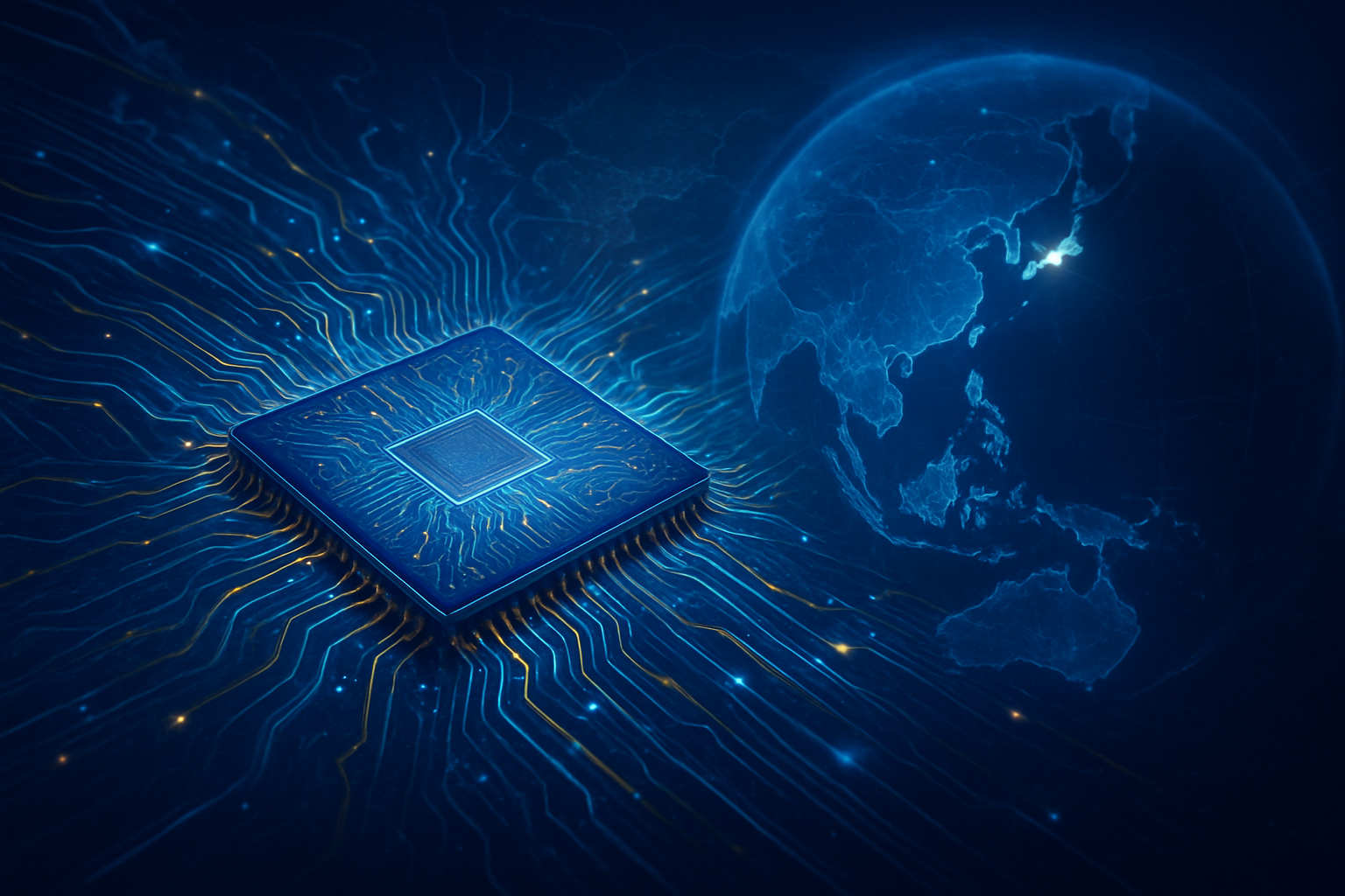
Tag: Semiconductors

  • Geopolitical Tides Force TSMC to Diversify: Reshaping the Global Chip Landscape

    Geopolitical Tides Force TSMC to Diversify: Reshaping the Global Chip Landscape

    Taipei, Taiwan – December 1, 2025 – The world's preeminent contract chipmaker, Taiwan Semiconductor Manufacturing Company (TSMC) (NYSE: TSM), is actively charting a course beyond its home shores, driven by an intricate web of geopolitical tensions and national security imperatives. This strategic pivot, characterized by monumental investments in new fabrication plants across the United States, Japan, and Europe, marks a significant reorientation for the global semiconductor industry, aiming to de-risk supply chains and foster greater regional technological sovereignty. As political shifts intensify, TSMC's diversification efforts are not merely an expansion but a fundamental reshaping of where and how the world's most critical components are manufactured, with profound implications for everything from smartphones to advanced AI systems.

    This proactive decentralization strategy, while costly and complex, underscores a global recognition of the vulnerabilities inherent in a highly concentrated semiconductor supply chain. The move is a direct response to escalating concerns over potential disruptions in the Taiwan Strait, alongside a concerted push from major economies to bolster domestic chip production capabilities. For the global tech industry, TSMC's outward migration signals a new era of localized manufacturing, promising enhanced resilience but also introducing new challenges related to cost, talent, and the intricate ecosystem that has long flourished in Taiwan.

    A Global Network of Advanced Fabs Emerges Amidst Geopolitical Crosscurrents

    TSMC's ambitious global manufacturing expansion is rapidly taking shape across key strategic regions, each facility representing a crucial node in a newly diversified network. In the United States, the company has committed an unprecedented $165 billion to establish three production facilities, two advanced packaging plants, and a research and development center in Arizona. The first Arizona factory has already commenced production of 4-nanometer chips, with subsequent facilities slated for even more advanced 2-nanometer chips. Projections suggest that once fully operational, these six plants could account for approximately 30% of TSMC's most advanced chip production.

    Concurrently, TSMC has inaugurated its first plant in Kumamoto, Japan, through a joint venture, Japan Advanced Semiconductor Manufacturing (JASM), focusing on chips in the 12nm to 28nm range. This initiative, heavily supported by the Japanese government, is already slated for a second, more advanced plant capable of manufacturing 6nm-7nm chips, expected by the end of 2027. In Europe, TSMC broke ground on its first chip manufacturing plant in Dresden, Germany, in August 2024. This joint venture, European Semiconductor Manufacturing Company (ESMC), with partners Infineon (FWB: IFX), Bosch (NSE: BOSCHLTD), and NXP (NASDAQ: NXPI), represents an investment exceeding €10 billion, with substantial German state subsidies. The Dresden plant will initially focus on mature technology nodes (28/22nm and 16/12nm) vital for the automotive and industrial sectors, with production commencing by late 2027.

    This multi-pronged approach significantly differs from TSMC's historical model, which saw the vast majority of its cutting-edge production concentrated in Taiwan. While Taiwan is still expected to remain the central hub for TSMC's most advanced chip production, accounting for over 90% of its total capacity and 90% of global advanced-node capacity, the new overseas fabs represent a strategic hedge. Initial reactions from the AI research community and industry experts highlight a cautious optimism, recognizing the necessity of supply chain resilience while also acknowledging the immense challenges of replicating Taiwan's highly efficient, integrated semiconductor ecosystem in new locations. The cost implications and potential for slower ramp-ups are frequently cited concerns, yet the strategic imperative for diversification largely outweighs these immediate hurdles.

    Redrawing the Competitive Landscape for Tech Giants and Startups

    TSMC's global manufacturing pivot is poised to significantly impact AI companies, tech giants, and startups alike, redrawing the competitive landscape and influencing strategic advantages. Companies heavily reliant on TSMC's cutting-edge processors – including titans like Apple (NASDAQ: AAPL), NVIDIA (NASDAQ: NVDA), and AMD (NASDAQ: AMD) – stand to benefit from a more geographically diverse and resilient supply chain. The establishment of fabs in the US and Japan, for instance, offers these firms greater assurance against potential geopolitical disruptions in the Indo-Pacific, potentially reducing lead times and logistical complexities for chips destined for North American and Asian markets.

    This diversification also intensifies competition among major AI labs and tech companies. While TSMC's moves are aimed at de-risking for its customers, they also implicitly challenge other foundries like Samsung Foundry and Intel Foundry Services (NASDAQ: INTC) to accelerate their own global expansion and technological advancements. Intel, in particular, with its aggressive IDM 2.0 strategy, is vying to reclaim its leadership in process technology and foundry services, and TSMC's decentralized approach creates new arenas for this rivalry. The increased capacity for advanced nodes globally could also slightly ease supply constraints, potentially benefiting AI startups that require access to high-performance computing chips for their innovative solutions, though the cost of these chips may still remain a significant barrier.

    The potential disruption to existing products or services is minimal in the short term, as the new fabs will take years to reach full production. However, in the long term, a more resilient supply chain could lead to more stable product launches and potentially lower costs if efficiencies can be achieved in the new locations. Market positioning and strategic advantages will increasingly hinge on companies' ability to leverage these new manufacturing hubs. Tech giants with significant R&D presence near the new fabs might find opportunities for closer collaboration with TSMC, potentially accelerating custom chip development and integration. For countries like the US, Japan, and Germany, attracting these investments enhances their technological sovereignty and fosters a domestic ecosystem of suppliers and talent, further solidifying their strategic importance in the global tech sphere.

    A Crucial Step Towards Global Chip Supply Chain Resilience

    TSMC's strategic global expansion represents a crucial development in the broader AI and technology landscape, directly addressing the vulnerabilities exposed by an over-reliance on a single geographic region for advanced semiconductor manufacturing. This move fits squarely into the overarching trend of "de-risking" global supply chains, a phenomenon accelerated by the COVID-19 pandemic and exacerbated by heightened geopolitical tensions, particularly concerning Taiwan. The implications extend far beyond mere chip production, touching upon national security, economic stability, and the future trajectory of technological innovation.

    The primary impact is a tangible enhancement of global chip supply chain resilience. By establishing fabs in the US, Japan, and Germany, TSMC is creating redundancy and reducing the catastrophic potential of a single-point failure, whether due to natural disaster or geopolitical conflict. This is a direct response to the "silicon shield" debate, where Taiwan's critical role in advanced chip manufacturing was seen as a deterrent to invasion. While Taiwan will undoubtedly retain its leading edge in the most advanced nodes, the diversification ensures that a significant portion of crucial chip production is secured elsewhere. Potential concerns, however, include the higher operational costs associated with manufacturing outside Taiwan's highly optimized ecosystem, potential challenges in talent acquisition, and the sheer complexity of replicating an entire supply chain abroad.

    Comparisons to previous AI milestones and breakthroughs highlight the foundational nature of this development. Just as advancements in AI algorithms and computing power have been transformative, ensuring the stable and secure supply of the underlying hardware is equally critical. Without reliable access to advanced semiconductors, the progress of AI, high-performance computing, and other cutting-edge technologies would be severely hampered. This strategic shift by TSMC is not just about building factories; it's about fortifying the very infrastructure upon which the next generation of AI innovation will be built, safeguarding against future disruptions that could ripple across every tech-dependent industry globally.

    The Horizon: New Frontiers and Persistent Challenges

    Looking ahead, TSMC's global diversification is set to usher in a new era of semiconductor manufacturing, with expected near-term and long-term developments that will redefine the industry. In the near term, the focus will be on the successful ramp-up of the initial fabs in Arizona, Kumamoto, and Dresden. The commissioning of the 2-nanometer facilities in Arizona and the 6-7nm plant in Japan by the late 2020s will be critical milestones, significantly boosting the global capacity for these advanced nodes. The establishment of TSMC's first European design hub in Germany in Q3 2025 further signals a commitment to fostering local talent and innovation, paving the way for more integrated regional ecosystems.

    Potential applications and use cases on the horizon are vast. A more diversified and resilient chip supply chain will accelerate the development and deployment of next-generation AI, autonomous systems, advanced networking infrastructure (5G/6G), and sophisticated industrial automation. Countries hosting these fabs will likely see an influx of related industries and research, creating regional tech hubs that can innovate more rapidly with direct access to advanced manufacturing. For instance, the Dresden fab's focus on automotive chips will directly benefit Europe's robust auto industry, enabling faster integration of AI and advanced driver-assistance systems.

    However, significant challenges need to be addressed. The primary hurdle remains the higher cost of manufacturing outside Taiwan, which could impact TSMC's margins and potentially lead to higher chip prices. Talent acquisition and development in new regions are also critical, as Taiwan's highly skilled workforce and specialized ecosystem are difficult to replicate. Infrastructure development, including reliable power and water supplies, is another ongoing challenge. Experts predict that while Taiwan will maintain its lead in the absolute cutting edge, the trend of geographical diversification will continue, with more countries vying for domestic chip production capabilities. The coming years will reveal the true operational efficiencies and cost structures of these new global fabs, shaping future investment decisions and the long-term balance of power in the semiconductor world.

    A New Chapter for Global Semiconductor Resilience

    TSMC's strategic move to diversify its manufacturing footprint beyond Taiwan represents one of the most significant shifts in the history of the semiconductor industry. The key takeaway is a global imperative for resilience, driven by geopolitical realities and the lessons learned from recent supply chain disruptions. This monumental undertaking is not merely about building new factories; it's about fundamentally re-architecting the foundational infrastructure of the digital world, creating a more robust and geographically distributed network for advanced chip production.

    Assessing this development's significance in AI history, it is clear that while AI breakthroughs capture headlines, the underlying hardware infrastructure is equally critical. TSMC's diversification ensures the continued, stable supply of the advanced silicon necessary to power the next generation of AI innovations, from large language models to complex robotics. It mitigates the existential risk of a single point of failure, thereby safeguarding the relentless march of technological progress. The long-term impact will be a more secure, albeit potentially more expensive, global supply chain, fostering greater technological sovereignty for participating nations and a more balanced distribution of manufacturing capabilities.

    In the coming weeks and months, industry observers will be watching closely for updates on the construction and ramp-up of these new fabs, particularly the progress on advanced node production in Arizona and Japan. Further announcements regarding partnerships, talent recruitment, and government incentives in host countries will also provide crucial insights into the evolving landscape. The success of TSMC's global strategy will not only determine its own future trajectory but will also set a precedent for how critical technologies are produced and secured in an increasingly complex and interconnected world.


    This content is intended for informational purposes only and represents analysis of current AI developments.

    TokenRing AI delivers enterprise-grade solutions for multi-agent AI workflow orchestration, AI-powered development tools, and seamless remote collaboration platforms.
    For more information, visit https://www.tokenring.ai/.

  • Canada’s Chip Ambition: Billions Flow to IBM and Marvell, Forging a North American Semiconductor Powerhouse

    Canada’s Chip Ambition: Billions Flow to IBM and Marvell, Forging a North American Semiconductor Powerhouse

    In a strategic pivot to bolster its position in the global technology landscape, the Canadian government, alongside provincial counterparts, is channeling significant financial incentives and support towards major US chipmakers like IBM (NYSE: IBM) and Marvell Technology Inc. (NASDAQ: MRVL). These multi-million dollar investments, culminating in recent announcements in November and December 2025, signify a concerted effort to cultivate a robust domestic semiconductor ecosystem, enhance supply chain resilience, and drive advanced technological innovation within Canada. The initiatives are designed not only to attract foreign direct investment but also to foster high-skilled job creation and secure Canada's role in the increasingly critical semiconductor industry.

    This aggressive push comes at a crucial time when global geopolitical tensions and supply chain vulnerabilities have underscored the strategic importance of semiconductor manufacturing. By providing substantial grants, loans, and strategic funding through programs like the Strategic Innovation Fund and Invest Ontario, Canada is actively working to de-risk and localize key aspects of chip production. The immediate significance of these developments is profound, promising a surge in economic activity, the establishment of cutting-edge research and development hubs, and a strengthened North American semiconductor supply chain, crucial for industries ranging from AI and automotive to telecommunications and defense.

    Forging Future Chips: Advanced Packaging and AI-Driven R&D

    The detailed technical scope of these initiatives highlights Canada's focus on high-value segments of the semiconductor industry, particularly advanced packaging and next-generation AI-driven chip research. At the forefront is IBM Canada's Bromont facility and the MiQro Innovation Collaborative Centre (C2MI) in Quebec. In November 2025, the Government of Canada announced a federal investment of up to C$210 million towards a C$662 million project. This substantial funding aims to dramatically expand semiconductor packaging and commercialization capabilities, enabling IBM to develop and assemble more complex semiconductor packaging for advanced transistors. This includes intricate 3D stacking and heterogeneous integration techniques, critical for meeting the ever-increasing demands for improved device performance, power efficiency, and miniaturization in modern electronics. This builds on an earlier April 2024 joint investment of approximately C$187 million (federal and Quebec contributions) to strengthen assembly, testing, and packaging (ATP) capabilities. Quebec further bolstered this with a C$32-million forgivable loan for new equipment and a C$7-million loan to automate a packaging assembly line for telecommunications switches. IBM's R&D efforts will also focus on scalable manufacturing methods and advanced assembly processes to support diverse chip technologies.

    Concurrently, Marvell Technology Inc. is poised for a significant expansion in Ontario, supported by an Invest Ontario grant of up to C$17 million, announced in December 2025, for its planned C$238 million, five-year investment. Marvell's focus will be on driving research and development for next-generation AI semiconductor technologies. This expansion includes creating up to 350 high-quality jobs, establishing a new office near the University of Toronto, and scaling up existing R&D operations in Ottawa and York Region, including an 8,000-square-foot optical lab in Ottawa. This move underscores Marvell's commitment to advancing AI-specific hardware, which is crucial for accelerating machine learning workloads and enabling more powerful and efficient AI systems. These projects differ from previous approaches by moving beyond basic manufacturing or design, specifically targeting advanced packaging, which is increasingly becoming a bottleneck in chip performance, and dedicated AI hardware R&D, positioning Canada at the cutting edge of semiconductor innovation rather than merely as a recipient of mature technologies. Initial reactions from the AI research community and industry experts have been overwhelmingly positive, citing Canada's strategic foresight in identifying critical areas for investment and its potential to become a key player in specialized chip development.

    Beyond these direct investments, Canada's broader initiatives further underscore its commitment. The Strategic Innovation Fund (SIF) with its Semiconductor Challenge Callout (now C$250 million) and the Strategic Response Fund (SRF) are key mechanisms. In July 2024, C$120 million was committed via the SIF to CMC Microsystems for the Fabrication of Integrated Components for the Internet's Edge (FABrIC) network, a pan-Canadian initiative to accelerate semiconductor design, manufacturing, and commercialization. The Canadian Photonics Fabrication Centre (CPFC) also received C$90 million to upgrade its capacity as Canada's only pure-play compound semiconductor foundry. These diverse programs collectively aim to create a comprehensive ecosystem, supporting everything from fundamental research and design to advanced manufacturing and packaging.

    Shifting Tides: Competitive Implications and Strategic Advantages

    These significant investments are poised to create a ripple effect across the AI and tech industries, directly benefiting not only the involved companies but also shaping the competitive landscape. IBM (NYSE: IBM), a long-standing technology giant, stands to gain substantial strategic advantages. The enhanced capabilities at its Bromont facility, particularly in advanced packaging, will allow IBM to further innovate in its high-performance computing, quantum computing, and AI hardware divisions. This strengthens their ability to deliver cutting-edge solutions, potentially reducing reliance on external foundries for critical packaging steps and accelerating time-to-market for new products. The Canadian government's support also signals a strong partnership, potentially leading to further collaborations and a more robust supply chain for IBM's North American operations.

    Marvell Technology Inc. (NASDAQ: MRVL), a leader in data infrastructure semiconductors, will significantly bolster its R&D capabilities in AI. The C$238 million expansion, supported by Invest Ontario, will enable Marvell to accelerate the development of next-generation AI chips, crucial for its cloud, enterprise, and automotive segments. This investment positions Marvell to capture a larger share of the rapidly growing AI hardware market, enhancing its competitive edge against rivals in specialized AI accelerators and data center solutions. By establishing a new office near the University of Toronto and scaling operations in Ottawa and York Region, Marvell gains access to Canada's highly skilled talent pool, fostering innovation and potentially disrupting existing products by introducing more powerful and efficient AI-specific silicon. This strategic move strengthens Marvell's market positioning as a key enabler of AI infrastructure.

    Beyond these two giants, the initiatives are expected to foster a vibrant ecosystem for Canadian AI startups and smaller tech companies. Access to advanced packaging facilities through C2MI and the broader FABrIC network, along with the talent development spurred by these investments, could significantly lower barriers to entry for companies developing specialized AI hardware or integrated solutions. This could lead to new partnerships, joint ventures, and a more dynamic innovation environment. The competitive implications for major AI labs and tech companies globally are also notable; as Canada strengthens its domestic capabilities, it becomes a more attractive partner for R&D and potentially a source of critical components, diversifying the global supply chain and potentially offering alternatives to existing manufacturing hubs.

    A Geopolitical Chessboard: Broader Significance and Supply Chain Resilience

    Canada's aggressive pursuit of semiconductor independence and leadership fits squarely into the broader global AI landscape and current geopolitical trends. The COVID-19 pandemic starkly exposed the vulnerabilities of highly concentrated global supply chains, particularly in critical sectors like semiconductors. Nations worldwide, including the US, EU, Japan, and now Canada, are investing heavily in domestic chip production to enhance economic security and technological sovereignty. Canada's strategy, by focusing on specialized areas like advanced packaging and AI-specific R&D rather than attempting to replicate full-scale leading-edge fabrication, is a pragmatic approach to carving out a niche in a highly capital-intensive industry. This approach also aligns with North American efforts to build a more resilient and integrated supply chain, complementing initiatives in the United States and Mexico under the USMCA agreement.

    The impacts of these initiatives extend beyond economic metrics. They represent a significant step towards mitigating future supply chain disruptions that could cripple industries reliant on advanced chips, from electric vehicles and medical devices to telecommunications infrastructure and defense systems. By fostering domestic capabilities, Canada reduces its vulnerability to geopolitical tensions and trade disputes that could interrupt the flow of essential components. However, potential concerns include the immense capital expenditure required and the long lead times for return on investment. Critics might question the scale of government involvement or the potential for market distortions. Nevertheless, proponents argue that the strategic imperative outweighs these concerns, drawing comparisons to historical government-led industrial policies that catalyzed growth in other critical sectors. These investments are not just about chips; they are about securing Canada's economic future, enhancing national security, and ensuring its continued relevance in the global technological race. They represent a clear commitment to fostering a knowledge-based economy and positioning Canada as a reliable partner in the global technology ecosystem.

    The Road Ahead: Future Developments and Expert Predictions

    Looking ahead, these foundational investments are expected to catalyze a wave of near-term and long-term developments in Canada's semiconductor and AI sectors. In the immediate future, we can anticipate accelerated progress in advanced packaging techniques, with IBM's Bromont facility becoming a hub for innovative module integration and testing. This will likely lead to a faster commercialization of next-generation devices that demand higher performance and smaller footprints. Marvell's expanded R&D in AI chips will undoubtedly yield new silicon designs optimized for emerging AI workloads, potentially impacting everything from edge computing to massive data centers. We can also expect to see a surge in talent development, as these projects will create numerous co-op opportunities and specialized training programs, attracting and retaining top-tier engineers and researchers in Canada.

    Potential applications and use cases on the horizon are vast. The advancements in advanced packaging will enable more powerful and efficient processors for quantum computing initiatives, high-performance computing, and specialized AI accelerators. Improved domestic capabilities will also benefit Canada's burgeoning automotive technology sector, particularly in autonomous vehicles and electric vehicle power management, as well as its aerospace and defense industries, ensuring secure and reliable access to critical components. Furthermore, the focus on AI semiconductors will undoubtedly fuel innovations in areas like natural language processing, computer vision, and predictive analytics, leading to more sophisticated AI applications across various sectors.

    However, challenges remain. Attracting and retaining a sufficient number of highly skilled workers in a globally competitive talent market will be crucial. Sustaining long-term funding and political will beyond initial investments will also be essential to ensure the longevity and success of these initiatives. Furthermore, Canada will need to continuously adapt its strategy to keep pace with the rapid evolution of semiconductor technology and global market dynamics. Experts predict that Canada's strategic focus on niche, high-value segments like advanced packaging and AI-specific hardware will allow it to punch above its weight in the global semiconductor arena. They foresee Canada evolving into a key regional hub for specialized chip development and a critical partner in securing North American technological independence, especially as the demand for AI-specific hardware continues its exponential growth.

    Canada's Strategic Bet: A New Era for North American Semiconductors

    In summary, the Canadian government's substantial financial incentives and strategic support for US chipmakers like IBM and Marvell represent a pivotal moment in the nation's technological and economic history. These multi-million dollar investments, particularly the recent announcements in late 2025, are meticulously designed to foster a robust domestic semiconductor ecosystem, enhance advanced packaging capabilities, and accelerate research and development in next-generation AI chips. The immediate significance lies in the creation of high-skilled jobs, the attraction of significant foreign direct investment, and a critical boost to Canada's technological sovereignty and supply chain resilience.

    This development marks a significant milestone in Canada's journey to become a key player in the global semiconductor landscape. By strategically focusing on high-value segments and collaborating with industry leaders, Canada is not merely attracting manufacturing but actively participating in the innovation cycle of critical technologies. The long-term impact is expected to solidify Canada's position as an innovation hub, driving economic growth and securing its role in the future of AI and advanced computing. What to watch for in the coming weeks and months includes the definitive agreements for Marvell's expansion, the tangible progress at IBM's Bromont facility, and further announcements regarding the utilization of broader initiatives like the Semiconductor Challenge Callout. These developments will provide crucial insights into the execution and ultimate success of Canada's ambitious semiconductor strategy, signaling a new era for North American chip production.


    This content is intended for informational purposes only and represents analysis of current AI developments.

    TokenRing AI delivers enterprise-grade solutions for multi-agent AI workflow orchestration, AI-powered development tools, and seamless remote collaboration platforms.
    For more information, visit https://www.tokenring.ai/.

  • Marvell Technology Ignites Ontario’s AI Future with $238 Million Semiconductor Powerhouse

    Marvell Technology Ignites Ontario’s AI Future with $238 Million Semiconductor Powerhouse

    Ottawa, Ontario – December 1, 2025 – Marvell Technology Inc. (NASDAQ: MRVL) today announced a monumental five-year, $238 million investment into Ontario's burgeoning semiconductor research and development sector. This strategic financial injection is poised to dramatically accelerate the creation of next-generation semiconductor solutions, particularly those critical for the foundational infrastructure of artificial intelligence (AI) data centers. The move is expected to cement Ontario's status as a global leader in advanced technology and create up to 350 high-value technology jobs across the province.

    The substantial commitment from Marvell, a global leader in data infrastructure semiconductor solutions, underscores the escalating demand for specialized hardware to power the AI revolution. This investment, supported by an up to $17 million grant from the Ontario government's Invest Ontario Fund, is a clear signal of the province's growing appeal as a hub for cutting-edge technological innovation and a testament to its skilled workforce and robust tech ecosystem. It signifies a pivotal moment for regional tech development, promising to drive economic growth and intellectual capital in one of the world's most critical industries.

    Engineering Tomorrow's AI Infrastructure: A Deep Dive into Marvell's Strategic Expansion

    Marvell Technology Inc.'s $238 million investment is not merely a financial commitment but a comprehensive strategic expansion designed to significantly bolster its research and development capabilities in Canada. At the heart of this initiative is the expansion of semiconductor R&D operations in both Ottawa and the York Region, leveraging existing talent and infrastructure while pushing the boundaries of innovation. A key highlight of this expansion is the establishment of an 8,000-square-foot optical lab in Ottawa, a facility that will be instrumental in developing advanced optical technologies crucial for high-speed data transfer within AI data centers. Furthermore, Marvell plans to open a new office in Toronto, expanding its operational footprint and tapping into the city's diverse talent pool.

    This investment is meticulously targeted at advancing next-generation AI semiconductor technologies. Unlike previous generations of general-purpose chips, the demands of AI workloads necessitate highly specialized processors, memory, and interconnect solutions capable of handling massive datasets and complex parallel computations with unprecedented efficiency. Marvell's focus on AI data center infrastructure means developing chips that optimize power consumption, reduce latency, and enhance throughput—factors that are paramount for the performance and scalability of AI applications ranging from large language models to autonomous systems. The company's expertise in data infrastructure, already critical for major cloud-service providers like Amazon (NASDAQ: AMZN), Google (Alphabet Inc. – NASDAQ: GOOGL), and Microsoft (NASDAQ: MSFT), positions it uniquely to drive these advancements. This differs from previous approaches by directly addressing the escalating and unique hardware requirements of AI at an infrastructure level, rather than simply adapting existing architectures. Initial reactions from the AI research community and industry experts have been overwhelmingly positive, highlighting the critical need for such specialized hardware investments to keep pace with software innovations.

    The optical lab, in particular, represents a significant technical leap. Optical interconnects are becoming increasingly vital as electrical signals reach their physical limits in terms of speed and power efficiency over longer distances within data centers. By investing in this area, Marvell aims to develop solutions that will enable faster, more energy-efficient communication between processors, memory, and storage, which is fundamental for the performance of future AI supercomputers and distributed AI systems. This forward-looking approach ensures that Ontario will be at the forefront of developing the physical backbone for the AI era.

    Reshaping the AI Landscape: Competitive Implications and Market Dynamics

    Marvell Technology Inc.'s substantial investment in Ontario carries profound implications for AI companies, tech giants, and startups alike, promising to reshape competitive dynamics within the semiconductor and AI industries. Marvell (NASDAQ: MRVL) itself stands to significantly benefit by strengthening its leadership in data infrastructure semiconductor solutions, particularly in the rapidly expanding AI data center market. This strategic move will enable the company to accelerate its product roadmap, offer more advanced and efficient solutions to its clients, and capture a larger share of the market for AI-specific hardware.

    The competitive implications for major AI labs and tech companies are significant. Cloud giants such as Amazon (NASDAQ: AMZN), Google (Alphabet Inc. – NASDAQ: GOOGL), and Microsoft (NASDAQ: MSFT), which rely heavily on Marvell's technology for their data centers, stand to gain access to even more powerful and efficient semiconductor components. This could translate into faster AI model training, lower operational costs for their cloud AI services, and the ability to deploy more sophisticated AI applications. For other semiconductor players, this investment by Marvell intensifies the race for AI hardware dominance, potentially prompting rival companies to increase their own R&D spending and strategic partnerships to avoid being outpaced.

    This development could also lead to a potential disruption of existing products or services that rely on less optimized hardware. As Marvell pushes the boundaries of AI semiconductor efficiency and performance, companies that are slower to adopt these next-generation solutions might find their offerings becoming less competitive. Furthermore, the focus on specialized AI infrastructure provides Marvell with a strategic advantage, allowing it to deepen its relationships with key customers and potentially influence future industry standards for AI hardware. Startups in the AI space, particularly those developing innovative AI applications or specialized hardware, could find new opportunities for collaboration or access to cutting-edge components that were previously unavailable, fostering a new wave of innovation.

    Ontario's Ascent: Wider Significance in the Global AI Arena

    Marvell's $238 million investment is more than just a corporate expansion; it represents a significant milestone in the broader AI landscape and reinforces critical global trends. This initiative squarely positions Ontario as a pivotal player in the global semiconductor supply chain, a sector that has faced immense pressure and strategic importance in recent years. By anchoring advanced semiconductor R&D within the province, Marvell is helping to build a more resilient and innovative foundation for the technologies that underpin almost every aspect of modern life, especially AI.

    The investment squarely addresses the escalating global demand for specialized semiconductors that power AI systems. As AI models grow in complexity and data intensity, the need for purpose-built hardware capable of efficient processing, memory management, and high-speed data transfer becomes paramount. Ontario's strengthened capacity in this domain will deepen its contribution to the foundational technologies of future AI innovations, from autonomous vehicles and smart cities to advanced medical diagnostics and scientific discovery. This move also aligns with a broader trend of governments worldwide recognizing the strategic importance of domestic semiconductor capabilities for national security and economic competitiveness.

    Potential concerns, though minimal given the positive nature of the investment, might revolve around ensuring a continuous supply of highly specialized talent to fill the 350 new jobs and future growth. However, Ontario's robust educational institutions and existing tech ecosystem are well-positioned to meet this demand. Comparisons to previous AI milestones, such as the development of powerful GPUs for parallel processing, highlight that advancements in hardware are often as critical as breakthroughs in algorithms for driving the AI revolution forward. This investment is not just about incremental improvements; it's about laying the groundwork for the next generation of AI capabilities, ensuring that the physical infrastructure can keep pace with the exponential growth of AI software.

    The Road Ahead: Anticipating Future Developments and Applications

    The Marvell Technology Inc. investment into Ontario's semiconductor research signals a future brimming with accelerated innovation and transformative applications. In the near term, we can expect a rapid expansion of Marvell's R&D capabilities in Ottawa and York Region, with the new 8,000-square-foot optical lab in Ottawa becoming operational and driving breakthroughs in high-speed, energy-efficient data communication. The immediate impact will be the creation of up to 350 new, high-value technology jobs, attracting top-tier engineering and research talent to the province and further enriching Ontario's tech ecosystem.

    Looking further ahead, the long-term developments will likely see the emergence of highly specialized AI semiconductor solutions that are even more efficient, powerful, and tailored to specific AI workloads. These advancements will have profound implications across various sectors. Potential applications and use cases on the horizon include ultra-low-latency AI inference at the edge for real-time autonomous systems, significantly more powerful and energy-efficient AI training supercomputers, and revolutionary capabilities in areas like drug discovery, climate modeling, and personalized medicine, all powered by the underlying hardware innovations. The challenges that need to be addressed primarily involve continuous talent development, ensuring the infrastructure can support the growing demands of advanced manufacturing and research, and navigating the complexities of global supply chains.

    Experts predict that this investment will not only solidify Ontario's position as a global AI and semiconductor hub but also foster a virtuous cycle of innovation. As more advanced chips are developed, they will enable more sophisticated AI applications, which in turn will drive demand for even more powerful hardware. This continuous feedback loop is expected to accelerate the pace of AI development significantly. What happens next will be closely watched by the industry, as the initial breakthroughs from this enhanced R&D capacity begin to emerge, potentially setting new benchmarks for AI performance and efficiency.

    Forging the Future: A Comprehensive Wrap-up of a Landmark Investment

    Marvell Technology Inc.'s $238 million investment in Ontario's semiconductor research marks a pivotal moment for both the company and the province, solidifying a strategic alliance aimed at propelling the future of artificial intelligence. The key takeaways from this landmark announcement include the substantial financial commitment, the creation of up to 350 high-value jobs, and the strategic focus on next-generation AI data center infrastructure and optical technologies. This move not only reinforces Marvell's (NASDAQ: MRVL) leadership in data infrastructure semiconductors but also elevates Ontario's standing as a critical global hub for advanced technology and AI innovation.

    This development's significance in AI history cannot be overstated. It underscores the fundamental truth that software breakthroughs are intrinsically linked to hardware capabilities. By investing heavily in the foundational semiconductor technologies required for advanced AI, Marvell is directly contributing to the acceleration of AI's potential, enabling more complex models, faster processing, and more widespread applications. It represents a crucial step in building the robust, efficient, and scalable infrastructure that the burgeoning AI industry desperately needs.

    The long-term impact of this investment is expected to be transformative, fostering sustained economic growth, attracting further foreign direct investment, and cultivating a highly skilled workforce in Ontario. It positions the province at the forefront of a technology revolution that will redefine industries and societies globally. In the coming weeks and months, industry observers will be watching for the initial phases of this expansion, the hiring of new talent, and early indications of the research directions being pursued within the new optical lab and expanded R&D facilities. This investment is a powerful testament to the collaborative efforts between industry and government to drive innovation and secure a competitive edge in the global tech landscape.


    This content is intended for informational purposes only and represents analysis of current AI developments.

    TokenRing AI delivers enterprise-grade solutions for multi-agent AI workflow orchestration, AI-powered development tools, and seamless remote collaboration platforms.
    For more information, visit https://www.tokenring.ai/.

  • Alpha and Omega Semiconductor to Illuminate Future of Power at 14th Annual NYC Summit 2025

    Alpha and Omega Semiconductor to Illuminate Future of Power at 14th Annual NYC Summit 2025

    As the semiconductor industry continues its rapid evolution, driven by the insatiable demands of artificial intelligence and advanced computing, industry gatherings like the 14th Annual NYC Summit 2025 serve as critical junctures for innovation, investment, and strategic alignment. Alpha and Omega Semiconductor Limited (NASDAQ: AOSL), a leading designer and developer of power semiconductors, is set to participate in this exclusive investor conference on December 16, 2025, underscoring the vital role such events play in shaping the future of the tech landscape. Their presence highlights the growing importance of power management solutions in enabling next-generation technologies, particularly in the burgeoning AI sector.

    The NYC Summit, an invitation-only event tailored for accredited investors and publishing research analysts, offers a unique platform for companies like AOSL to engage directly with key financial stakeholders. Hosted collectively by participating companies, the summit facilitates in-depth discussions through a "round-robin" format, allowing for detailed exploration of business operations, strategic initiatives, and future outlooks. For Alpha and Omega Semiconductor, this represents a prime opportunity to showcase its advancements in power MOSFETs, wide bandgap devices (SiC and GaN), and power management ICs, which are increasingly crucial for the efficient and reliable operation of AI servers, data centers, and electric vehicles.

    Powering the AI Revolution: AOSL's Technical Edge

    Alpha and Omega Semiconductor (NASDAQ: AOSL) has positioned itself at the forefront of the power semiconductor market, offering a comprehensive portfolio designed to meet the rigorous demands of modern electronics. Their product lineup includes a diverse array of discrete power devices, such as low, medium, and high voltage Power MOSFETs, IGBTs, and IPMs, alongside advanced power management integrated circuits. A significant differentiator for AOSL is its integrated approach, combining proprietary semiconductor process technology, product design, and advanced packaging expertise to deliver high-performance solutions that push the boundaries of efficiency and power density.

    AOSL's recent announcement in October 2025 regarding its support for 800 VDC power architecture for next-generation AI factories exemplifies its commitment to innovation. This initiative leverages their cutting-edge SiC, GaN, Power MOSFET, and Power IC solutions to address the escalating power requirements of AI computing infrastructure. This differs significantly from traditional 48V or 12V architectures, enabling greater energy efficiency, reduced power loss, and enhanced system reliability crucial for the massive scale of AI data centers. Initial reactions from the AI research community and industry experts have emphasized the necessity of such robust power delivery systems to sustain the exponential growth in AI computational demands, positioning AOSL as a key enabler for future AI advancements.

    Competitive Dynamics and Market Positioning

    Alpha and Omega Semiconductor's participation in the NYC Summit, coupled with its strategic focus on high-growth markets, carries significant competitive implications. Companies like AOSL, which specialize in critical power management components, stand to benefit immensely from the continued expansion of AI, automotive electrification, and high-performance computing. Their diversified market focus, extending beyond traditional computing to consumer, industrial, and especially automotive sectors, provides resilience and multiple avenues for growth. The move to support 800 VDC for AI factories not only strengthens their position in the data center market but also demonstrates foresight in addressing future power challenges.

    The competitive landscape in power semiconductors is intense, with major players vying for market share. However, AOSL's integrated manufacturing capabilities and continuous innovation in wide bandgap materials (SiC and GaN) offer a strategic advantage. These materials are superior to traditional silicon in high-power, high-frequency applications, making them indispensable for electric vehicles and AI infrastructure. By showcasing these capabilities at investor summits, AOSL can attract crucial investment, foster partnerships, and reinforce its market positioning against larger competitors. Potential disruption to existing products or services could arise from competitors failing to adapt to the higher power density and efficiency demands of emerging technologies, leaving a significant opportunity for agile innovators like AOSL.

    Broader Significance in the AI Landscape

    AOSL's advancements and participation in events like the NYC Summit underscore a broader trend within the AI landscape: the increasing importance of foundational hardware. While much attention often focuses on AI algorithms and software, the underlying power infrastructure is paramount. Efficient power management is not merely an engineering detail; it is a bottleneck and an enabler for the next generation of AI. As AI models become larger and more complex, requiring immense computational power, the ability to deliver clean, stable, and highly efficient power becomes critical. AOSL's support for 800 VDC architecture directly addresses this, fitting into the broader trend of optimizing every layer of the AI stack for performance and sustainability.

    This development resonates with previous AI milestones, where hardware advancements, such as specialized GPUs, were crucial for breakthroughs. Today, power semiconductors are experiencing a similar moment of heightened importance. Potential concerns revolve around supply chain resilience and the pace of adoption of new power architectures. However, the energy efficiency gains offered by these solutions are too significant to ignore, especially given global efforts to reduce carbon footprints. The focus on high-voltage systems and wide bandgap materials marks a significant pivot, comparable to the shift from CPUs to GPUs for deep learning, signaling a new era of power optimization for AI.

    The Road Ahead: Future Developments and Challenges

    Looking ahead, the semiconductor industry, particularly in power management for AI, is poised for significant near-term and long-term developments. Experts predict continued innovation in wide bandgap materials, with SiC and GaN technologies becoming increasingly mainstream across automotive, industrial, and data center applications. AOSL's commitment to these areas positions it well for future growth. Expected applications include more compact and efficient power supplies for edge AI devices, advanced charging infrastructure for EVs, and even more sophisticated power delivery networks within future AI supercomputers.

    However, challenges remain. The cost of manufacturing SiC and GaN devices, though decreasing, still presents a barrier to widespread adoption in some segments. Furthermore, the complexity of designing and integrating these advanced power solutions requires specialized expertise. What experts predict is a continued push towards higher levels of integration, with more functions being consolidated into single power management ICs or modules, simplifying design for end-users. There will also be a strong emphasis on reliability and thermal management as power densities increase. AOSL's integrated approach and focus on advanced packaging will be crucial in addressing these challenges and capitalizing on emerging opportunities.

    A Pivotal Moment for Power Semiconductors

    Alpha and Omega Semiconductor's participation in the 14th Annual NYC Summit 2025 is more than just a corporate appearance; it is a testament to the pivotal role power semiconductors play in the unfolding AI revolution. The summit provides a crucial forum for AOSL to articulate its vision and demonstrate its technical prowess to the investment community, ensuring that the financial world understands the foundational importance of efficient power management. Their innovations, particularly in supporting 800 VDC for AI factories, underscore a significant shift in how AI infrastructure is powered, promising greater efficiency and performance.

    As we move into 2026 and beyond, the long-term impact of these developments will be profound. The ability to efficiently power increasingly complex AI systems will dictate the pace of innovation across numerous industries. What to watch for in the coming weeks and months includes further announcements on wide bandgap product expansions, strategic partnerships aimed at broader market penetration, and the continued integration of power management solutions into next-generation AI platforms. AOSL's journey exemplifies the critical, often unsung, role of hardware innovation in driving the future of artificial intelligence.


    This content is intended for informational purposes only and represents analysis of current AI developments.

    TokenRing AI delivers enterprise-grade solutions for multi-agent AI workflow orchestration, AI-powered development tools, and seamless remote collaboration platforms.
    For more information, visit https://www.tokenring.ai/.

  • Sealsq (NASDAQ: LAES) Soars on Strategic AI Leadership Appointment, Signaling Market Confidence in Dedicated AI Vision

    Sealsq (NASDAQ: LAES) Soars on Strategic AI Leadership Appointment, Signaling Market Confidence in Dedicated AI Vision

    Geneva, Switzerland – December 1, 2025 – SEALSQ Corp (NASDAQ: LAES), a company at the forefront of semiconductors, PKI, and post-quantum technologies, has captured significant market attention following the strategic appointment of Dr. Ballester Lafuente as its Chief of Staff and Group AI Officer. The announcement, made on November 24, 2025, has been met with a strong positive market reaction, with the company's stock experiencing a notable surge, reflecting investor confidence in SEALSQ's dedicated push into artificial intelligence. This executive move underscores a growing trend in the tech industry where specialized AI leadership is seen as a critical catalyst for innovation and market differentiation, particularly for companies navigating the complex interplay of advanced technologies.

    The appointment of Dr. Lafuente is a clear signal of SEALSQ's intensified commitment to integrating AI across its extensive portfolio. With his official start on November 17, 2025, Dr. Lafuente is tasked with orchestrating the company's AI strategy, aiming to embed intelligent capabilities into semiconductors, Public Key Infrastructure (PKI), Internet of Things (IoT), satellite technology, and the burgeoning field of post-quantum technologies. This comprehensive approach is designed not just to enhance individual product lines but to fundamentally transform SEALSQ's operational efficiency, accelerate innovation cycles, and carve out a distinct competitive edge in the rapidly evolving global tech landscape. The market's enthusiastic response highlights the increasing value placed on robust, dedicated AI leadership in driving corporate strategy and unlocking future growth.

    The Architect of AI Integration: Dr. Lafuente's Vision for SEALSQ

    Dr. Ballester Lafuente brings a formidable background to his new dual role, positioning him as a pivotal figure in SEALSQ's strategic evolution. His extensive expertise spans AI, digital innovation, and cybersecurity, cultivated through a diverse career that includes serving as Head of IT Innovation at the International Institute for Management Development (IMD) in Lausanne, and as a Technical Program Manager at the EPFL Center for Digital Trust (C4DT). Dr. Lafuente's academic credentials are equally impressive, holding a PhD in Management Information Systems from the University of Geneva and an MSc in Security and Mobile Computing, underscoring his deep theoretical and practical understanding of complex technological ecosystems.

    His mandate at SEALSQ is far-reaching: to lead the holistic integration of AI across all facets of the company. This involves driving operational efficiency, enabling smarter processes, and accelerating innovation to achieve sustainable growth and market differentiation. Unlike previous approaches where AI might have been siloed within specific projects, Dr. Lafuente's appointment signifies a strategic shift towards viewing AI as a foundational engine for overall company performance. This vision is deeply intertwined with SEALSQ's existing initiatives, such as the "Convergence" initiative, launched in August 2025, which aims to unify AI with Post-Quantum Cryptography, Tokenization, and Satellite Connectivity into a cohesive framework for digital trust.

    Furthermore, Dr. Lafuente will play a crucial role in the SEALQUANTUM Initiative, a significant investment of up to $20 million earmarked for cutting-edge startups specializing in quantum computing, Quantum-as-a-Service (QaaS), and AI-driven semiconductor technologies. This initiative aims to foster innovations in AI-powered chipsets that seamlessly integrate with SEALSQ's post-quantum semiconductors, promising enhanced processing efficiency and security. His leadership is expected to be instrumental in advancing the company's Quantum-Resistant AI Security efforts at the SEALQuantum.com Lab, which is backed by a $30 million investment capacity and focuses on developing cryptographic technologies to protect AI models and data from future cyber threats, including those posed by quantum computers.

    Reshaping the AI Landscape: Competitive Implications and Market Positioning

    The appointment of a dedicated Group AI Officer by SEALSQ (NASDAQ: LAES) signals a strategic maneuver with significant implications for the broader AI industry, impacting established tech giants and emerging startups alike. By placing AI at the core of its executive leadership, SEALSQ aims to accelerate its competitive edge in critical sectors such as secure semiconductors, IoT, and post-quantum cryptography. This move positions SEALSQ to potentially challenge larger players who may have a more fragmented or less centralized approach to AI integration across their diverse product lines.

    Companies like SEALSQ, with their focused investment in AI leadership, stand to benefit from streamlined decision-making, faster innovation cycles, and a more coherent AI strategy. This could lead to the development of highly differentiated products and services, particularly in the niche but critical areas of secure hardware and quantum-resistant AI. For tech giants, such appointments by smaller, agile competitors serve as a reminder of the need for continuous innovation and strategic alignment in AI. While major AI labs and tech companies possess vast resources, a dedicated, cross-functional AI leader can provide the agility and strategic clarity that sometimes gets diluted in larger organizational structures.

    The potential disruption extends to existing products and services that rely on less advanced or less securely integrated AI. As SEALSQ pushes for AI-powered chipsets and quantum-resistant AI security, it could set new industry standards for trust and performance. This creates competitive pressure for others to enhance their AI security protocols and integrate AI more deeply into their core offerings. Market positioning and strategic advantages will increasingly hinge on not just having AI capabilities, but on having a clear, unified vision for how AI enhances security, efficiency, and innovation across an entire product ecosystem, a vision that Dr. Lafuente is now tasked with implementing.

    Broader Significance: AI Leadership in the Evolving Tech Paradigm

    SEALSQ's move to appoint a Group AI Officer fits squarely within the broader AI landscape and trends emphasizing the critical role of executive leadership in navigating complex technological shifts. In an era where AI is no longer a peripheral technology but a central pillar of innovation, companies are increasingly recognizing that successful AI integration requires dedicated, high-level strategic oversight. This trend reflects a maturation of the AI industry, moving beyond purely technical development to encompass strategic implementation, ethical considerations, and market positioning.

    The impacts of such appointments are multifaceted. They signal to investors, partners, and customers a company's serious commitment to AI, often translating into increased market confidence and, as seen with SEALSQ, a positive stock reaction. This dedication to AI leadership also helps to attract top-tier talent, as experts seek environments where their work is strategically valued and integrated. However, potential concerns can arise if the appointed leader lacks the necessary cross-functional influence or if the organizational culture is resistant to radical AI integration. The success of such a role heavily relies on the executive's ability to bridge technical expertise with business strategy.

    Comparisons to previous AI milestones reveal a clear progression. Early AI breakthroughs focused on algorithmic advancements; more recently, the focus shifted to large language models and generative AI. Now, the emphasis is increasingly on how these powerful AI tools are strategically deployed and governed within an enterprise. SEALSQ's appointment signifies that dedicated AI leadership is becoming as crucial as a CTO or CIO in guiding a company through the complexities of the digital age, underscoring that the strategic application of AI is now a key differentiator and a driver of long-term value.

    The Road Ahead: Anticipated Developments and Future Challenges

    The appointment of Dr. Ballester Lafuente heralds a new era for SEALSQ (NASDAQ: LAES), with several near-term and long-term developments anticipated. In the near term, we can expect a clearer articulation of SEALSQ's AI roadmap under Dr. Lafuente's leadership, focusing on tangible integrations within its semiconductor and PKI offerings. This will likely involve pilot programs and early product enhancements showcasing AI-driven efficiencies and security improvements. The company's "Convergence" initiative, unifying AI with post-quantum cryptography and satellite connectivity, is also expected to accelerate, leading to integrated solutions for digital trust that could set new industry benchmarks.

    Looking further ahead, the potential applications and use cases are vast. SEALSQ's investment in AI-powered chipsets through its SEALQUANTUM Initiative could lead to a new generation of secure, intelligent hardware, impacting sectors from IoT devices to critical infrastructure. We might see AI-enhanced security features becoming standard in their semiconductors, offering proactive threat detection and quantum-resistant protection for sensitive data. Experts predict that the combination of AI and post-quantum cryptography, under dedicated leadership, could create highly resilient digital trust ecosystems, addressing the escalating cyber threats of both today and the quantum computing era.

    However, significant challenges remain. Integrating AI across diverse product lines and legacy systems is complex, requiring substantial investment in R&D, talent acquisition, and infrastructure. Ensuring the ethical deployment of AI, maintaining data privacy, and navigating evolving regulatory landscapes will also be critical. Furthermore, the high volatility of SEALSQ's stock, despite its strategic moves, indicates that market confidence is contingent on consistent execution and tangible results. What experts predict will happen next is a period of intense development and strategic partnerships, as SEALSQ aims to translate its ambitious AI vision into market-leading products and sustained financial performance.

    A New Chapter in AI Strategy: The Enduring Impact of Dedicated Leadership

    The appointment of Dr. Ballester Lafuente as SEALSQ's (NASDAQ: LAES) Group AI Officer marks a significant inflection point, not just for the company, but for the broader discourse on AI leadership in the tech industry. The immediate market enthusiasm, reflected in the stock's positive reaction, underscores a clear takeaway: investors are increasingly valuing companies that demonstrate a clear, dedicated, and executive-level commitment to AI integration. This move transcends a mere hiring; it's a strategic declaration that AI is fundamental to SEALSQ's future and will be woven into the very fabric of its operations and product development.

    This development's significance in AI history lies in its reinforcement of a growing trend: the shift from viewing AI as a specialized technical function to recognizing it as a core strategic imperative that requires C-suite leadership. It highlights that the successful harnessing of AI's transformative power demands not just technical expertise, but also strategic vision, cross-functional collaboration, and a holistic approach to implementation. As AI continues to evolve at an unprecedented pace, companies that embed AI leadership at the highest levels will likely be best positioned to innovate, adapt, and maintain a competitive edge.

    In the coming weeks and months, the tech world will be watching SEALSQ closely. Key indicators to watch include further details on Dr. Lafuente's specific strategic initiatives, announcements of new AI-enhanced products or partnerships, and the company's financial performance as these strategies begin to yield results. The success of this appointment will serve as a powerful case study for how dedicated AI leadership can translate into tangible business value and market leadership in an increasingly AI-driven global economy.


    This content is intended for informational purposes only and represents analysis of current AI developments.

    TokenRing AI delivers enterprise-grade solutions for multi-agent AI workflow orchestration, AI-powered development tools, and seamless remote collaboration platforms.
    For more information, visit https://www.tokenring.ai/.

  • The Symbiotic Revolution: How Software-Hardware Co-Design Unlocks the Next Generation of AI Chips

    The Symbiotic Revolution: How Software-Hardware Co-Design Unlocks the Next Generation of AI Chips

    The relentless march of artificial intelligence, particularly the exponential growth of large language models (LLMs) and generative AI, is pushing the boundaries of traditional computing. As AI models become more complex and data-hungry, the industry is witnessing a profound paradigm shift: the era of software and hardware co-design. This integrated approach, where the development of silicon and the algorithms it runs are inextricably linked, is no longer a luxury but a critical necessity for achieving optimal performance, energy efficiency, and scalability in the next generation of AI chips.

    Moving beyond the traditional independent development of hardware and software, co-design fosters a synergy that is immediately significant for overcoming the escalating demands of complex AI workloads. By tailoring hardware to specific AI algorithms and optimizing software to leverage unique hardware capabilities, systems can execute AI tasks significantly faster, reduce latency, and minimize power consumption. This collaborative methodology is driving innovation across the tech landscape, from hyperscale data centers to the burgeoning field of edge AI, promising to unlock unprecedented capabilities and reshape the future of intelligent computing.

    Technical Deep Dive: The Art of AI Chip Co-Design

    The shift to AI chip co-design marks a departure from the traditional "hardware-first" approach, where general-purpose processors were expected to run diverse software. Instead, co-design adopts a "software-first" or "top-down" philosophy, where the specific computational patterns and requirements of AI algorithms directly inform the design of specialized hardware. This tightly coupled development ensures that hardware features directly support software needs, and software is meticulously optimized to exploit the unique capabilities of the underlying silicon. This synergy is essential as Moore's Law struggles to keep pace with AI's insatiable appetite for compute, with AI compute needs doubling approximately every 3.5 months since 2012.

    Google's Tensor Processing Units (TPUs) exemplify this philosophy. These Application-Specific Integrated Circuits (ASICs) are purpose-built for AI workloads. At their heart lies the Matrix Multiply Unit (MXU), a systolic array designed for high-volume, low-precision matrix multiplications, a cornerstone of deep learning. TPUs also incorporate High Bandwidth Memory (HBM) and custom, high-speed interconnects like the Inter-Chip Interconnect (ICI), enabling massive clusters (up to 9,216 chips in a pod) to function as a single supercomputer. The software stack, including frameworks like TensorFlow, JAX, and PyTorch, along with the XLA (Accelerated Linear Algebra) compiler, is deeply integrated, translating high-level code into optimized instructions that leverage the TPU's specific hardware features. Google's latest Ironwood (TPU v7) is purpose-built for inference, offering nearly 30x more power efficiency than earlier versions and reaching 4,614 TFLOP/s of peak computational performance.

    NVIDIA's (NASDAQ: NVDA) Graphics Processing Units (GPUs), while initially designed for graphics, have evolved into powerful AI accelerators through significant architectural and software innovations rooted in co-design. Beyond their general-purpose CUDA Cores, NVIDIA introduced specialized Tensor Cores with the Volta architecture in 2017. These cores are explicitly designed to accelerate matrix multiplication operations crucial for deep learning, supporting mixed-precision computing (e.g., FP8, FP16, BF16). The Hopper architecture (H100) features fourth-generation Tensor Cores with FP8 support via the Transformer Engine, delivering up to 3,958 TFLOPS for FP8. NVIDIA's CUDA platform, along with libraries like cuDNN and TensorRT, forms a comprehensive software ecosystem co-designed to fully exploit Tensor Cores and other architectural features, integrating seamlessly with popular frameworks. The H200 Tensor Core GPU, built on Hopper, features 141GB of HBM3e memory with 4.8TB/s bandwidth, nearly doubling the H100's capacity and bandwidth.

    Beyond these titans, a wave of emerging custom ASICs from various companies and startups further underscores the co-design principle. These accelerators are purpose-built for specific AI workloads, often featuring optimized memory access, larger on-chip caches, and support for lower-precision arithmetic. Companies like Tesla (NASDAQ: TSLA) with its Full Self-Driving (FSD) Chip, and others developing Neural Processing Units (NPUs), demonstrate a growing trend towards specialized silicon for real-time inference and specific AI tasks. The AI research community and industry experts universally view hardware-software co-design as not merely beneficial but critical for the future of AI, recognizing its necessity for efficient, scalable, and energy-conscious AI systems. There's a growing consensus that AI itself is increasingly being leveraged in the chip design process, with AI agents automating and optimizing various stages of chip design, from logic synthesis to floorplanning, leading to what some call "unintuitive" designs that outperform human-engineered counterparts.

    Reshaping the AI Industry: Competitive Implications

    The profound shift towards AI chip co-design is dramatically reshaping the competitive landscape for AI companies, tech giants, and startups alike. Vertical integration, where companies control their entire technology stack from hardware to software, is emerging as a critical strategic advantage.

    Tech giants are at the forefront of this revolution. Google (NASDAQ: GOOGL), with its TPUs, benefits from massive performance-per-dollar advantages and reduced reliance on external GPU suppliers. This deep control over both hardware and software, with direct feedback loops between chip designers and AI teams like DeepMind, provides a significant moat. NVIDIA, while still dominant in the AI hardware market, is actively forming strategic partnerships with companies like Intel (NASDAQ: INTC) and Synopsys (NASDAQ: SNPS) to co-develop custom data center and PC products and boost AI in chip design. NVIDIA is also reportedly building a unit to design custom AI chips for cloud customers, acknowledging the growing demand for specialized solutions. Microsoft (NASDAQ: MSFT) has introduced its own custom silicon, Azure Maia for AI acceleration and Azure Cobalt for general-purpose cloud computing, aiming to optimize performance, security, and power consumption for its Azure cloud and AI workloads. This move, which includes incorporating OpenAI's custom chip designs, aims to reduce reliance on third-party suppliers and boost competitiveness. Similarly, Amazon Web Services (NASDAQ: AMZN) has invested heavily in custom Inferentia chips for AI inference and Trainium chips for AI model training, securing its position in cloud computing and offering superior power efficiency and cost-effectiveness.

    This trend intensifies competition, particularly challenging NVIDIA's dominance. While NVIDIA's CUDA ecosystem remains powerful, the proliferation of custom chips from hyperscalers offers superior performance-per-dollar for specific workloads, forcing NVIDIA to innovate and adapt. The competition extends beyond hardware to the software ecosystems that support these chips, with tech giants building robust software layers around their custom silicon.

    For startups, AI chip co-design presents both opportunities and challenges. AI-powered Electronic Design Automation (EDA) tools are lowering barriers to entry, potentially reducing design time from months to weeks and enabling smaller players to innovate faster and more cost-effectively. Startups focusing on niche AI applications or specific hardware-software optimizations can carve out unique market positions. However, the immense cost and complexity of developing cutting-edge AI semiconductors remain a significant hurdle, though specialized AI design tools and partnerships can help mitigate these. This disruption also extends to existing products and services, as general-purpose hardware becomes increasingly inefficient for highly specialized AI tasks, leading to a shift towards custom accelerators and a rethinking of AI infrastructure. Companies with vertical integration gain strategic independence, cost control, supply chain resilience, and the ability to accelerate innovation, providing a proprietary advantage in the rapidly evolving AI landscape.

    Wider Significance: Beyond the Silicon

    The widespread adoption of software and hardware co-design in AI chips represents a fundamental shift in how AI systems are conceived and built, carrying profound implications for the broader AI landscape, energy consumption, and accessibility.

    This integrated approach is indispensable given current AI trends, including the growing complexity of AI models like LLMs, the demand for real-time AI in applications such as autonomous vehicles, and the proliferation of Edge AI in resource-constrained devices. Co-design allows for the creation of specialized accelerators and optimized memory hierarchies that can handle massive workloads more efficiently, delivering ultra-low latency, and enabling AI inference on compact, energy-efficient devices. Crucially, AI itself is increasingly being leveraged as a co-design tool, with AI-powered tools assisting in architecture exploration, RTL design, synthesis, and verification, creating an "innovation flywheel" that accelerates chip development.

    The impacts are profound: drastic performance improvements, enabling faster execution and higher throughput; significant reductions in energy consumption, vital for large-scale AI deployments and sustainable AI; and the enabling of entirely new capabilities in fields like autonomous driving and personalized medicine. While the initial development costs can be high, long-term operational savings through improved efficiency can be substantial.

    However, potential concerns exist. The increased complexity and development costs could lead to market concentration, with large tech companies dominating advanced AI hardware, potentially limiting accessibility for smaller players. There's also a trade-off between specialization and generality; highly specialized co-designs might lack the flexibility to adapt to rapidly evolving AI models. The industry also faces a talent gap in engineers proficient in both hardware and software aspects of AI.

    Comparing this to previous AI milestones, co-design represents an evolution beyond the GPU era. While GPUs marked a breakthrough for deep learning, they were general-purpose accelerators. Co-design moves towards purpose-built or finely-tuned hardware-software stacks, offering greater specialization and efficiency. As Moore's Law slows, co-design offers a new path to continued performance gains by optimizing the entire system, demonstrating that innovation can come from rethinking the software stack in conjunction with hardware architecture.

    Regarding energy consumption, AI's growing footprint is a critical concern. Co-design is a key strategy for mitigation, creating highly efficient, specialized chips that dramatically reduce the power required for AI inference and training. Innovations like embedding memory directly into chips promise further energy efficiency gains. Accessibility is a double-edged sword: while high entry barriers could lead to market concentration, long-term efficiency gains could make AI more cost-effective and accessible through cloud services or specialized edge devices. AI-powered design tools, if widely adopted, could also democratize chip design. Ultimately, co-design will profoundly shape the future of AI development, driving the creation of increasingly specialized hardware for new AI paradigms and accelerating an innovation feedback loop.

    The Horizon: Future Developments in AI Chip Co-Design

    The future of AI chip co-design is dynamic and transformative, marked by continuous innovation in both design methodologies and underlying technologies. Near-term developments will focus on refining existing trends, while long-term visions paint a picture of increasingly autonomous and brain-inspired AI systems.

    In the near term, AI-driven chip design (AI4EDA) will become even more pervasive, with AI-powered Electronic Design Automation (EDA) tools automating circuit layouts, enhancing verification, and optimizing power, performance, and area (PPA). Generative AI will be used to explore vast design spaces, suggest code, and even generate full sub-blocks from functional specifications. We'll see a continued rise in specialized accelerators for specific AI workloads, particularly for transformer and diffusion models, with hyperscalers developing custom ASICs that outperform general-purpose GPUs in efficiency for niche tasks. Chiplet-based designs and heterogeneous integration will become the norm, allowing for flexible scaling and the integration of multiple specialized chips into a single package. Advanced packaging techniques like 2.5D and 3D integration, CoWoS, and hybrid bonding will be critical for higher performance, improved thermal management, and lower power consumption, especially for generative AI. Memory-on-Package (MOP) and Near-Memory Compute will address data transfer bottlenecks, while RISC-V AI Cores will gain traction for lightweight inference at the edge.

    Long-term developments envision an ultimate state where AI-designed chips are created with minimal human intervention, leading to "AI co-designing the hardware and software that powers AI itself." Self-optimizing manufacturing processes, driven by AI, will continuously refine semiconductor fabrication. Neuromorphic computing, inspired by the human brain, will aim for highly efficient, spike-based AI processing. Photonics and optical interconnects will reduce latency for next-gen AI chips, integrating electrical and photonic ICs. While nascent, quantum computing integration will also rely on co-design principles. The discovery and validation of new materials for smaller process nodes and advanced 3D architectures, such as indium-based materials for EUV patterning and new low-k dielectrics, will be accelerated by AI.

    These advancements will unlock a vast array of potential applications. Cloud data centers will see continued acceleration of LLM training and inference. Edge AI will enable real-time decision-making in autonomous vehicles, smart homes, and industrial IoT. High-Performance Computing (HPC) will power advanced scientific modeling. Generative AI will become more efficient, and healthcare will benefit from enhanced AI capabilities for diagnostics and personalized treatments. Defense applications will see improved energy efficiency and faster response times.

    However, several challenges remain. The inherent complexity and heterogeneity of AI systems, involving diverse hardware and software frameworks, demand sophisticated co-design. Scalability for exponentially growing AI models and high implementation costs pose significant hurdles. Time-consuming iterations in the co-design process and ensuring compatibility across different vendors are also critical. The reliance on vast amounts of clean data for AI design tools, the "black box" nature of some AI decisions, and a growing skill gap in engineers proficient in both hardware and AI are also pressing concerns. The rapid evolution of AI models creates a "synchronization issue" where hardware can quickly become suboptimal.

    Experts predict a future of convergence and heterogeneity, with optimized designs for specific AI workloads. Advanced packaging is seen as a cornerstone of semiconductor innovation, as important as chip design itself. The "AI co-designing everything" paradigm is expected to foster an innovation flywheel, with silicon hardware becoming almost as "codable" as software. This will lead to accelerated design cycles and reduced costs, with engineers transitioning from "tool experts" to "domain experts" as AI handles mundane design aspects. Open-source standardization initiatives like RISC-V are also expected to play a role in ensuring compatibility and performance, ushering in an era of AI-native tooling that fundamentally reshapes design and manufacturing processes.

    The Dawn of a New Era: A Comprehensive Wrap-up

    The interplay of software and hardware in the development of next-generation AI chips is not merely an optimization but a fundamental architectural shift, marking a new era in artificial intelligence. The necessity of co-design, driven by the insatiable computational demands of modern AI, has propelled the industry towards a symbiotic relationship between silicon and algorithms. This integrated approach, exemplified by Google's TPUs and NVIDIA's Tensor Cores, allows for unprecedented levels of performance, energy efficiency, and scalability, far surpassing the capabilities of general-purpose processors.

    The significance of this development in AI history cannot be overstated. It represents a crucial pivot in response to the slowing of Moore's Law, offering a new pathway for continued innovation and performance gains. By tailoring hardware precisely to software needs, companies can unlock capabilities previously deemed impossible, from real-time autonomous systems to the efficient training of trillion-parameter generative AI models. This vertical integration provides a significant competitive advantage for tech giants like Google, NVIDIA, Microsoft, and Amazon, enabling them to optimize their cloud and AI services, control costs, and secure their supply chains. While posing challenges for startups due to high development costs, AI-powered design tools are simultaneously lowering barriers to entry, fostering a dynamic and competitive ecosystem.

    Looking ahead, the long-term impact of co-design will be transformative. The rise of AI-driven chip design will create an "innovation flywheel," where AI designs better chips, which in turn accelerate AI development. Innovations in advanced packaging, new materials, and the exploration of neuromorphic and quantum computing architectures will further push the boundaries of what's possible. However, addressing challenges such as complexity, scalability, high implementation costs, and the talent gap will be crucial for widespread adoption and equitable access to these powerful technologies.

    In the coming weeks and months, watch for continued announcements from major tech companies regarding their custom silicon initiatives and strategic partnerships in the chip design space. Pay close attention to advancements in AI-powered EDA tools and the emergence of more specialized accelerators for specific AI workloads. The race for AI dominance will increasingly be fought at the intersection of hardware and software, with co-design being the ultimate arbiter of performance and efficiency. This integrated approach is not just optimizing AI; it's redefining it, laying the groundwork for a future where intelligent systems are more powerful, efficient, and ubiquitous than ever before.


    This content is intended for informational purposes only and represents analysis of current AI developments.

    TokenRing AI delivers enterprise-grade solutions for multi-agent AI workflow orchestration, AI-powered development tools, and seamless remote collaboration platforms.
    For more information, visit https://www.tokenring.ai/.

  • The New Silicon Frontier: Geopolitics Reshapes Global Chipmaking and Ignites the AI Race

    The New Silicon Frontier: Geopolitics Reshapes Global Chipmaking and Ignites the AI Race

    The global semiconductor industry, the foundational bedrock of modern technology, is undergoing an unprecedented and profound restructuring. Driven by escalating geopolitical tensions, particularly the intensifying rivalry between the United States and China, nations are aggressively pursuing self-sufficiency in chipmaking. This strategic pivot, exemplified by landmark legislation like the US CHIPS Act, is fundamentally altering global supply chains, reshaping economic competition, and becoming the central battleground in the race for artificial intelligence (AI) supremacy. The immediate significance of these developments for the tech industry and national security cannot be overstated, signaling a definitive shift from a globally integrated model to one characterized by regionalized ecosystems and strategic autonomy.

    A New Era of Techno-Nationalism: The US CHIPS Act and Global Initiatives

    The current geopolitical landscape is defined by intense competition for technological leadership, with semiconductors at its core. The COVID-19 pandemic laid bare the fragility of highly concentrated global supply chains, highlighting the risks associated with the geographical concentration of advanced chip production, predominantly in East Asia. This vulnerability, coupled with national security imperatives, has spurred governments worldwide to launch ambitious chipmaking initiatives.

    The US CHIPS and Science Act, signed into law by President Joe Biden on August 9, 2022, is a monumental example of this strategic shift. It authorizes approximately $280 billion in new funding for science and technology, with a substantial $52.7 billion specifically appropriated for semiconductor-related programs for fiscal years 2022-2027. This includes $39 billion for manufacturing incentives, offering direct federal financial assistance (grants, loans, loan guarantees) to incentivize companies to build, expand, or modernize domestic facilities for semiconductor fabrication, assembly, testing, and advanced packaging. A crucial 25% Advanced Manufacturing Investment Tax Credit further sweetens the deal for qualifying investments. Another $13 billion is allocated for semiconductor Research and Development (R&D) and workforce training, notably for establishing the National Semiconductor Technology Center (NSTC) – a public-private consortium aimed at fostering collaboration and developing the future workforce.

    The Act's primary goal is to significantly boost the domestic production of leading-edge logic chips (sub-10nm). U.S. Commerce Secretary Gina Raimondo has set an ambitious target for the U.S. to produce approximately 20% of the world's leading-edge logic chips by the end of the decade, a substantial increase from near zero today. Companies like Intel (NASDAQ: INTC), TSMC (NYSE: TSM), and Samsung (KRX: 005930) are investing heavily in new U.S. fabs with plans to produce 2nm and 3nm chips. For instance, TSMC's second Arizona plant is slated to produce 2nm chips by 2028, and Intel is advancing its 18A process for 2025.

    This legislation marks a significant departure from previous U.S. industrial policy, signaling the most robust return to government backing for key industries since World War II. Unlike past, often indirect, approaches, the CHIPS Act provides billions in direct grants, loans, and significant tax credits specifically for semiconductor manufacturing and R&D. It is explicitly motivated by geopolitical concerns, strengthening American supply chain resilience, and countering China's technological advancements. The inclusion of "guardrail" provisions, prohibiting funding recipients from expanding advanced semiconductor manufacturing in countries deemed national security threats like China for ten years, underscores this assertive, security-centric approach.

    Initial reactions from the AI research community and industry experts have been largely positive, viewing the Act as a vital catalyst for AI advancement by ensuring a stable supply of necessary chips. However, concerns have been raised regarding slow fund distribution, worker shortages, high operating costs for new U.S. fabs, and potential disconnects between manufacturing and innovation funding. The massive scale of investment also raises questions about long-term sustainability and the risk of creating industries dependent on sustained government support.

    Reshaping the AI Ecosystem: Winners, Losers, and Strategic Shifts

    The national chipmaking initiatives, particularly the US CHIPS Act, are fundamentally reshaping the competitive landscape for AI companies, tech giants, and startups, creating both immense opportunities and significant challenges.

    Direct Beneficiaries: Semiconductor manufacturers committing to building or expanding facilities in the U.S. are the primary recipients of CHIPS Act funding. Intel (NASDAQ: INTC) has received substantial direct funding, including $8.5 billion for new facilities in Arizona, New Mexico, Ohio, and Oregon, bolstering its "IDM 2.0" strategy to expand its foundry services. TSMC (NYSE: TSM) has pledged up to $6.6 billion to expand its advanced chipmaking facilities in Arizona, complementing its existing $65 billion investment. Samsung (KRX: 005930) has been granted up to $6.4 billion to expand its manufacturing capabilities in central Texas. Micron Technology (NASDAQ: MU) announced plans for a $20 billion factory in New York, with potential expansion to $100 billion, leveraging CHIPS Act subsidies. GlobalFoundries (NASDAQ: GFS) also received $1.5 billion to expand manufacturing in New York and Vermont.

    Indirect Beneficiaries and Competitive Implications: Tech giants heavily reliant on advanced AI chips for their data centers and AI models, such as NVIDIA (NASDAQ: NVDA), Google (NASDAQ: GOOGL), Microsoft (NASDAQ: MSFT), and Amazon (NASDAQ: AMZN), will benefit from a more stable and localized supply chain. Reduced lead times and lower risks of disruption are crucial for their continuous AI research and deployment. However, competitive dynamics are shifting. NVIDIA, a dominant AI GPU designer, faces intensified competition from Intel's expanding AI chip portfolio and foundry services. Proposed legislation, like the GAIN AI Act, supported by Amazon and Microsoft, could prioritize U.S. orders for AI chips, potentially impacting NVIDIA's sales to foreign markets and giving U.S. cloud providers an advantage in securing critical components.

    For Google, Microsoft, and Amazon, securing priority access to advanced GPUs is a strategic move in the rapidly expanding AI cloud services market, allowing them to maintain their competitive edge in offering cutting-edge AI infrastructure. Startups also stand to benefit from the Act's support for the National Semiconductor Technology Center (NSTC), which fosters collaboration, prototyping, and workforce development, easing the capital burden for novel chip designs.

    Potential Disruptions and Strategic Advantages: The Act aims to stabilize chip supply chains, mitigating future shortages that have crippled various industries. However, the "guardrail" provisions restricting expansion in China force global tech companies to re-evaluate international supply chain strategies, potentially leading to a decoupling of certain supply chains, impacting product availability, or increasing costs in some markets. The U.S. is projected to nearly triple its chipmaking capacity by 2032 and increase its share of leading-edge logic chip production to approximately 30% by the end of the decade. This represents a significant shift towards technological sovereignty and reduced vulnerability. The substantial investment in R&D also strengthens the U.S.'s strategic advantage in technological innovation, particularly for next-generation chips critical for advanced AI, 5G, and quantum computing.

    The Broader Canvas: AI, National Security, and the Risk of Balkanization

    The wider significance of national chipmaking initiatives, particularly the US CHIPS Act, extends far beyond economic stimulus; it fundamentally redefines the intersection of AI, national security, and global economic competition. These developments are not merely about industrial policy; they are about securing the foundational infrastructure that enables all advanced AI research and deployment.

    AI technologies are inextricably linked to semiconductors, which provide the immense computational power required for tasks like machine learning and neural network processing. Investments in chip R&D directly translate to smaller, faster, and more energy-efficient chips, unlocking new capabilities in AI applications across diverse sectors, from autonomous systems to healthcare. The current focus on semiconductors differs fundamentally from previous AI milestones, which often centered on algorithmic breakthroughs. While those were about how AI works, the chipmaking initiatives are about securing the engine—the hardware that powers all advanced AI.

    The convergence of AI and semiconductors has made chipmaking a central component of national security, especially in the escalating rivalry between the United States and China. Advanced chips are considered "dual-use" technologies, essential for both commercial applications and strategic military systems, including autonomous weapons, cyber defense platforms, and advanced surveillance. Nations are striving for "technological sovereignty" to reduce strategic dependencies. The U.S., through the CHIPS Act and stringent export controls, seeks to limit China's ability to develop advanced AI and military applications by restricting access to cutting-edge chips and manufacturing equipment. In retaliation, China has restricted exports of critical minerals like gallium and germanium, escalating a "chip war."

    However, these strategic advantages come with significant potential concerns. Building and operating leading-edge fabrication plants (fabs) is extraordinarily expensive, often exceeding $20-25 billion per facility. These high capital expenditures and ongoing operational costs contribute to elevated chip prices, with some estimates suggesting U.S. 4nm chip production could be 30% higher than in Taiwan. Tariffs and export controls also disrupt global supply chains, leading to increased production costs and potential price hikes for electronics.

    Perhaps the most significant concern is the potential for the balkanization of technology, or "splinternet." The drive for technological self-sufficiency and security-centric policies can lead to the fragmentation of the global technology ecosystem, erecting digital borders through national firewalls, data localization laws, and unique technical standards. This could hinder global collaboration and innovation, leading to inconsistent data sharing, legal barriers to threat intelligence, and a reduction in the free flow of information and scientific collaboration, potentially slowing down the overall pace of global AI advancement. Additionally, the rapid expansion of fabs faces challenges in securing a skilled workforce, with the U.S. alone projected to face a shortage of over 70,000 skilled workers in the semiconductor industry by 2030.

    The Road Ahead: Future AI Horizons and Enduring Challenges

    The trajectory of national chipmaking initiatives and their symbiotic relationship with AI promises a future marked by both transformative advancements and persistent challenges.

    In the near term (1-3 years), we can expect continued expansion of AI applications, particularly in generative AI and multimodal AI. AI chatbots are becoming mainstream, serving as sophisticated assistants, while AI tools are increasingly used in healthcare for diagnosis and drug discovery. Businesses will leverage generative AI for automation across customer service and operations, and financial institutions will enhance fraud detection and risk management. The CHIPS Act's initial impact will be seen in the ramping up of construction for new fabs and the beginning of fund disbursements, prioritizing upgrades to older facilities and equipment.

    Looking long term (5-10+ years), AI is poised for even deeper integration and more complex capabilities. AI will revolutionize scientific research, enabling complex material simulations and vast supply chain optimization. Multimodal AI will be refined, allowing AI to process and understand various data types simultaneously for more comprehensive insights. AI will become seamlessly integrated into daily life and work through user-friendly platforms, empowering non-experts for diverse tasks. Advanced robotics and autonomous systems, from manufacturing to precision farming and even human care, will become more prevalent, all powered by the advanced semiconductors being developed today.

    However, several critical challenges must be addressed for these developments to fully materialize. The workforce shortage remains paramount; the U.S. semiconductor sector alone could face a talent gap of 67,000 to 90,000 engineers and technicians by 2030. While the CHIPS Act includes workforce development programs, their effectiveness in attracting and training the specialized talent needed for advanced manufacturing is an ongoing concern. Sustained funding beyond the initial CHIPS Act allocation will be crucial, as building and maintaining leading-edge fabs is immensely capital-intensive. There are questions about whether current funding levels are sufficient for long-term competitiveness and if lawmakers will continue to support such large-scale industrial policy.

    Global cooperation is another significant hurdle. While nations pursue self-sufficiency, the semiconductor supply chain remains inherently global and specialized. Balancing the drive for domestic resilience with the need for international collaboration in R&D and standards will be a delicate act, especially amidst intensifying geopolitical tensions. Experts predict continued industry shifts towards more diversified and geographically distributed manufacturing bases, with the U.S. on track to triple its capacity by 2032. The "AI explosion" will continue to fuel an insatiable demand for chips, particularly high-end GPUs, potentially leading to new shortages. Geopolitically, the US-China rivalry will intensify, with the semiconductor industry remaining at its heart. The concept of "sovereign AI"—governments seeking to control their own high-end chips and data center infrastructure—will gain traction globally, leading to further fragmentation and a "bipolar semiconductor world." Taiwan is expected to retain its critical importance in advanced chip manufacturing, making its stability a paramount geopolitical concern.

    A New Global Order: The Enduring Impact of the Chip War

    The current geopolitical impact on semiconductor supply chains and the rise of national chipmaking initiatives represent a monumental shift in the global technological and economic order. The era of a purely market-driven, globally integrated semiconductor supply chain is definitively over, replaced by a new paradigm of techno-nationalism and strategic competition.

    Key Takeaways: Governments worldwide now recognize semiconductors as critical national assets, integral to both economic prosperity and national defense. This realization has triggered a fundamental restructuring of global supply chains, moving towards regionalized manufacturing ecosystems. Semiconductors have become a potent geopolitical tool, with export controls and investment incentives wielded as instruments of foreign policy. Crucially, the advancement of AI is profoundly dependent on access to specialized, advanced semiconductors, making the "chip war" synonymous with the "AI race."

    These developments mark a pivotal juncture in AI history. Unlike previous AI milestones that focused on algorithmic breakthroughs, the current emphasis on semiconductor control addresses the very foundational infrastructure that powers all advanced AI. The competition to control chip technology is, therefore, a competition for AI dominance, directly impacting who builds the most capable AI systems and who sets the terms for future digital competition.

    The long-term impact will be a more fragmented global tech landscape, characterized by regional manufacturing blocs and strategic rivalries. While this promises greater technological sovereignty and resilience for individual nations, it will likely come with increased costs, efficiency challenges, and complexities in global trade. The emphasis on developing a skilled domestic workforce will be a sustained, critical challenge and opportunity.

    What to Watch For in the Coming Weeks and Months:

    1. CHIPS Act Implementation and Challenges: Monitor the continued disbursement of CHIPS Act funding, the progress of announced fab constructions (e.g., Intel in Ohio, TSMC in Arizona), and how companies navigate persistent challenges like labor shortages and escalating construction costs.
    2. Evolution of Export Control Regimes: Observe any adjustments or expansions of U.S. export controls on advanced semiconductors and chipmaking equipment directed at China, and China's corresponding retaliatory measures concerning critical raw materials.
    3. Taiwan Strait Dynamics: Any developments or shifts in the geopolitical tensions between mainland China and Taiwan will have immediate and significant repercussions for the global semiconductor supply chain and international relations.
    4. Global Investment Trends: Watch for continued announcements of government subsidies and private sector investments in semiconductor manufacturing across Europe, Japan, South Korea, and India, and assess the tangible progress of these national initiatives.
    5. AI Chip Innovation and Alternatives: Keep an eye on breakthroughs in AI chip architectures, novel manufacturing processes, and the emergence of alternative computing approaches that could potentially lessen the current dependency on specific advanced hardware.
    6. Supply Chain Resilience Strategies: Look for further adoption of advanced supply chain intelligence tools, including AI-driven predictive analytics, to enhance the industry's ability to anticipate and respond to geopolitical disruptions and optimize inventory management.

    This content is intended for informational purposes only and represents analysis of current AI developments.

    TokenRing AI delivers enterprise-grade solutions for multi-agent AI workflow orchestration, AI-powered development tools, and seamless remote collaboration platforms.
    For more information, visit https://www.tokenring.ai/.

  • The Atomic Edge: How Next-Gen Semiconductor Tech is Fueling the AI Revolution

    The Atomic Edge: How Next-Gen Semiconductor Tech is Fueling the AI Revolution

    In a relentless pursuit of computational supremacy, the semiconductor industry is undergoing a transformative period, driven by the insatiable demands of artificial intelligence. Breakthroughs in manufacturing processes and materials are not merely incremental improvements but foundational shifts, enabling chips that are exponentially faster, more efficient, and more powerful. From the intricate architectures of Gate-All-Around (GAA) transistors to the microscopic precision of High-Numerical Aperture (High-NA) EUV lithography and the ingenious integration of advanced packaging, these innovations are reshaping the very fabric of digital intelligence.

    These advancements, unfolding rapidly towards December 2025, are critical for sustaining the exponential growth of AI, particularly in the realm of large language models (LLMs) and complex neural networks. They promise to unlock unprecedented capabilities, allowing AI to tackle problems previously deemed intractable, while simultaneously addressing the burgeoning energy consumption concerns of a data-hungry world. The immediate significance lies in the ability to pack more intelligence into smaller, cooler packages, making AI ubiquitous from hyperscale data centers to the smallest edge devices.

    The Microscopic Marvels: A Deep Dive into Semiconductor Innovation

    The current wave of semiconductor innovation is characterized by several key technical advancements that are pushing the boundaries of physics and engineering. These include a new transistor architecture, a leap in lithography precision, and revolutionary chip integration methods.

    Gate-All-Around (GAA) Transistors (GAAFETs) represent the next frontier in transistor design, succeeding the long-dominant FinFETs. Unlike FinFETs, where the gate wraps around three sides of a vertical silicon fin, GAAFETs employ stacked horizontal "nanosheets" where the gate completely encircles the channel on all four sides. This provides superior electrostatic control over the current flow, drastically reducing leakage current (power wasted when the transistor is off) and improving drive current (power delivered when on). This enhanced control allows for greater transistor density, higher performance, and significantly reduced power consumption, crucial for power-intensive AI workloads. Manufacturers can also vary the width and number of these nanosheets, offering unprecedented design flexibility to optimize for specific performance or power targets. Samsung (KRX: 005930) was an early adopter, integrating GAA into its 3nm process in 2022, with Intel (NASDAQ: INTC) planning its "RibbonFET" GAA for its 20A node (equivalent to 2nm) in 2024-2025, and TSMC (NYSE: TSM) targeting GAA for its N2 process in 2025-2026. The industry universally views GAAFETs as indispensable for scaling beyond 3nm.

    High-Numerical Aperture (High-NA) EUV Lithography is another monumental step forward in patterning technology. Extreme Ultraviolet (EUV) lithography, operating at a 13.5-nanometer wavelength, is already essential for current advanced nodes. High-NA EUV elevates this by increasing the numerical aperture from 0.33 to 0.55. This enhancement significantly boosts resolution, allowing for the patterning of features with pitches as small as 8nm in a single exposure, compared to approximately 13nm for standard EUV. This capability is vital for producing chips at sub-2nm nodes (like Intel's 18A), where standard EUV would necessitate complex and costly multi-patterning techniques. High-NA EUV simplifies manufacturing, reduces cycle times, and improves yield. ASML (AMS: ASML), the sole manufacturer of these highly complex machines, delivered the first High-NA EUV system to Intel in late 2023, with volume manufacturing expected around 2026-2027. Experts agree that High-NA EUV is critical for sustaining the pace of miniaturization and meeting the ever-growing computational demands of AI.

    Advanced Packaging Technologies, including 2.5D, 3D integration, and hybrid bonding, are fundamentally altering how chips are assembled, moving beyond the limitations of monolithic die design. 2.5D integration places multiple active dies (e.g., CPU, GPU, High Bandwidth Memory – HBM) side-by-side on a silicon interposer, which provides high-density, high-speed connections. TSMC's CoWoS (Chip-on-Wafer-on-Substrate) and Intel's EMIB (Embedded Multi-die Interconnect Bridge) are prime examples, enabling incredible bandwidths for AI accelerators. 3D integration involves vertically stacking active dies and interconnecting them with Through-Silicon Vias (TSVs), creating extremely short, power-efficient communication paths. HBM memory stacks are a prominent application. The cutting-edge Hybrid Bonding technique directly connects copper pads on two wafers or dies at ultra-fine pitches (below 10 micrometers, potentially 1-2 micrometers), eliminating solder bumps for even denser, higher-performance interconnects. These methods enable chiplet architectures, allowing designers to combine specialized components (e.g., compute cores, AI accelerators, memory controllers) fabricated on different process nodes into a single, cohesive system. This approach improves yield, allows for greater customization, and bypasses the physical limits of monolithic die sizes. The AI research community views advanced packaging as the "new Moore's Law," crucial for addressing memory bandwidth bottlenecks and achieving the compute density required by modern AI.

    Reshaping the Corporate Battleground: Impact on Tech Giants and Startups

    These semiconductor innovations are creating a new competitive dynamic, offering strategic advantages to some and posing challenges for others across the AI and tech landscape.

    Semiconductor manufacturing giants like TSMC (NYSE: TSM) and Intel (NASDAQ: INTC) are at the forefront of these advancements. TSMC, as the leading pure-play foundry, is critical for most fabless AI chip companies, leveraging its CoWoS advanced packaging and rapidly adopting GAAFETs and High-NA EUV. Its ability to deliver cutting-edge process nodes and packaging provides a strategic advantage to its diverse customer base, including NVIDIA (NASDAQ: NVDA) and Apple (NASDAQ: AAPL). Intel, through its revitalized foundry services and aggressive adoption of RibbonFET (GAA) and High-NA EUV, aims to regain market share, positioning itself to produce AI fabric chips for major cloud providers like Amazon Web Services (AWS). Samsung (KRX: 005930) also remains a key player, having already implemented GAAFETs in its 3nm process.

    For AI chip designers, the implications are profound. NVIDIA (NASDAQ: NVDA), the dominant force in AI GPUs, benefits immensely from these foundry advancements, which enable denser, more powerful GPUs (like its Hopper and upcoming Blackwell series) that heavily utilize advanced packaging for high-bandwidth memory. Its strategic advantage is further cemented by its CUDA software ecosystem. AMD (NASDAQ: AMD) is a strong challenger, leveraging chiplet technology extensively in its EPYC processors and Instinct MI series AI accelerators. AMD's modular approach, combined with strategic partnerships, positions it to compete effectively on performance and cost.

    Tech giants like Google (NASDAQ: GOOGL), Microsoft (NASDAQ: MSFT), and Amazon (NASDAQ: AMZN) are increasingly pursuing vertical integration by designing their own custom AI silicon (e.g., Google's TPUs, Microsoft's Azure Maia, Amazon's Inferentia/Trainium). These companies benefit from advanced process nodes and packaging from foundries, allowing them to optimize hardware-software co-design for their specific cloud AI workloads. This strategy aims to enhance performance, improve power efficiency, and reduce reliance on external suppliers. The shift towards chiplets and advanced packaging is particularly attractive to these hyperscale providers, offering flexibility and cost advantages for custom ASIC development.

    For AI startups, the landscape presents both opportunities and challenges. Chiplet technology could lower entry barriers, allowing startups to innovate by combining existing, specialized chiplets rather than designing complex monolithic chips from scratch. Access to AI-driven design tools can also accelerate their development cycles. However, the exorbitant cost of accessing leading-edge semiconductor manufacturing (GAAFETs, High-NA EUV) remains a significant hurdle. Startups focusing on niche AI hardware (e.g., neuromorphic computing with 2D materials) or specialized AI software optimized for new hardware architectures could find strategic advantages.

    A New Era of Intelligence: Wider Significance and Broader Trends

    The innovations in semiconductor manufacturing are not just technical feats; they are fundamental enablers reshaping the broader AI landscape and driving global technological trends.

    These advancements provide the essential hardware engine for the accelerating AI revolution. Enhanced computational power from GAAFETs and High-NA EUV allows for the integration of more processing units (GPUs, TPUs, NPUs), enabling the training and execution of increasingly complex AI models at unprecedented speeds. This is crucial for the ongoing development of large language models, generative AI, and advanced neural networks. The improved energy efficiency stemming from GAAFETs, 2D materials, and optimized interconnects makes AI more sustainable and deployable in a wider array of environments, from power-constrained edge devices to hyperscale data centers grappling with massive energy demands. Furthermore, increased memory bandwidth and lower latency facilitated by advanced packaging directly address the data-intensive nature of AI, ensuring faster access to large datasets and accelerating training and inference times. This leads to greater specialization, as the ability to customize chip architectures through advanced manufacturing and packaging, often guided by AI in design, results in highly specialized AI accelerators tailored for specific workloads (e.g., computer vision, NLP).

    However, this progress comes with potential concerns. The exorbitant costs of developing and deploying advanced manufacturing equipment, such as High-NA EUV machines (costing hundreds of millions of dollars each), contribute to higher production costs for advanced chips. The manufacturing complexity at sub-nanometer scales escalates exponentially, increasing potential failure points. Heat dissipation from high-power AI chips demands advanced cooling solutions. Supply chain vulnerabilities, exacerbated by geopolitical tensions and reliance on a few key players (e.g., TSMC's dominance in Taiwan), pose significant risks. Moreover, the environmental impact of resource-intensive chip production and the vast energy consumption of large-scale AI models are growing concerns.

    Compared to previous AI milestones, the current era is characterized by a hardware-driven AI evolution. While early AI adapted to general-purpose hardware and the mid-2000s saw the GPU revolution for parallel processing, today, AI's needs are actively shaping computer architecture development. We are moving beyond general-purpose hardware to highly specialized AI accelerators and architectures like GAAFETs and advanced packaging. This period marks a "Hyper-Moore's Law" where generative AI's performance is doubling approximately every six months, far outpacing previous technological cycles.

    These innovations are deeply embedded within and critically influence the broader technological ecosystem. They foster a symbiotic relationship with AI, where AI drives the demand for advanced processors, and in turn, semiconductor advancements enable breakthroughs in AI capabilities. This feedback loop is foundational for a wide array of emerging technologies beyond core AI, including 5G, autonomous vehicles, high-performance computing (HPC), the Internet of Things (IoT), robotics, and personalized medicine. The semiconductor industry, fueled by AI's demands, is projected to grow significantly, potentially reaching $1 trillion by 2030, reshaping industries and economies worldwide.

    The Horizon of Innovation: Future Developments and Expert Predictions

    The trajectory of semiconductor manufacturing promises even more radical transformations, with near-term refinements paving the way for long-term, paradigm-shifting advancements. These developments will further entrench AI's role across all facets of technology.

    In the near term, the focus will remain on perfecting current cutting-edge technologies. This includes the widespread adoption and refinement of 2.5D and 3D integration, with hybrid bonding maturing to enable ultra-dense, low-latency connections for next-generation AI accelerators. Expect to see sub-2nm process nodes (e.g., TSMC's A14, Intel's 14A) entering production, pushing transistor density even further. The integration of AI into Electronic Design Automation (EDA) tools will become standard, automating complex chip design workflows, generating optimal layouts, and significantly shortening R&D cycles from months to weeks.

    The long term envisions a future shaped by more disruptive technologies. Fully autonomous fabs, driven by AI and automation, will optimize every stage of manufacturing, from predictive maintenance to real-time process control, leading to unprecedented efficiency and yield. The exploration of novel materials will move beyond silicon, with 2D materials like graphene and molybdenum disulfide being actively researched for ultra-thin, energy-efficient transistors and novel memory architectures. Wide-bandbandgap semiconductors (GaN, SiC) will become prevalent in power electronics for AI data centers and electric vehicles, drastically improving energy efficiency. Experts predict the emergence of new computing paradigms, such as neuromorphic computing, which mimics the human brain for incredibly energy-efficient processing, and the development of quantum computing chips, potentially enabled by advanced fabrication techniques.

    These future developments will unlock a new generation of AI applications. We can expect increasingly sophisticated and accessible generative AI models, enabling personalized education, advanced medical diagnostics, and automated software development. AI agents are predicted to move from experimentation to widespread production, automating complex tasks across industries. The demand for AI-optimized semiconductors will skyrocket, powering AI PCs, fully autonomous vehicles, advanced 5G/6G infrastructure, and a vast array of intelligent IoT devices.

    However, significant challenges persist. The technical complexity of manufacturing at atomic scales, managing heat dissipation from increasingly powerful AI chips, and overcoming memory bandwidth bottlenecks will require continuous innovation. The rising costs of state-of-the-art fabs and advanced lithography tools pose a barrier, potentially leading to further consolidation in the industry. Data scarcity and quality for AI models in manufacturing remain an issue, as proprietary data is often guarded. Furthermore, the global supply chain vulnerabilities for rare materials and the energy consumption of both chip production and AI workloads demand sustainable solutions. A critical skilled workforce shortage in both AI and semiconductor expertise also needs addressing.

    Experts predict the semiconductor industry will continue its robust growth, reaching $1 trillion by 2030 and potentially $2 trillion by 2040, with advanced packaging for AI data center chips doubling by 2030. They foresee a relentless technological evolution, including custom HBM solutions, sub-2nm process nodes, and the transition from 2.5D to 3.5D packaging. The integration of AI across the semiconductor value chain will lead to a more resilient and efficient ecosystem, where AI is not only a consumer of advanced semiconductors but also a crucial tool in their creation.

    The Dawn of a New AI Era: A Comprehensive Wrap-up

    The semiconductor industry stands at a pivotal juncture, where innovation in manufacturing processes and materials is not merely keeping pace with AI's demands but actively accelerating its evolution. The advent of GAAFETs, High-NA EUV lithography, and advanced packaging techniques represents a profound shift, moving beyond traditional transistor scaling to embrace architectural ingenuity and heterogeneous integration. These breakthroughs are delivering chips with unprecedented performance, power efficiency, and density, directly fueling the exponential growth of AI capabilities, from hyper-scale data centers to the intelligent edge.

    This era marks a significant milestone in AI history, distinguishing itself by a symbiotic relationship where AI's computational needs are actively driving fundamental hardware infrastructure development. We are witnessing a "Hyper-Moore's Law" in action, where advances in silicon are enabling AI models to double in performance every six months, far outpacing previous technological cycles. The shift towards chiplet architectures and advanced packaging is particularly transformative, offering modularity, customization, and improved yield, which will democratize access to cutting-edge AI hardware and foster innovation across the board.

    The long-term impact of these developments is nothing short of revolutionary. They promise to make AI ubiquitous, embedding intelligence into every device and system, from autonomous vehicles and smart cities to personalized medicine and scientific discovery. The challenges, though significant—including exorbitant costs, manufacturing complexity, supply chain vulnerabilities, and environmental concerns—are being met with continuous innovation and strategic investments. The integration of AI within the manufacturing process itself creates a powerful feedback loop, ensuring that the very tools that build AI are optimized by AI.

    In the coming weeks and months, watch for major announcements from leading foundries like TSMC (NYSE: TSM), Intel (NASDAQ: INTC), and Samsung (KRX: 005930) regarding their progress on 2nm and sub-2nm process nodes and the deployment of High-NA EUV. Keep an eye on AI chip designers like NVIDIA (NASDAQ: NVDA) and AMD (NASDAQ: AMD), as well as hyperscale cloud providers like Google (NASDAQ: GOOGL), Microsoft (NASDAQ: MSFT), and Amazon (NASDAQ: AMZN), as they unveil new AI accelerators leveraging these advanced manufacturing and packaging technologies. The race for AI supremacy will continue to be heavily influenced by advancements at the atomic edge of semiconductor innovation.


    This content is intended for informational purposes only and represents analysis of current AI developments.

    TokenRing AI delivers enterprise-grade solutions for multi-agent AI workflow orchestration, AI-powered development tools, and seamless remote collaboration platforms.
    For more information, visit https://www.tokenring.ai/.

  • AI’s Insatiable Appetite: How Advanced Intelligence is Reshaping the Semiconductor Landscape

    AI’s Insatiable Appetite: How Advanced Intelligence is Reshaping the Semiconductor Landscape

    The burgeoning field of Artificial Intelligence, particularly the explosive growth of large language models (LLMs) and generative AI, is fueling an unprecedented demand for advanced semiconductor solutions across nearly every technological sector. This symbiotic relationship sees AI's rapid advancements necessitating more sophisticated and specialized chips, while these cutting-edge semiconductors, in turn, unlock even greater AI capabilities. This pivotal trend is not merely an incremental shift but a fundamental reordering of priorities within the global technology landscape, marking AI as the undisputed primary engine of growth for the semiconductor industry.

    The immediate significance of this phenomenon is profound, driving a "supercycle" in the semiconductor market with robust growth projections and intense capital expenditure. From powering vast data centers and cloud computing infrastructures to enabling real-time processing on edge devices like autonomous vehicles and smart sensors, the computational intensity of modern AI demands hardware far beyond traditional general-purpose processors. This necessitates a relentless pursuit of innovation in chip design and manufacturing, pushing the boundaries towards smaller process nodes and specialized architectures, ultimately reshaping the entire tech ecosystem.

    The Dawn of Specialized AI Silicon: Technical Deep Dive

    The current wave of AI, characterized by its complexity and data-intensive nature, has fundamentally transformed the requirements for semiconductor hardware. Unlike previous computing paradigms that largely relied on general-purpose Central Processing Units (CPUs), modern AI workloads, especially deep learning and neural networks, thrive on parallel processing capabilities. This has propelled Graphics Processing Units (GPUs) into the spotlight as the workhorse of AI, with companies like Nvidia (NASDAQ: NVDA) pioneering architectures specifically optimized for AI computations.

    However, the evolution doesn't stop at GPUs. The industry is rapidly moving towards even more specialized Application-Specific Integrated Circuits (ASICs) and Neural Processing Units (NPUs). These custom-designed chips are engineered from the ground up to execute specific AI algorithms with unparalleled efficiency, offering significant advantages in terms of speed, power consumption, and cost-effectiveness for large-scale deployments. For instance, an NPU might integrate dedicated tensor cores or matrix multiplication units that can perform thousands of operations simultaneously, a capability far exceeding traditional CPU cores. This contrasts sharply with older approaches where AI tasks were shoehorned onto general-purpose hardware, leading to bottlenecks and inefficiencies.

    Technical specifications now often highlight parameters like TeraFLOPS (Trillions of Floating Point Operations Per Second) for AI workloads, memory bandwidth (with High Bandwidth Memory or HBM becoming standard), and interconnect speeds (e.g., NVLink, CXL). These metrics are critical for handling the immense datasets and complex model parameters characteristic of LLMs. The shift represents a departure from the "one-size-fits-all" computing model towards a highly fragmented and specialized silicon ecosystem, where each AI application demands tailored hardware. Initial reactions from the AI research community have been overwhelmingly positive, recognizing that these hardware advancements are crucial for pushing the boundaries of what AI can achieve, enabling larger models, faster training, and more sophisticated inference at scale.

    Reshaping the Competitive Landscape: Impact on Tech Giants and Startups

    The insatiable demand for advanced AI semiconductors is profoundly reshaping the competitive dynamics across the tech industry, creating clear winners and presenting significant challenges for others. Companies at the forefront of AI chip design and manufacturing, such as Nvidia (NASDAQ: NVDA), TSMC (NYSE: TSM), and Samsung (KRX: 005930), stand to benefit immensely. Nvidia, in particular, has cemented its position as a dominant force, with its GPUs becoming the de facto standard for AI training and inference. Its CUDA platform further creates a powerful ecosystem lock-in, making it challenging for competitors to gain ground.

    Tech giants like Google (NASDAQ: GOOGL), Amazon (NASDAQ: AMZN), and Microsoft (NASDAQ: MSFT) are also heavily investing in custom AI silicon to power their cloud services and reduce reliance on external suppliers. Google's Tensor Processing Units (TPUs), Amazon's Inferentia and Trainium chips, and Microsoft's Athena project are prime examples of this strategic pivot. This internal chip development offers these companies competitive advantages by optimizing hardware-software co-design, leading to superior performance and cost efficiencies for their specific AI workloads. This trend could potentially disrupt the market for off-the-shelf AI accelerators, challenging smaller startups that might struggle to compete with the R&D budgets and manufacturing scale of these behemoths.

    For startups specializing in AI, the landscape is both opportunistic and challenging. Those developing innovative AI algorithms or applications benefit from the availability of more powerful hardware, enabling them to bring sophisticated solutions to market. However, the high cost of accessing cutting-edge AI compute resources can be a barrier. Companies that can differentiate themselves with highly optimized software that extracts maximum performance from existing hardware, or those developing niche AI accelerators for specific use cases (e.g., neuromorphic computing, quantum-inspired AI), might find strategic advantages. The market positioning is increasingly defined by access to advanced silicon, making partnerships with semiconductor manufacturers or cloud providers with proprietary chips crucial for sustained growth and innovation.

    Wider Significance: A New Era of AI Innovation and Challenges

    The escalating demand for advanced semiconductors driven by AI fits squarely into the broader AI landscape as a foundational trend, underscoring the critical interplay between hardware and software in achieving next-generation intelligence. This development is not merely about faster computers; it's about enabling entirely new paradigms of AI that were previously computationally infeasible. It facilitates the creation of larger, more complex models with billions or even trillions of parameters, leading to breakthroughs in natural language understanding, computer vision, and generative capabilities that are transforming industries from healthcare to entertainment.

    The impacts are far-reaching. On one hand, it accelerates scientific discovery and technological innovation, empowering researchers and developers to tackle grand challenges. On the other hand, it raises potential concerns. The immense energy consumption of AI data centers, fueled by these powerful chips, poses environmental challenges and necessitates a focus on energy-efficient designs. Furthermore, the concentration of advanced semiconductor manufacturing, primarily in a few regions, exacerbates geopolitical tensions and creates supply chain vulnerabilities, as seen in recent global chip shortages.

    Compared to previous AI milestones, such as the advent of expert systems or early machine learning algorithms, the current hardware-driven surge is distinct in its scale and the fundamental re-architecture it demands. While earlier AI advancements often relied on algorithmic breakthroughs, today's progress is equally dependent on the ability to process vast quantities of data at unprecedented speeds. This era marks a transition where hardware is no longer just an enabler but an active co-developer of AI capabilities, pushing the boundaries of what AI can learn, understand, and create.

    The Horizon: Future Developments and Uncharted Territories

    Looking ahead, the trajectory of AI's influence on semiconductor development promises even more profound transformations. In the near term, we can expect continued advancements in process technology, with manufacturers like TSMC (NYSE: TSM) pushing towards 2nm and even 1.4nm nodes, enabling more transistors in smaller, more power-efficient packages. There will also be a relentless focus on increasing memory bandwidth and integrating heterogeneous computing elements, where different types of processors (CPUs, GPUs, NPUs, FPGAs) work seamlessly together within a single system or even on a single chip. Chiplet architectures, which allow for modular design and integration of specialized components, are also expected to become more prevalent, offering greater flexibility and scalability.

    Longer-term developments could see the rise of entirely new computing paradigms. Neuromorphic computing, which seeks to mimic the structure and function of the human brain, holds the promise of ultra-low-power, event-driven AI processing, moving beyond traditional Von Neumann architectures. Quantum computing, while still in its nascent stages, could eventually offer exponential speedups for certain AI algorithms, though its practical application for mainstream AI is likely decades away. Potential applications on the horizon include truly autonomous agents capable of complex reasoning, personalized medicine driven by AI-powered diagnostics on compact devices, and highly immersive virtual and augmented reality experiences rendered in real-time by advanced edge AI chips.

    However, significant challenges remain. The "memory wall" – the bottleneck between processing units and memory – continues to be a major hurdle, prompting innovations like in-package memory and advanced interconnects. Thermal management for increasingly dense and powerful chips is another critical engineering challenge. Furthermore, the software ecosystem needs to evolve rapidly to fully leverage these new hardware capabilities, requiring new programming models and optimization techniques. Experts predict a future where AI and semiconductor design become even more intertwined, with AI itself playing a greater role in designing the next generation of AI chips, creating a virtuous cycle of innovation.

    A New Silicon Renaissance: AI's Enduring Legacy

    In summary, the pivotal role of AI in driving the demand for advanced semiconductor solutions marks a new renaissance in the silicon industry. This era is defined by an unprecedented push for specialized, high-performance, and energy-efficient chips tailored for the computationally intensive demands of modern AI, particularly large language models and generative AI. Key takeaways include the shift from general-purpose to specialized accelerators (GPUs, ASICs, NPUs), the strategic imperative for tech giants to develop proprietary silicon, and the profound impact on global supply chains and geopolitical dynamics.

    This development's significance in AI history cannot be overstated; it represents a fundamental hardware-software co-evolution that is unlocking capabilities previously confined to science fiction. It underscores that the future of AI is inextricably linked to the continuous innovation in semiconductor technology. The long-term impact will likely see a more intelligent, interconnected world, albeit one that must grapple with challenges related to energy consumption, supply chain resilience, and the ethical implications of increasingly powerful AI.

    In the coming weeks and months, industry watchers should keenly observe the progress in sub-2nm process nodes, the commercialization of novel architectures like chiplets and neuromorphic designs, and the strategic partnerships and acquisitions in the semiconductor space. The race to build the most efficient and powerful AI hardware is far from over, and its outcomes will undoubtedly shape the technological landscape for decades to come.


    This content is intended for informational purposes only and represents analysis of current AI developments.

    TokenRing AI delivers enterprise-grade solutions for multi-agent AI workflow orchestration, AI-powered development tools, and seamless remote collaboration platforms.
    For more information, visit https://www.tokenring.ai/.

  • USMCA Review Puts North America’s AI Backbone to the Test: Global Electronics Association Sounds Alarm

    USMCA Review Puts North America’s AI Backbone to the Test: Global Electronics Association Sounds Alarm

    The intricate dance between global trade policies and the rapidly evolving technology sector is once again taking center stage as the United States-Mexico-Canada Agreement (USMCA) approaches its critical six-year joint review. On Thursday, December 4, 2025, a pivotal public hearing organized by the Office of the U.S. Trade Representative (USTR) will feature testimony from the Global Electronics Association (GEA), formerly IPC, highlighting the profound influence of these trade policies on the global electronics and semiconductor industry. This hearing, and the broader review slated for July 1, 2026, are not mere bureaucratic exercises; they represent a high-stakes negotiation that will shape the future of North American competitiveness, supply chain resilience, and critically, the foundational infrastructure for artificial intelligence development and deployment.

    The GEA's testimony, led by Vice President for Global Government Relations Chris Mitchell, will underscore the imperative of strengthening North American supply chains and fostering cross-border collaboration. With the electronics sector being the most globally integrated industry, the outcomes of this review will directly impact the cost, availability, and innovation trajectory of the semiconductors and components that power every AI system, from large language models to autonomous vehicles. The stakes are immense, as the decisions made in the coming months will determine whether North America solidifies its position as a technological powerhouse or succumbs to fragmented policies that could stifle innovation and increase dependencies.

    Navigating the Nuances of North American Trade: Rules of Origin and Resilience

    The USMCA, which superseded NAFTA in 2020, introduced a dynamic framework designed to modernize trade relations and bolster regional manufacturing. At the heart of the GEA's testimony and the broader review are the intricate details of trade policy, particularly the "rules of origin" (ROO) for electronics and semiconductors. These rules dictate whether a product qualifies for duty-free entry within the USMCA region, typically through a "tariff shift" (a change in tariff classification during regional production) or by meeting a "Regional Value Content" (RVC) threshold (e.g., 60% by transaction value or 50% by net cost originating from the USMCA region).

    The GEA emphasizes that for complex, high-value manufacturing processes in the electronics sector, workable rules of origin are paramount. While the USMCA aims to incentivize regional content, the electronics industry relies on a globally distributed supply chain for specialized components. The GEA's stance, articulated in its October 2025 policy brief "From Risk to Resilience: Why Mexico Matters to U.S. Manufacturing," advocates for "resilience, not self-sufficiency." This perspective subtly challenges protectionist rhetoric that might push for complete "reshoring" at the expense of efficient, integrated North American supply chains. The Association warns that overly stringent ROO or the imposition of new penalties, such as proposed 30% tariffs on electronics imports from Mexico, could "fracture supply chains, increase costs for U.S. manufacturers, and undermine reshoring efforts." This nuanced approach reinforces the benefits of a predictable, rules-based framework while cautioning against measures that could disrupt legitimate cross-border production essential for global competitiveness. The discussion around ROO for advanced components, particularly in the context of final assembly, testing, and packaging (FATP) in Mexico or Canada, highlights the technical complexities of defining "North American" content for cutting-edge technology.

    Initial reactions from the AI research community and industry experts largely echo the GEA's call for stability and integrated supply chains. The understanding is that any disruption to the flow of semiconductors and electronic components directly impacts the ability to build, train, and deploy AI models. While there's a desire for greater domestic production, the immediate priority for many is predictability and efficiency, which the USMCA, if properly managed, can provide.

    Corporate Crossroads: Winners, Losers, and Strategic Shifts in the AI Era

    The outcomes of the USMCA review will reverberate across the corporate landscape, creating both beneficiaries and those facing significant headwinds, particularly within the electronics, semiconductor, and AI industries.

    Beneficiaries largely include companies that have strategically invested in or are planning to expand manufacturing and assembly operations within the U.S., Mexico, and Canada. The USMCA's incentives for regional content have already spurred a "nearshoring" boom, with companies like Foxconn (TWSE: 2317), Pegatron (TWSE: 4938), and Quanta Computer (TWSE: 2382) reportedly shifting AI-focused production, such as AI server assembly, to Mexico. This move mitigates geopolitical and logistics risks associated with distant supply chains and leverages the agreement's tariff-free benefits. Semiconductor manufacturers with existing or planned facilities in North America also stand to gain, especially as the U.S. CHIPS Act complements USMCA efforts to bolster regional chip production. Companies whose core value lies in intellectual property (IP), such as major AI labs and tech giants, benefit from the USMCA's robust IP protections, which safeguard proprietary algorithms, source code, and data. The agreement's provisions for free cross-border data flows are also crucial for hyperscalers and AI developers who rely on vast datasets for training.

    Conversely, companies heavily reliant on non-North American supply chains for components or final assembly could face negative impacts. Stricter rules of origin or the imposition of new tariffs, as warned by the GEA, could increase production costs, necessitate costly supply chain restructuring, or even lead to product redesigns. This could disrupt existing product lines and make goods more expensive for consumers. Furthermore, companies that have not adequately adapted to the USMCA's labor and environmental standards in Mexico might face increased operational costs.

    The competitive implications are significant. For major AI labs and established tech companies, continued stability under USMCA provides a strategic advantage for supply chain resilience and protects their digital assets. However, they must remain vigilant for potential shifts in data privacy regulations or new tariffs. Startups in hardware (electronics, semiconductors) might find navigating complex ROO challenging, potentially increasing their costs. Yet, the USMCA's digital trade chapter aims to facilitate e-commerce for SMEs, potentially opening new investment opportunities for AI-powered service startups. The GEA's warnings about tariffs underscore the potential for significant market disruption, as fractured supply chains would inevitably lead to higher costs for consumers and reduced competitiveness for U.S. manufacturers in the global market.

    Beyond Borders: USMCA's Role in the Global AI Race and Geopolitical Chessboard

    The USMCA review extends far beyond regional trade, embedding itself within the broader AI landscape and current global tech trends. Stable electronics and semiconductor supply chains, nurtured by effective trade agreements, are not merely an economic convenience; they are the foundational bedrock upon which AI development and deployment are built. Advanced AI systems, from sophisticated large language models to cutting-edge robotics, demand an uninterrupted supply of high-performance semiconductors, including GPUs and TPUs. Disruptions in this critical supply chain, as witnessed during recent global crises, can severely impede AI progress, causing delays, increasing costs, and ultimately slowing the pace of innovation.

    The USMCA's provisions, particularly those fostering regional integration and predictable rules of origin, are thus strategic assets in the global AI race. By encouraging domestic and near-shore manufacturing, the agreement aims to reduce reliance on potentially volatile distant supply chains, enhancing North America's resilience against external shocks. This strategic alignment is particularly relevant as nations vie for technological supremacy in advanced manufacturing and digital services. The GEA's advocacy for "resilience, not self-sufficiency" resonates with the practicalities of a globally integrated industry while still aiming to secure regional advantages.

    However, the review also brings forth significant concerns. Data privacy is paramount in the age of AI, where systems are inherently data-intensive. While USMCA facilitates cross-border data flows, there's a growing call for enhanced data privacy standards that protect individuals without stifling AI innovation. The specter of "data nationalism" and fragmented regulatory landscapes across member states could complicate international AI development. Geopolitical implications loom large, with the "AI race" influencing trade policies and nations seeking to secure leadership in critical technologies. The review occurs amidst a backdrop of strategic competition, where some nations implement export restrictions on advanced chipmaking technologies. This can lead to higher prices, reduced innovation, and a climate of uncertainty, impacting the global tech sector.

    Comparing this to past milestones, the USMCA itself replaced NAFTA, introducing a six-year review mechanism that acknowledges the need for trade agreements to adapt to rapid technological change – a significant departure from older, more static agreements. The explicit inclusion of digital trade clauses, cross-border data flows, and IP protection for digital goods marks a clear evolution from agreements primarily focused on physical goods, reflecting the increasing digitalization of the global economy. This shift parallels historical "semiconductor wars," where trade policy was strategically wielded to protect domestic industries, but with the added complexity of AI's pervasive role across all modern sectors.

    The Horizon of Innovation: Future Developments and Expert Outlook

    The USMCA review, culminating in the formal joint review in July 2026, sets the stage for several crucial near-term and long-term developments that will profoundly influence the global electronics, semiconductor, and AI industries.

    In the near term, the immediate focus will be on the 2026 joint review itself. A successful extension for another 16-year term is critical to prevent business uncertainty and maintain investment momentum. Key areas of negotiation will likely include further strengthening intellectual property enforcement, particularly for AI-generated works, and modernizing digital trade provisions to accommodate rapidly evolving AI technologies. Mexico's proposal for a dedicated semiconductor chapter within the USMCA signifies a strong regional ambition to align industrial policy with geopolitical tech shifts, aiming to boost domestic production and reduce reliance on Asian imports. The Semiconductor Industry Association (SIA) has also advocated for tariff-free treatment for North American semiconductors and robust rules of origin to incentivize regional investment.

    Looking further into the long term, a successful USMCA extension could pave the way for a more deeply integrated North American economic bloc, particularly in advanced manufacturing and digital industries. Experts predict a continued trend of reshoring and nearshoring for critical components, bolstering supply chain resilience. This will likely involve deepening cooperation in strategic sectors like critical minerals, electric vehicles, and advanced technology, with AI playing an increasingly central role in optimizing these processes. Developing a common approach to AI regulation, privacy policies, and cybersecurity across North America will be paramount to foster a collaborative AI ecosystem and enable seamless data flows.

    Potential applications and use cases on the horizon, fueled by stable trade policies, include advanced AI-enhanced manufacturing systems integrating operations across the U.S., Mexico, and Canada. This encompasses predictive supply chain analytics, optimized inventory management, and automated quality control. Facilitated cross-border data flows will enable more sophisticated AI development and deployment, leading to innovative data-driven services and products across the region.

    However, several challenges need to be addressed. Regulatory harmonization remains a significant hurdle, as divergent AI regulations and data privacy policies across the three nations could create costly compliance burdens and hinder digital trade. Workforce development is another critical concern, with the tech sector, especially semiconductors and AI, facing a substantial skills gap. Coordinated regional strategies for training and increasing the mobility of AI talent are essential. The ongoing tension between data localization demands and the USMCA's promotion of free data flow, along with the need for robust intellectual property protections for AI algorithms within the current framework, will require careful navigation. Finally, geopolitical pressures and the potential for tariffs stemming from non-trade issues could introduce volatility, while infrastructure gaps, particularly in Mexico, need to be addressed to fully realize nearshoring potential.

    Experts generally predict that the 2026 USMCA review will be a pivotal moment to update the agreement for the AI-driven economy. While an extension is likely, it's not guaranteed without concessions. There will be a strong emphasis on integrating AI into trade policies, continued nearshoring of AI hardware manufacturing to Mexico, and persistent efforts towards regulatory harmonization. The political dynamics in all three countries will play a crucial role in shaping the final outcome.

    The AI Age's Trade Imperative: A Comprehensive Wrap-Up

    The upcoming USMCA review hearing and the Global Electronics Association's testimony mark a crucial juncture for the future of North American trade, with profound implications for the global electronics, semiconductor, and Artificial Intelligence industries. The core takeaway is clear: stable, predictable, and resilient supply chains are not just an economic advantage but a fundamental necessity for the advancement of AI. The GEA's advocacy for "resilience, not self-sufficiency" underscores the complex, globally integrated nature of the electronics sector and the need for policies that foster collaboration rather than fragmentation.

    This development's significance in AI history cannot be overstated. As AI continues its rapid ascent, becoming the driving force behind economic growth and technological innovation, the underlying hardware and data infrastructure must be robust and reliable. The USMCA, with its provisions on digital trade, intellectual property, and regional content, offers a framework to achieve this, but its ongoing review presents both opportunities to strengthen these foundations and risks of undermining them through protectionist measures or regulatory divergence.

    In the long term, the outcome of this review will determine North America's competitive standing in the global AI race. A successful, modernized USMCA can accelerate nearshoring, foster a collaborative AI ecosystem, and ensure a steady supply of critical components. Conversely, a failure to adapt the agreement to the realities of the AI age, or the imposition of disruptive trade barriers, could lead to increased costs, stunted innovation, and a reliance on less stable supply chains.

    What to watch for in the coming weeks and months includes the specific recommendations emerging from the December 4th hearing, the USTR's subsequent reports, and the ongoing dialogue among the U.S., Mexico, and Canada leading up to the July 2026 joint review. The evolution of discussions around a dedicated semiconductor chapter and efforts towards harmonizing AI regulations across the region will be key indicators of North America's commitment to securing its technological future.


    This content is intended for informational purposes only and represents analysis of current AI developments.

    TokenRing AI delivers enterprise-grade solutions for multi-agent AI workflow orchestration, AI-powered development tools, and seamless remote collaboration platforms.
    For more information, visit https://www.tokenring.ai/.