Munich, Germany – December 16, 2025 – QuantumDiamonds GmbH, a pioneering German company in quantum sensing for semiconductor inspection, has announced a monumental €152 million ($178.5 million USD) investment to establish a state-of-the-art production facility in Munich. This groundbreaking plant is set to become the world's first dedicated to the production of advanced quantum-based chip testing systems, marking a pivotal moment for semiconductor quality, performance, and Europe's strategic position in the global microelectronics landscape. The facility, backed by significant support from the German federal and Bavarian governments under the European Chips Act, aims to tackle the escalating challenges of microchip defect detection, particularly in the complex architectures vital for artificial intelligence (AI) and high-performance computing.
The immediate significance of this development is profound. As the demand for dense, high-performance AI chips continues to surge, traditional testing methods are struggling to keep pace with the intricate 2.5D and 3D heterogeneous architectures now commonplace. QuantumDiamonds' proprietary Quantum Diamond Microscopy (QDM) technology offers a non-destructive solution to map electrical currents inside chip packages with unprecedented precision, enabling the visualization of defects previously undetectable by conventional tools. This promises to significantly accelerate fault localization, improve chip yields, and generate substantial cost savings for manufacturers, ultimately leading to more reliable and affordable technology across numerous sectors.
Detailed Technical Coverage: Quantum Diamond Microscopy Unveiled
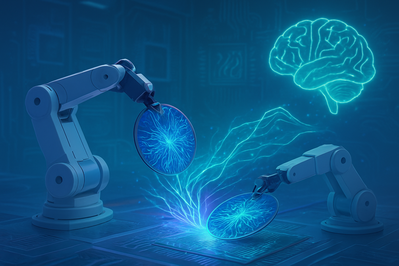
The core of QuantumDiamonds' innovation lies in its Quantum Diamond Microscopy (QDM) technology, which leverages nitrogen-vacancy (NV) centers embedded in synthetic diamonds. These atomic-scale defects act as highly sensitive quantum sensors, capable of detecting and measuring minute magnetic fields generated by electrical currents within a microchip. The QDM.1 system boasts impressive technical specifications, offering a lateral resolution down to 1 μm and a depth resolution down to 0.5 μm, capable of imaging metallization with feature sizes as small as 200 nm. Crucially, it provides 3D insight into chip defects with a depth reach of up to 500 µm and can image wide fields of view up to 3mm x 3mm, with automatic stitching for larger areas. Operating robustly at room temperature, QDM eliminates the need for complex cryogenic or vacuum setups, a significant advantage over some advanced testing methods. The system also integrates smart software and AI for rapid data analysis, converting magnetic field data into detailed, machine learning-enhanced 3D interactive visualizations of electrical activity.
This approach fundamentally differs from previous microchip testing methods, which often suffer from limitations in invasiveness, speed, and visibility. Conventional techniques like optical scanning, thermal imaging, lock-in thermography, and CT X-ray imaging struggle with the multi-layered complexity of modern chips. Optical microscopes, for instance, typically only view the first layer, rendering deeper defects invisible. QDM, by contrast, images magnetic fields that penetrate all layers, providing a comprehensive, non-destructive 3D view of internal flaws. It offers significantly higher resolution (up to 100 times smaller details), lower noise (100-1,000 times lower), and higher sensitivity (3-10 times) compared to traditional tools, enabling faster and more accurate fault localization.
Initial reactions from the AI research community and industry experts have been overwhelmingly positive. QuantumDiamonds has already partnered with nine of the ten largest chip manufacturers globally for proof-of-concept projects, demonstrating strong industry validation. Dr. David Su, former director of TSMC's (TWSE: 2330) (NYSE: TSM) failure analysis team and now a QuantumDiamonds advisor, has highlighted the technology's "significant promise" in addressing non-destructive fault isolation in advanced packaging. The European Innovation Council has even drawn comparisons between QuantumDiamonds' potential and that of ASML (AMS: ASML) (NASDAQ: ASML), a global leader in semiconductor lithography, underscoring its perceived revolutionary impact on post-production enablement. The sentiment is that QDM is a "game-changer" for the semiconductor industry, crucial for the continued advancement of Moore's Law and the escalating demands of the AI era.
Industry Repercussions: How QuantumDiamonds Shapes AI and Tech Giants
QuantumDiamonds' new Munich plant and its QDM technology are set to profoundly reshape the competitive landscape for AI companies, tech giants, and startups. Companies developing AI hardware and software stand to gain immensely from the promise of higher quality, more reliable, and ultimately more affordable high-performance chips. As AI workloads push chipmakers towards denser, more complex architectures, the ability to accurately detect and localize defects within these intricate designs becomes paramount for optimal AI performance and reduced failure rates. This technology also offers enhanced cybersecurity by detecting malicious alterations in chips, thereby strengthening the reliability of critical AI systems.
Major tech giants, often at the forefront of chip design and manufacturing, will benefit significantly from improved production yields and accelerated innovation cycles. The QDM technology enables them to detect previously invisible defects, leading to better chip designs, enhanced production efficiency, and substantial cost reductions in their semiconductor manufacturing processes. Companies like TSMC (TWSE: 2330) (NYSE: TSM) and Intel (NASDAQ: INTC), which has already inspected microchips using QuantumDiamonds' sensors, are actively engaging with this technology. For startups in AI hardware or specialized chip development, access to more precise and non-destructive testing can accelerate their development timelines, reduce prototyping costs, and improve the market readiness of their innovative chip designs, potentially leveling the playing field.
The competitive implications are clear: major AI labs and tech companies that integrate QDM into their R&D and production processes will gain a significant edge, producing more reliable and higher-performing chips, leading to faster time-to-market and substantial cost efficiencies. This disruptive technology is poised to render many conventional inspection methods obsolete. QDM's ability to provide non-destructive, 3D, layer-specific insights into complex chip packages—avoiding damage and allowing tested chips to be sold—is a game-changer. QuantumDiamonds has strategically positioned itself as a pioneer, backed by strong industry validation, significant public investment under the European Chips Act, and a global demand for its unique capabilities, with the European Innovation Council likening its potential to that of ASML.
Broader Horizons: Quantum Sensing's Role in the Global Tech Landscape
QuantumDiamonds' Munich plant and QDM technology fit squarely into the broader AI landscape and current technological trends, particularly the escalating demand for advanced semiconductors to power AI, IoT, and high-performance computing. The ability to precisely test and validate these increasingly complex chips is crucial for the continued progress of AI, as defects can severely impede performance and inflate costs. This development also highlights the synergistic relationship between quantum technology and AI, where quantum sensing provides unprecedented data for AI-driven optimization processes in chip design and manufacturing.
The impact on the semiconductor industry is transformative. By providing superior defect detection capabilities, QDM addresses a critical bottleneck that traditional methods cannot resolve, leading to improved production efficiency, accelerated design cycles, higher yields, and lower costs. This translates to more reliable and affordable technology across all sectors reliant on advanced electronics. Beyond semiconductors, the underlying quantum sensing technology holds immense potential for applications in medical diagnostics, defense, energy, and materials science, suggesting a wider revolution in precision measurement.
While the promise is vast, challenges remain. Scaling production of quantum-grade diamond sensors, ensuring precise control of defect placement, and mitigating environmental noise are ongoing hurdles. The interpretation of "massive amounts of data" generated by QDM devices also requires sophisticated machine learning algorithms, which QuantumDiamonds has developed. The establishment of the Munich plant, however, is a direct and significant outcome of the European Chips Act, which aims to double Europe's global semiconductor production share to 20% by 2030. By choosing Germany for this facility, QuantumDiamonds reinforces Europe's position not just in manufacturing, but in high-value equipment and advanced metrology, making it a strategic player in the global semiconductor competition. This initiative is a critical step for Europe in securing its high-tech future and maintaining a competitive edge in an era of intense global competition for semiconductor dominance.
The Road Ahead: Future Trajectories for QuantumDiamonds and Quantum Sensing
QuantumDiamonds is embarking on an ambitious journey to scale its production and global footprint. In the near term, construction of the Munich facility is slated to begin immediately, signifying a crucial transition from research to global industrial production. This hub will encompass production lines for quantum-grade diamond substrates, cleanroom integration of QDM inspection systems, and joint development laboratories with semiconductor partners. Initial QDM system deployments have already commenced in Europe, with further installations planned for the first quarter of 2026 in the United States and Taiwan, targeting major semiconductor manufacturers.
Looking further ahead, QuantumDiamonds aims to become a foundational player in the semiconductor industry, with its long-term vision extending to developing next-generation metrology platforms that continually push the boundaries of chipmaking. The company plans to expand its QDM technology beyond magnetic field sensing to incorporate temperature sensing using NV centers in diamonds. Beyond semiconductors, the broader field of quantum sensing, including diamond-based technologies, holds immense potential for diverse sectors such as medical diagnostics, defense, energy exploration, civil engineering, and materials science. Experts predict quantum sensing will revolutionize conventional semiconductor testing, enabling unprecedented fault localization and significantly improving efficiency and yields.
However, challenges for broader adoption include standardization and industrialization of quantum sensor manufacturing, miniaturization and cost reduction for mass-market applications, and the development of a robust quantum sensing ecosystem. The talent shortage in highly specialized fields like quantum technology also remains a concern. Despite these hurdles, experts widely regard quantum sensing as the most mature segment of quantum technology, with a clear path to industrial scaling and significant market growth projected, particularly in the semiconductor sector.
Conclusion: A New Era for Semiconductor Quality and AI Innovation
QuantumDiamonds' investment in a state-of-the-art microchip testing plant in Munich represents a monumental stride forward for the semiconductor industry and the future of AI. By commercializing Quantum Diamond Microscopy, the company is introducing a disruptive technology that addresses critical inspection bottlenecks in advanced chip manufacturing, promising unprecedented levels of quality, performance, and efficiency. This development not only bolsters Europe's strategic position in the global semiconductor landscape under the European Chips Act but also lays the groundwork for more reliable, powerful, and secure AI-driven technologies.
The key takeaways are clear: QDM offers non-destructive, ultra-precise 3D defect detection that surpasses conventional methods, significantly improving chip yields and reducing costs. This innovation is crucial for the continued advancement of AI and high-performance computing, where complex chip architectures demand flawless components. In the coming weeks and months, observers should closely watch the commencement of construction for the Munich facility, the planned international deployments of QDM systems, and further developments in QuantumDiamonds' product roadmap, particularly their ambition to launch in-line quality control products for fabrication lines around 2028. The expansion of quantum sensing capabilities beyond magnetic fields will also be a key indicator of its long-term impact across diverse industries. QuantumDiamonds is not just building a plant; it is forging a new era for semiconductor quality and AI innovation.
This content is intended for informational purposes only and represents analysis of current AI developments.
TokenRing AI delivers enterprise-grade solutions for multi-agent AI workflow orchestration, AI-powered development tools, and seamless remote collaboration platforms.
For more information, visit https://www.tokenring.ai/.